
Æ
DAC853
4
www.ti.com
Resistor
Network
8
18
Data
Buffer A
DAC
Register A
Data
Buffer D
DAC
Register D
DAC A
DAC D
Buffer
Control
Register
Control
Power-Down
Control Logic
V
OUT
A
V
OUT
B
V
OUT
C
V
OUT
D
V
REF
L
A0
A1
A2
A3
GND
I
2
C Block
SCL
SDA
LDAC
V
REF
H
IOV
DD
V
DD
DAC8574
SLAS377A ≠ JANUARY 2003 ≠ REVISED JUNE 2003
QUAD, 16-BIT, LOW-POWER, VOLTAGE OUTPUT,
I
2
C INTERFACE DIGITAL-TO-ANALOG CONVERTER
FEATURES
DESCRIPTION
∑
Micropower Operation: 950 µA at 5 V V
DD
The DAC8574 is a low-power, quad channel, 16-bit
∑
Power-On Reset to Zero
buffered voltage output DAC. Its on-chip precision out-
put amplifier allows rail-to-rail output swing to be
∑
+2.7 V to +5.5 V Analog Power Supply
achieved. The DAC8574 utilizes an I
2
C compatible two
∑
16-Bit Monotonic
wire serial interface supporting high-speed interface
∑
Settling Time: 10µs to
±0.003% FSR
mode with address support of up to sixteen DAC8574's
∑
I
2
CTM Interface Up to 3.4 Mbps
for a total of 64 channels on the bus.
∑
Data Transmit Capability
The DAC8574 requires an external reference voltage
∑
On-Chip Output Buffer Amplifier, Rail-to-Rail
to set the output range of the DAC. The DAC8574
Operation
incorporates a power-on-reset circuit that ensures that
the DAC output powers up at zero volts and remains
∑
Double-Buffered Input Register
there until a valid write takes place to the device. The
∑
Address Support for up to Sixteen DAC8574s
DAC8574 contains a power-down feature, accessed
∑
Synchronous Update Support for up to 64
via the internal control register, that reduces the current
Channels
consumption of the device to 200 nA at 5 V.
∑
Operation From -40
∞C to 105∞C
The low power consumption of this part in normal
∑
Small 16 Lead TSSOP Package
operation makes it ideally suited to portable battery
operated equipment. The power consumption is less
APPLICATIONS
than 5 mW at V
DD
= 5 V reducing to 1 µW in
power-down mode.
∑
Process Control
The DAC8574 is available in a 16-lead TSSOP pack-
∑
Data Acquisition Systems
age.
∑
Closed-Loop Servo Control
∑
PC Peripherals
∑
Portable Instrumentation
I2C is a trademark of Philips Corporation.
Please be aware that an important notice concerning availability, standard warranty, and use in critical applications of Texas Instruments
semiconductor products and disclaimers thereto appears at the end of this data sheet.
PRODUCTION DATA information is current as of publication date.
Copyright © 2003, Texas Instruments Incorporated
Products conform to specifications per the terms of Texas Instruments
standard warranty. Production processing does not necessarily in-
clude testing of all parameters.
www.ti.com
3
A3
A2
A1
1
2
3
4
5
6
7
8
16
15
14
1
12
11
10
9
V
OUT
A
V
OUT
B
V
REF
H
V
DD
V
REF
L
GND
V
OUT
C
V
OUT
D
A0
IOV
DD
SDA
SCL
LDAC
DAC8574
DAC8574
SLAS377A ≠ JANUARY 2003 ≠ REVISED JUNE 2003
This integrated circuit can be damaged by ESD. Texas Instruments recommends that all integrated
circuits be handled with appropriate precautions. Failure to observe proper handling and installation
procedures can cause damage.
ESD damage can range from subtle performance degradation to complete device failure. Precision
integrated circuits may be more susceptible to damage because very small parametric changes could
cause the device not to meet its published specifications.
PACKAGE/ORDERING INFORMATION
PRODUCT
PACKAGE
PACKAGE
SPECIFICATION
PACKAGE
ORDERING
TRANSPORT MEDIA
DRAWING
TEMPERATURE
MARKING
NUMBER
NUMBER
RANGE
DAC8574
16-TSSOP
PW
-40
∞C TO +105∞C
D8574I
DAC8574IPW
90 Piece Tube
DAC8574IPWR
2000 Piece Tape and Reel
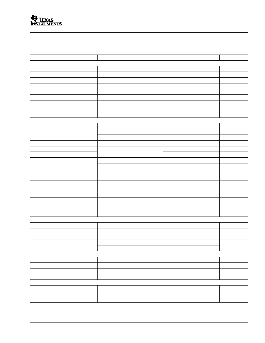
PW PACKAGE
PIN DESCRIPTIONS
(TOPVIEW)
PIN
NAME
DESCRIPTION
1
V
OUT
A
Analog output voltage from DAC A
2
V
OUT
B
Analog output voltage from DAC B
3
V
REF
H
Positive reference voltage input
4
V
DD
Analog voltage supply input
5
V
REF
L
Negative reference voltage input
Ground reference point for all circuitry on the
6
GND
part
7
V
OUT
C
Analog output voltage from DAC C
8
V
OUT
D
Analog output voltage from DAC D
9
LDAC
H/W synchronous V
OUT
update
10
SCL
Serial clock input
11
SDA
Serial data input
12
IOV
DD
I/O voltage supply input
13
A0
Device address select - I
2
C
14
A1
Device address select - I
2
C
15
A2
Device address select - Extended
16
A3
Device address select - Extended
ABSOLUTE MAXIMUM RATINGS (1)
V
DD
to GND
-0.3 V to +6 V
Digital input voltage to GND
-0.3 V to V
DD
+ 0.3 V
V
OUT
to GND
0.3 V to V
DD
+ 0.3 V
Operating temperature range
40
∞C to +105∞C
Storage temperature range
65
∞C to +150∞C
Junction temperature range (T
J
max)
+150
∞C
Power dissipation:
Thermal impedance (
JA)
118
∞C/W
Thermal impedance (
JC)
29
∞C/W
Lead temperature, soldering:
Vapor phase (60s)
215
∞C
Infrared (15s)
220
∞C
(1)
Stresses above those listed under Absolute Maximum Ratings may cause permanent damage to the device. Exposure to absolute
maximum conditions for extended periods may affect device reliability.
2
www.ti.com
DAC8574
SLAS377A ≠ JANUARY 2003 ≠ REVISED JUNE 2003
ELECTRICAL CHARACTERISTICS
V
DD
= 2.7 V to 5.5 V, R
L
= 2 k
to GND; C
L
= 200 pF to GND; all specifications -40
∞C to +105∞C, unless otherwise specified.
PARAMETER
TEST CONDITIONS
MIN
TYP
MAX
UNITS
STATIC PERFORMANCE (1) (2)
Resolution
16
Bits
Relative accuracy
± 0.0987
% of FSR
Differential nonlinearity
Specified monotonic by design
± 1
LSB
Zero-scale error
5
20
mV
Full-scale error
-0.15
±1.0
% of FSR
Gain error
± 1.0
% of FSR
Zero code error drift
±7
µV/
∞C
Gain temperature coefficient
± 3
ppm of FSR/
∞C
PSRR
V
DD
= 5 V
0.75
mV/V
OUTPUT CHARACTERISTICS (3)
Output voltage range
0
V
REF
H
V
Output voltage settling time (full scale)
R
L
= 2 k
; 0 pF < C
L
< 200 pF
8
10
µs
R
L
= 2 k
; C
L
= 500 pF
12
µs
Slew rate
1
V/µs
DC crosstalk
0.25
LSB
AC crosstalk
1 kHz Sine Wave
-100
-96
dB
Capacitive load stability
R
L
=
470
pF
R
L
= 2 k
1000
pF
Digital-to-analog glitch impulse
1 LSB change around major carry
20
nV-s
Digital feedthrough
0.5
nV-s
DC output impedance
1
Short-circuit current
V
DD
= 5 V
50
mA
V
DD
= 3 V
20
mA
Power-up time
Coming out of power-down mode, V
DD
=
2.5
µs
+5 V
Coming out of power-down mode, V
DD
=
5
µs
+3 V
REFERENCE INPUT
V
REF
H Input range
0
V
DD
V
V
REF
L Input range
V
REF
L < V
REF
H
0
GND
V
DD
V
Reference input impedance
35
k
Reference current
V
REF
=V
DD
= +5 V
135
180
µA
V
REF
=V
DD
= +3 V
80
120
LOGIC INPUTS (3)
Input current
± 1
µA
V
IN_L
, Input low voltage
0.3xIOV
DD
V
V
IN_H
, Input high voltage
V
DD
= 3 V
0.7xIOV
DD
V
Pin Capacitance
3
pF
POWER REQUIREMENTS
V
DD
, IOV
DD
2.7
5.5
V
I
DD
(normal operation)
Excluding load current
I
DD
@ V
DD
=+3.6V to +5.5V
V
IH
= IOV
DD
and V
IL
=GND
950
1600
µA
(1)
Linearity tested using a reduced code range of 485 to 64714; output unloaded.
(2)
V
REF
H = V
DD
- 0.1 V, V
REF
L = GND
(3)
Specified by design and characterization, not production tested.
3
www.ti.com
DAC8574
SLAS377A ≠ JANUARY 2003 ≠ REVISED JUNE 2003
ELECTRICAL CHARACTERISTICS (continued)
V
DD
= 2.7 V to 5.5 V, R
L
= 2 k
to GND; C
L
= 200 pF to GND; all specifications -40
∞C to +105∞C, unless otherwise specified.
PARAMETER
TEST CONDITIONS
MIN
TYP
MAX
UNITS
I
DD
@ V
DD
=+2.7V to +3.6V
V
IH
= IOV
DD
and V
IL
=GND
900
1500
µA
I
DD
(all power-down modes)
I
DD
@ V
DD
=+3.6V to +5.5V
V
IH
= IOV
DD
and IOV
IL
=GND
0.2
1
µA
I
DD
@ V
DD
=+2.7V to +3.6V
V
IH
= V
DD
and V
IL
=GND
0.05
1
µA
POWER EFFICIENCY
I
OUT
/I
DD
I
LOAD
= 2 mA, V
DD
= +5 V
93%
TEMPERATURE RANGE
Specified performance
-40
+105
∞C
TIMING CHARACTERISTICS
V
DD
= 2.7 V to 5.5 V, R
L
= 2 k
to GND; all specifications -40∞C to +105∞C, unless otherwise specified.
SYMBOL
PARAMETER
TEST CONDITIONS
MIN
TYP
MAX
UNITS
Standard mode
100
kHz
Fast mode
400
kHz
f
SCL
SCL clock frequency
High-Speed Mode, C
B
= 100 pF
3.4
MHz
max
High-speed mode, C
B
= 400 pF max
1.7
MHz
Standard mode
4.7
µs
Bus free time between a
t
BUF
STOP and START condition
Fast mode
1.3
µs
Standard mode
4.0
µs
Hold time (repeated) START
t
HD
; t
STA
Fast mode
600
ns
condition
High-speed mode
160
ns
Standard mode
4.7
µs
Fast mode
1.3
µs
t
LOW
LOW period of the SCL clock
High-speed mode, C
B
= 100 pF max
160
ns
High-speed mode, C
B
= 400 pF max
320
ns
Standard mode
4.0
µs
Fast mode
600
ns
t
HIGH
HIGH period of the SCL clock
High-Speed Mode, C
B
= 100 pF
60
ns
max
High-speed mode, C
B
= 400 pF max
120
ns
Standard mode
4.7
µs
Setup time for a repeated
t
SU
; t
STA
Fast mode
600
ns
START condition
High-speed mode
160
ns
Standard mode
250
ns
t
SU
; t
DAT
Data setup time
Fast mode
100
ns
High-speed mode
10
ns
Standard mode
0
3.45
µs
Fast mode
0
0.9
µs
t
HD
; t
DAT
Data hold time
High-speed mode, C
B
= 100 pF max
0
70
ns
High-speed mode, C
B
= 400 pF max
0
150
ns
Standard mode
20
◊ 0.1C
B
1000
ns
Fast mode
20
◊ 0.1C
B
300
ns
t
RCL
Rise time of SCL signal
High-speed mode, C
B
= 100 pF max
10
40
ns
High-speed mode, C
B
= 400 pF max
20
80
ns
4
www.ti.com
DAC8574
SLAS377A ≠ JANUARY 2003 ≠ REVISED JUNE 2003
TIMING CHARACTERISTICS (continued)
V
DD
= 2.7 V to 5.5 V, R
L
= 2 k
to GND; all specifications -40∞C to +105∞C, unless otherwise specified.
SYMBOL
PARAMETER
TEST CONDITIONS
MIN
TYP
MAX
UNITS
Standard mode
20
◊ 0.1C
B
1000
ns
Rise time of SCL signal after a
Fast mode
20
◊ 0.1C
B
300
ns
t
RCL1
repeated START condition
High-speed mode, C
B
= 100 pF max
10
80
ns
and after an acknowledge BIT
High-speed mode, C
B
= 400 pF max
20
160
ns
Standard mode
20
◊ 0.1C
B
300
ns
Fast mode
20
◊ 0.1C
B
300
ns
t
FCL
Fall time of SCL signal
High-speed mode, C
B
= 100 pF max
10
40
ns
High-speed mode, C
B
= 400 pF max
20
80
ns
Standard mode
20
◊ 0.1C
B
1000
ns
Fast mode
20
◊ 0.1C
B
300
ns
t
RDA
Rise time of SDA signal
High-speed mode, C
B
= 100 pF max
10
80
ns
High-speed mode, C
B
= 400 pF max
20
160
ns
Standard mode
20
◊ 0.1C
B
300
ns
Fast mode
20
◊ 0.1C
B
300
ns
t
FDA
Fall time of SDA signal
High-speed mode, C
B
= 100 pF max
10
80
ns
High-speed mode, C
B
= 400 pF max
20
160
ns
Standard mode
4.0
µs
t
SU
; t
STO
Setup time for STOP condition
Fast mode
600
ns
High-speed mode
160
ns
Capacitive load for SDA and
C
B
400
pF
SCL
Fast mode
50
ns
Pulse width of spike sup-
t
SP
pressed
High-speed mode
10
ns
Standard mode
Noise margin at the HIGH
V
NH
level for each connected de-
Fast mode
0.2 V
DD
V
vice (including hysteresis)
High-speed mode
Standard mode
Noise margin at the LOW level
V
NL
for each connected device
Fast mode
0.1 V
DD
V
(including hysteresis)
High-speed mode
5
www.ti.com
- 64
- 48
- 32
- 16
0
16
32
48
64
LE
-
LSB
Channel A
V
DD
= 5 V
- 1
- 0.5
0
0.5
1
Digital Input Code
DLE
-
LSB
0000
H
4000
H
6000
H
8000
H
A000 C000 E000 FFFF
H
H
H
H
2000
H
- 64
- 48
- 32
- 16
0
16
32
48
64
LE
-
LSB
Channel B
V
DD
= 5 V
- 1
- 0.5
0
0.5
1
Digital Input Code
DLE
-
LSB
0000
H
4000
H
6000
H
8000
H
A000 C000 E000 FFFF
H
H
H
H
2000
H
- 64
- 48
- 32
- 16
0
16
32
48
64
LE
-
LSB
Channel C
V
DD
= 5 V
- 1
- 0.5
0
0.5
1
Digital Input Code
DLE
-
LSB
0000
H
4000
H
6000
H
8000
H
A000 C000 E000 FFFF
H
H
H
H
2000
H
- 64
- 48
- 32
- 16
0
16
32
48
64
LE
-
LSB
Channel D
V
DD
= 5 V
- 1
- 0.5
0
0.5
1
Digital Input Code
DLE
-
LSB
0000
H
4000
H
6000
H
8000
H
A000 C000 E000 FFFF
H
H
H
H
2000
H
- 64
- 48
- 32
- 16
0
16
32
48
64
LE
-
LSB
Channel A
V
DD
= 2.7 V
- 1
- 0.5
0
0.5
1
Digital Input Code
DLE
-
LSB
0000
H
4000
H
6000
H
8000
H
A000 C000 E000 FFFF
H
H
H
H
2000
H
- 64
- 48
- 32
- 16
0
16
32
48
64
LE
-
LSB
Channel B
V
DD
= 2.7 V
- 1
- 0.5
0
0.5
1
Digital Input Code
DLE
-
LSB
0000
H
4000
H
6000
H
8000
H
A000 C000 E000 FFFF
H
H
H
H
2000
H
DAC8574
SLAS377A ≠ JANUARY 2003 ≠ REVISED JUNE 2003
TYPICAL CHARACTERISTICS
At T
A
= +25
∞C, unless otherwise noted.
LINEARITY ERROR AND DIFFERENTIAL
LINEARITY ERROR AND DIFFERENTIAL
LINEARITY ERROR vs DIGITAL INPUT CODE
LINEARITY ERROR vs DIGITAL INPUT CODE
Figure 1.
Figure 2.
LINEARITY ERROR AND DIFFERENTIAL
LINEARITY ERROR AND DIFFERENTIAL
LINEARITY ERROR vs DIGITAL INPUT CODE
LINEARITY ERROR vs DIGITAL INPUT CODE
Figure 3.
Figure 4.
LINEARITY ERROR AND DIFFERENTIAL
LINEARITY ERROR AND DIFFERENTIAL
LINEARITY ERROR vs DIGITAL INPUT CODE
LINEARITY ERROR vs DIGITAL INPUT CODE
Figure 5.
Figure 6.
6

www.ti.com
- 64
- 48
- 32
- 16
0
16
32
48
64
LE
-
LSB
Channel C
V
DD
= 2.7 V
- 1
- 0.5
0
0.5
1
Digital Input Code
DLE
-
LSB
0000
H
4000
H
6000
H
8000
H
A000 C000 E000 FFFF
H
H
H
H
2000
H
- 64
- 48
- 32
- 16
0
16
32
48
64
LE
-
LSB
Channel D
V
DD
= 2.7 V
- 1
- 0.5
0
0.5
1
Digital Input Code
DLE
-
LSB
0000
H
4000
H
6000
H
8000
H
A000 C000 E000 FFFF
H
H
H
H
2000
H
- 2
0
2
4
6
8
10
- 40
- 10
20
50
80
110
Zero
-
Scale Error
-
mV
V
DD
= V
REF
= 2.7 V
CH A
CH D
CH B
CH C
T
A
- Free-Air Temperature -
∞
C
0
2
4
6
8
10
12
14
- 40
- 10
20
50
80
110
Zero
-
Scale Error
-
mV
V
DD
= V
REF
= 5 V
CH A
CH D
CH B
CH C
T
A
- Free-Air Temperature -
∞
C
- 15
- 10
- 5
0
5
10
15
- 40
- 10
20
50
80
110
F
ull
-
Scale Error
-
mV
CH A
CH D
CH B
CH C
To avoid clipping of the output signal
during the test, V
REF
= V
DD
- 10 mV,
V
DD
= 2.7 V, V
REF
= 2.69 V
T
A
- Free-Air Temperature -
∞
C
- 15
- 10
- 5
0
5
10
15
- 40
- 10
20
50
80
110
F
ull
-
Scale Error
-
mV
CH A
CH D
CH B
CH C
To avoid clipping of the output signal
during the test, V
REF
= V
DD
- 10 mV,
V
DD
= 5 V, V
REF
= 4.99 V
T
A
- Free-Air Temperature -
∞
C
DAC8574
SLAS377A ≠ JANUARY 2003 ≠ REVISED JUNE 2003
TYPICAL CHARACTERISTICS (continued)
At T
A
= +25
∞C, unless otherwise noted.
LINEARITY ERROR AND DIFFERENTIAL
LINEARITY ERROR AND DIFFERENTIAL
LINEARITY ERROR vs DIGITAL INPUT CODE
LINEARITY ERROR vs DIGITAL INPUT CODE
Figure 7.
Figure 8.
ZERO-SCALE ERROR
ZERO-SCALE ERROR
vs TEMPERATURE
vs TEMPERATURE
Figure 9.
Figure 10.
FULL-SCALE ERROR
FULL-SCALE ERROR
vs TEMPERATURE
vs TEMPERATURE
Figure 11.
Figure 12.
7
www.ti.com
0
0.025
0.05
0.075
0.1
0.125
0.15
0
1
2
3
4
5
I
SINK
- Sink Current - mA
V
OUT
-
Output
V
oltage
-
V
V
REF
= V
DD
- 10 mV
DAC Loaded With 0000
H
V
DD
= 2.7 V
V
DD
= 5 V
Channel A
0
0.025
0.05
0.075
0.1
0.125
0.15
0
1
2
3
4
5
I
SINK
- Sink Current - mA
V
OUT
-
Output
V
oltage
-
V
V
REF
= V
DD
- 10 mV
DAC Loaded With 0000
H
V
DD
= 2.7 V
V
DD
= 5 V
Channel B
0
0.025
0.05
0.075
0.1
0.125
0.15
0
1
2
3
4
5
I
SINK
- Sink Current - mA
V
OUT
-
Output
V
oltage
-
V
V
REF
= V
DD
- 10 mV
DAC Loaded With 0000
H
V
DD
= 2.7 V
V
DD
= 5 V
Channel C
0
0.025
0.05
0.075
0.1
0.125
0.15
0
1
2
3
4
5
I
SINK
- Sink Current - mA
V
OUT
-
Output
V
oltage
-
V
V
REF
= V
DD
- 10 mV
DAC Loaded With 0000
H
V
DD
= 2.7 V
V
DD
= 5 V
Channel D
4.8
4.85
4.9
4.95
5
0
1
2
3
4
5
I
SOURCE
- Source Current - mA
V
OUT
-
Output
V
oltage
-
V
V
REF
= V
DD
- 10 mV
DAC Loaded With FFFF
H
V
DD
= 5 V
Channel A
4.8
4.85
4.9
4.95
5
0
1
2
3
4
5
I
SOURCE
- Source Current - mA
V
OUT
-
Output
V
oltage
-
V
V
REF
= V
DD
- 10 mV
DAC Loaded With FFFF
H
V
DD
= 5 V
Channel B
DAC8574
SLAS377A ≠ JANUARY 2003 ≠ REVISED JUNE 2003
TYPICAL CHARACTERISTICS (continued)
At T
A
= +25
∞C, unless otherwise noted.
PULLDOWN CAPABILITY
PULLDOWN CAPABILITY
vs SINK CURRENT
vs SINK CURRENT
Figure 13.
Figure 14.
PULLDOWN CAPABILITY
PULLDOWN CAPABILITY
vs SINK CURRENT
vs SINK CURRENT
Figure 15.
Figure 16.
PULLUP CAPABILITY
PULLUP CAPABILITY
vs SOURCE CURRENT
vs SOURCE CURRENT
Figure 17.
Figure 18.
8

www.ti.com
4.8
4.85
4.9
4.95
5
0
1
2
3
4
5
I
SOURCE
- Source Current - mA
V
OUT
-
Output
V
oltage
-
V
V
REF
= V
DD
- 10 mV
DAC Loaded With FFFF
H
V
DD
= 5 V
Channel C
4.8
4.85
4.9
4.95
5
0
1
2
3
4
5
I
SOURCE
- Source Current - mA
V
OUT
-
Output
V
oltage
-
V
V
REF
= V
DD
- 10 mV
DAC Loaded With FFFF
H
V
DD
= 5 V
Channel D
2.5
2.55
2.6
2.65
2.7
0
1
2
3
4
5
I
SOURCE
- Source Current - mA
V
OUT
-
Output
V
oltage
-
V
V
REF
= V
DD
- 10 mV
DAC Loaded With FFFF
H
V
DD
= 2.7 V
Channel A
2.5
2.55
2.6
2.65
2.7
0
1
2
3
4
5
I
SOURCE
- Source Current - mA
V
OUT
-
Output
V
oltage
-
V
V
REF
= V
DD
- 10 mV
DAC Loaded With FFFF
H
V
DD
= 2.7 V
Channel B
2.5
2.55
2.6
2.65
2.7
0
1
2
3
4
5
I
SOURCE
- Source Current - mA
V
OUT
-
Output
V
oltage
-
V
V
REF
= V
DD
- 10 mV
DAC Loaded With FFFF
H
V
DD
= 2.7 V
Channel C
2.5
2.55
2.6
2.65
2.7
0
1
2
3
4
5
I
SOURCE
- Source Current - mA
V
OUT
-
Output
V
oltage
-
V
V
REF
= V
DD
- 10 mV
DAC Loaded With FFFF
H
V
DD
= 2.7 V
Channel D
DAC8574
SLAS377A ≠ JANUARY 2003 ≠ REVISED JUNE 2003
TYPICAL CHARACTERISTICS (continued)
At T
A
= +25
∞C, unless otherwise noted.
PULLUP CAPABILITY
PULLUP CAPABILITY
vs SOURCE CURRENT
vs SOURCE CURRENT
Figure 19.
Figure 20.
PULLUP CAPABILITY
PULLUP CAPABILITY
vs SOURCE CURRENT
vs SOURCE CURRENT
Figure 21.
Figure 22.
PULLUP CAPABILITY
PULLUP CAPABILITY
vs SOURCE CURRENT
vs SOURCE CURRENT
Figure 23.
Figure 24.
9
www.ti.com
V
DD
= V
REF
= 5 V
1200
1000
800
600
400
200
0
I
DD
µ
A
0000
H
2000
H
4000
H
6000
H
8000
H
Digital Input Code
A000
H
C000
H
E000
H
FFFF
H
V
DD
= V
REF
= 2.7 V
-
S
u
p
p
l
y
C
u
r
r
e
n
t
-
V
DD
= V
REF
= 5 V
V
DD
= V
REF
= 2.7 V
Reference Current Included
1200
1000
800
600
400
200
0
I
DD
µ
A
-
Supply Current
-
T
A
- Free - Air Temperature -
o
C
All Channels Powered, No Load
- 40
- 10
20
50
80
110
1000
950
900
850
800
750
700
650
600
2.7
3.05
3.4
3.75
4.1
4.45
4.8
5.15
5.5
V
DD
- Supply Voltage - V
I
DD
µ
A
-
Supply Current
-
V
DD
= V
REF
= 2.7 V
1750
1650
1550
1450
1350
1250
1150
1050
950
850
750
0
0.5
1.0
1.5
2.0
2.5
3.0
3.5
4.0
4.5
5.0
T
A
= 25
_
C, A0 Input (All Other Inputs = GND)
Reference Current Included
I
DD
+ IOI
-
Supply Current
-
DD
µ
A
IOV
DD
= 5 V
V
LOGIC
- Logic Input Voltage - V
V
DD
= V
REF
= 5 V
Reference Current Included
1500
1000
500
0
F
requency
820
790
850
880
910
940
970
1000
1030
1060
1090
1
120
1
150
I
DD
µ
A
- Current Consumption -
V
DD
= V
REF
= 2.7 V
Reference Current Included
1500
1000
500
0
F
requency
820
790
760
730
850
880
910
940
970
1000
1030
1060
I
DD
µ
A
- Current Consumption -
DAC8574
SLAS377A ≠ JANUARY 2003 ≠ REVISED JUNE 2003
TYPICAL CHARACTERISTICS (continued)
At T
A
= +25
∞C, unless otherwise noted.
SUPPLY CURRENT
SUPPLY CURRENT
vs DIGITAL INPUT CODE
vs TEMPERATURE
Figure 25.
Figure 26.
SUPPLY CURRENT
SUPPLY CURRENT
vs SUPPLY VOLTAGE
vs LOGIC INPUT VOLTAGE
Figure 27.
Figure 28.
HISTOGRAM OF CURRENT CONSUMPTION
HISTOGRAM OF CURRENT CONSUMPTION
Figure 29.
Figure 30.
10

www.ti.com
- 0.5
0.0
0.5
1.0
1.5
2.0
2.5
3.0
3.5
4.0
4.5
5.0
5.5
V
DD
= V
REF
= 5 V
Power- Up Code = FFFF
H
Time (4
µ
s/div)
V
O
U
T
-
Output V
oltage
-
V
2.43
2.44
2.45
2.46
2.47
2.48
2.49
2.50
2.51
2.52
2.53
V
DD
= V
REF
= 5 V
Code 7FFF
H
to 8000
H
to 7FFF
H
(Glitch Occurs Every N
∑
4096
Code Boundary)
Time (1
µ
s/div)
V
O
U
T
(V
, 10 mV/div)
4.54
4.56
4.58
4.60
4.62
4.64
4.66
4.68
4.70
4.72
V
DD
= V
REF
= 5 V
Code EFFF
H
to F000
H
to EFFF
H
(Glitch Occurs Every N
∑
4096
Code Boundary)
Time (1
µ
s/div)
V
O
U
T
(V
, 20 mV/div)
Digital Input Code
0
2
4
6
8
10
12
14
16
18
20
0000
H
2000
H
4000
H
6000
H
8000
H
A000
H
C000
H
E000
H
FFFF
H
Output Error
-
mV
V
DD
= V
REF
= 5 V
T
A
= 25
∞
C
Channel D Output
Channel B Output
Channel C Output
Channel A Output
0
1
2
3
4
5
6
V
DD
= V
REF
= 5.5 V
Output Loaded with
2 k
and 200 pF
to GND
Time (12
µ
s/div)
V
O
U
T
-
Output V
oltage
-
V
Digital Input Code
- 10
- 8
- 6
- 4
- 2
0
2
4
6
8
10
0000
H
2000
H
4000
H
6000
H
8000
H
A000
H
C000
H
E000
H
FFFF
H
Output Error
-
mV
Channel B Output
Channel D Output
Channel A Output
Channel C Output
V
DD
= V
REF
= 2.7 V
T
A
= 25
∞
C
DAC8574
SLAS377A ≠ JANUARY 2003 ≠ REVISED JUNE 2003
TYPICAL CHARACTERISTICS (continued)
At T
A
= +25
∞C, unless otherwise noted.
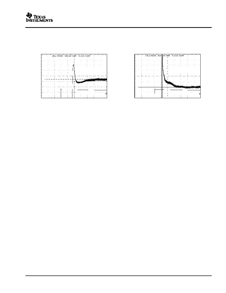
EXITING POWER-DOWN MODE
OUTPUT GLITCH (Mid-Scale)
Figure 31.
Figure 32.
OUTPUT GLITCH (Worst Case)
ABSOLUTE ERROR
Figure 33.
Figure 34.
FULL-SCALE SETTLING TIME
ABSOLUTE ERROR
(Large Signal)
Figure 35.
Figure 36.
11
www.ti.com
0.0
0.5
1.0
1.5
2.0
2.5
3.0
V
DD
= V
REF
= 5 V
Output Loaded with
2 k
and 200 pF
to GND
Time (12
µ
s/div)
V
O
U
T
-
Output V
oltage
-
V
0.0
0.5
1.0
1.5
2.0
2.5
3.0
3.5
V
DD
= V
REF
= 2.7 V
Output Loaded with
2 k
and 200 pF
to GND
Time (12
µ
s/div)
V
O
U
T
-
Output V
oltage
-
V
0.00
0.50
1.00
1.50
V
DD
= V
REF
= 2.7 V
Output Loaded with
2 k
and 200 pF to
GND
Time (12
µ
s/div)
V
O
U
T
-
Output V
oltage
-
V
V
DD
= 5 V
V
DD
= 2.7 V
V
DD
= V
REF
1 dB FSR Digital Input, F
-
S
= 52 ksps
Measurement Bandwidth = 20 kHz
98
96
94
92
90
88
86
84
SNR
-
Signal
-
to
-
Noise Ratio
-
dB
0
500
1k
1.5k
2k
2.5k
3k
3.5k
4k
4.5k
f - Output Frequency - Hz
V
DD
= V
REF
= 5 V
F
S
= 52 ksps, - 1 dB FSR Digital Input
Measurement Bandwidth = 20 kHz
THD
2nd Harmonic
3rd Harmonic
0
- 10
- 20
- 30
- 40
- 50
- 60
- 70
- 80
- 90
- 100
THD
-
T
otal Harmonic Distortion
-
dB
0
500
1k
1.5k
2k
2.5k
3k
3.5k
4k
f - Output Frequency - Hz
V
DD
= V
REF
= 2.7 V
F
S
= 52 ksps, - 1 dB FSR Digital Input
Measurement Bandwidth = 20 kHz
THD
2nd Harmonic
3rd Harmonic
0
- 10
- 20
- 30
- 40
- 50
- 60
- 70
- 80
- 90
-100
0
500
1k
1.5k
2k
2.5k
3k
3.5k
4k
THD
-
T
otal Harmonic Distortion
-
dB
f - Output Frequency - Hz
DAC8574
SLAS377A ≠ JANUARY 2003 ≠ REVISED JUNE 2003
TYPICAL CHARACTERISTICS (continued)
At T
A
= +25
∞C, unless otherwise noted.
HALF-SCALE SETTLING TIME
FULL-SCALE SETTLING TIME
(Large Signal)
(Large Signal)
Figure 37.
Figure 38.
SIGNAL-TO-NOISE RATIO
HALF-SCALE SETTLING TIME
vs OUTPUT FREQUENCY
Figure 39.
Figure 40.
TOTAL HARMONIC DISTORTION
TOTAL HARMONIC DISTORTION
vs OUTPUT FREQUENCY
vs OUTPUT FREQUENCY
Figure 41.
Figure 42.
12
www.ti.com
Small- Signal Settling Time
5mV/div
Time (2
µ
s/div)
Output V
oltage
Trigger Signal
Small- Signal Settling Time
5mV/div
Time (2
µ
s/div)
Output V
oltage
Trigger Signal
DAC8574
SLAS377A ≠ JANUARY 2003 ≠ REVISED JUNE 2003
TYPICAL CHARACTERISTICS (continued)
At T
A
= +25
∞C, unless otherwise noted.
FULL-SCALE SETTLING TIME
FULL-SCALE SETTLING TIME
(Small-Signal-Positive Going Step)
(Small-Signal-Negative Going Step)
Figure 43.
Figure 44.
13
www.ti.com
_
+
Resistor String
Ref+
Ref-
DAC Register
V
OUT
50 k
W
50 k
W
V
REF
H
V
REF
L
70 k
W
V
OUT
+
V
REF
L
)
(V
REF
H
*
V
REF
L)
D
65536
(1)
V
REF
H
To Output
Amplifier
R
R
R
R
V
REF
L
DAC8574
SLAS377A ≠ JANUARY 2003 ≠ REVISED JUNE 2003
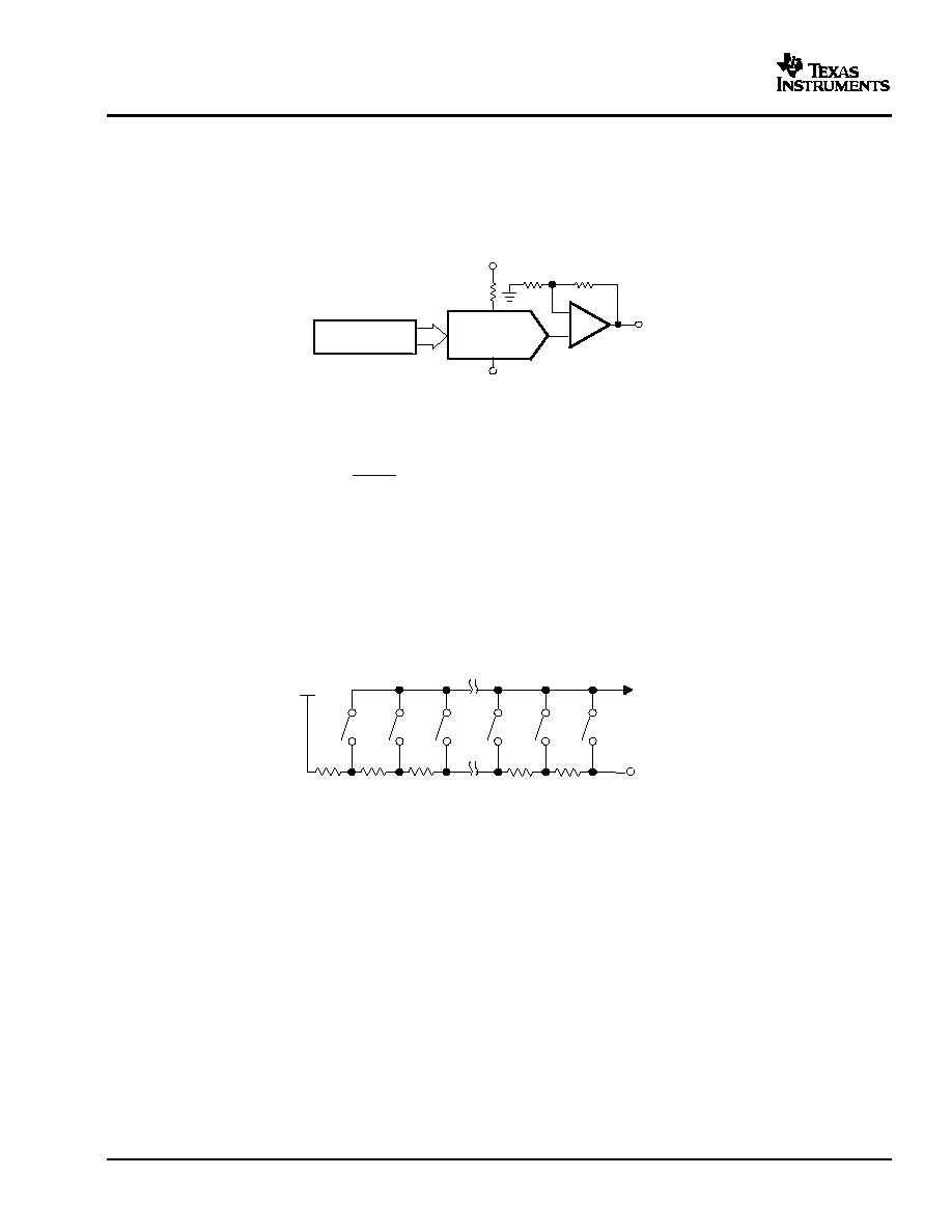
THEORY OF OPERATION
D/A SECTION
The architecture of the DAC8574 consists of a string DAC followed by an output buffer amplifier. Figure 45
shows a generalized block diagram of the DAC architecture.
Figure 45. R-String DAC Architecture
The input coding to the DAC8574 is unsigned binary, which gives the ideal output voltage as:
Where D = decimal equivalent of the binary code that is loaded to the DAC register; it can range from 0 to
65535.
RESISTOR STRING
The resistor string section is shown in Figure 46. It is basically a divide-by-2 resistor, followed by a string of
resistors, each of value R. The code loaded into the DAC register determines at which node on the string the
voltage is tapped off to be fed into the output amplifier by closing one of the switches connecting the string to the
amplifier. Because the architecture consists of a string of resistors, it is specified monotonic.
Figure 46. Typical Resistor String
Output Amplifier
The output buffer is a gain-of-2 noninverting amplifiers, capable of generating rail-to-rail voltages on its output,
which gives an output range of 0V to V
DD
. It is capable of driving a load of 2 k
in parallel with 1000 pF to GND.
The source and sink capabilities of the output amplifier can be seen in the typical curves. The slew rate is 1 V/µs
with a half-scale settling time of 8 µs with the output unloaded.
I
2
C Interface
I
2
C is a 2-wire serial interface developed by Philips Semiconductor (see I
2
C-Bus Specification, Version 2.1,
January 2000). The bus consists of a data line (SDA) and a clock line (SCL) with pullup structures. When the bus
is idle, both SDA and SCL lines are pulled high. All the I
2
C compatible devices connect to the I
2
C bus through
open drain I/O pins, SDA and SCL. A master device, usually a microcontroller or a digital signal processor,
controls the bus. The master is responsible for generating the SCL signal and device addresses. The master also
generates specific conditions that indicate the START and STOP of data transfer. A slave device receives and/or
transmits data on the bus under control of the master device.
14
www.ti.com
DAC8574
SLAS377A ≠ JANUARY 2003 ≠ REVISED JUNE 2003
THEORY OF OPERATION (continued)
The DAC8574 works as a slave and supports the following data transfer modes, as defined in the I
2
C-Bus
Specification: standard mode (100 kbps), fast mode (400 kbps), and high-speed mode (3.4 Mbps). The data
transfer protocol for standard and fast modes is exactly the same, therefore they are referred to as F/S-mode in
this document. The protocol for high-speed mode is different from the F/S-mode, and it is referred to as
HS-mode. The DAC8574 supports 7-bit addressing; 10-bit addressing, and general call address are not
supported.
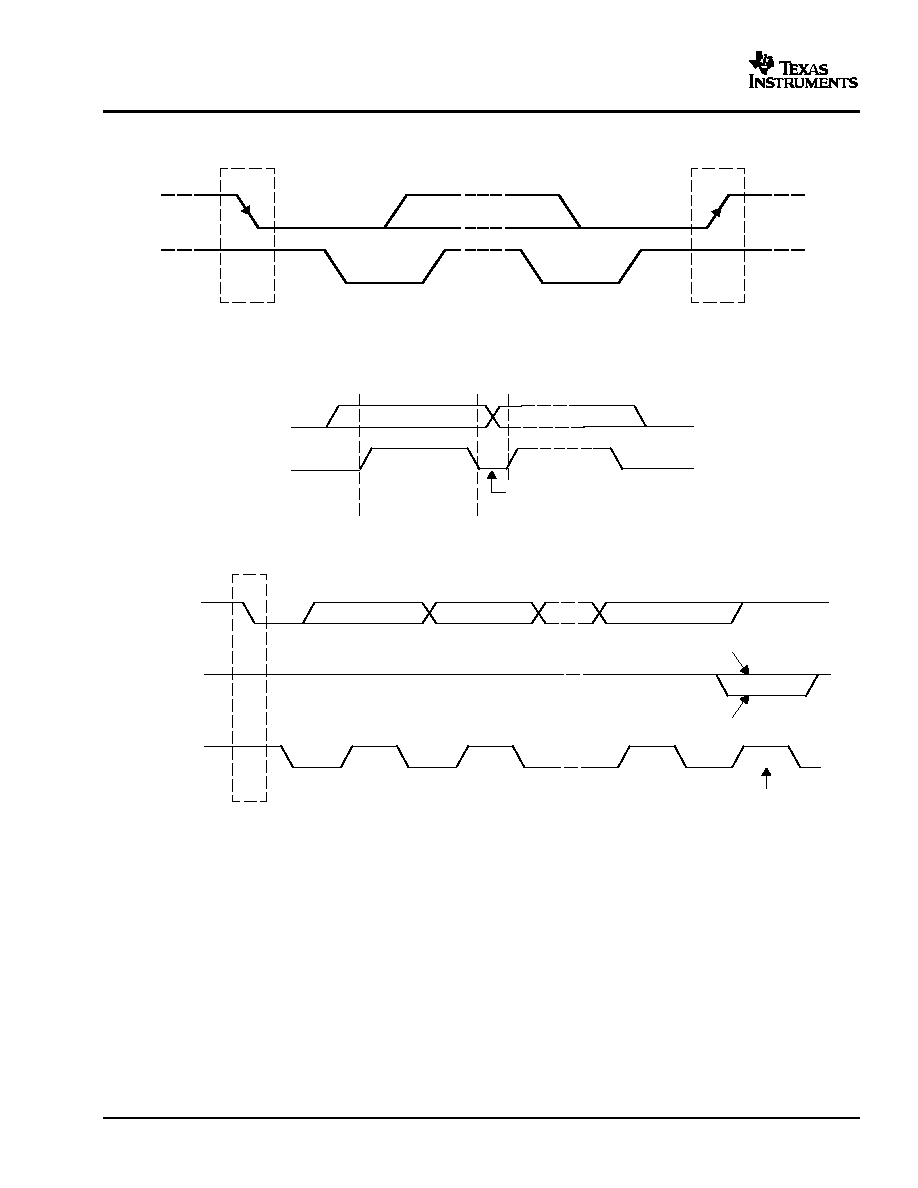
F/S-Mode Protocol
∑
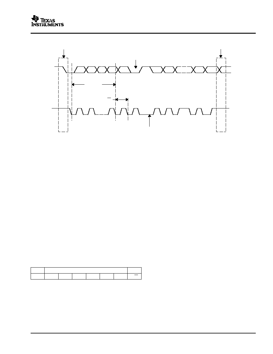
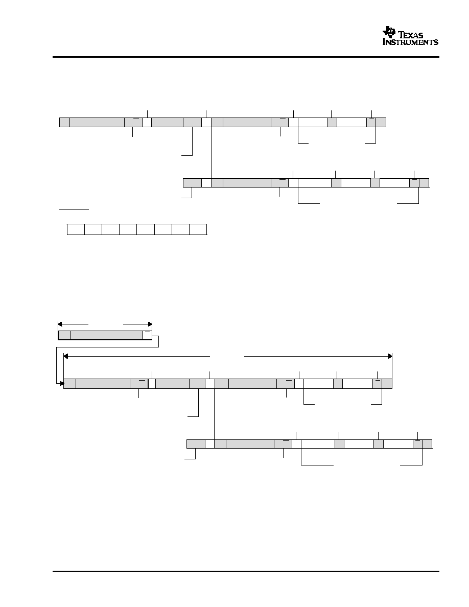
The master initiates data transfer by generating a start condition. The start condition is when a high-to-low
transition occurs on the SDA line while SCL is high, as shown in Figure 47. All I
2
C-compatible devices should
recognize a start condition.
∑
The master then generates the SCL pulses, and transmits the 7-bit address and the read/write direction bit
R/W on the SDA line. During all transmissions, the master ensures that data is valid. A valid data condition
requires the SDA line to be stable during the entire high period of the clock pulse (see Figure 48). All devices
recognize the address sent by the master and compare it to their internal fixed addresses. Only the slave
device with a matching address generates an acknowledge (see Figure 49) by pulling the SDA line low
during the entire high period of the 9th SCL cycle. Upon detecting this acknowledge, the master knows that
communication link with a slave has been established.
∑
The master generates further SCL cycles to either transmit data to the slave (R/W bit 1) or receive data from
the slave (R/W bit 0). In either case, the receiver needs to acknowledge the data sent by the transmitter. So
acknowledge signal can either be generated by the master or by the slave, depending on which one is the
receiver. 9-bit valid data sequences consisting of 8-bit data and 1-bit acknowledge can continue as long as
necessary.
∑
To signal the end of the data transfer, the master generates a stop condition by pulling the SDA line from low
to high while the SCL line is high (see Figure 47). This releases the bus and stops the communication link
with the addressed slave. All I
2
C compatible devices must recognize the stop condition. Upon the receipt of a
stop condition
, all devices know that the bus is released, and they wait for a start condition followed by a
matching address.
H/S-Mode Protocol
∑
When the bus is idle, both SDA and SCL lines are pulled high by the pullup devices.
∑
The master generates a start condition followed by a valid serial byte containing H/S master code
00001XXX. This transmission is made in F/S-mode at no more than 400 Kbps. No device is allowed to
acknowledge the H/S master code, but all devices must recognize it and switch their internal setting to
support 3.4 Mbps operation.
∑
The master then generates a repeated start condition (a repeated start condition has the same timing as the
start condition). After this repeated start condition, the protocol is the same as F/S-mode, except that
transmission speeds up to 3.4 Mbps are allowed. A stop condition ends the H/S-mode and switches all the
internal settings of the slave devices to support the F/S-mode. Instead of using a stop condition, repeated
start conditions should be used to secure the bus in H/S-mode.
15
www.ti.com
Start
Condition
SDA
Stop
Condition
SDA
SCL
S
P
SCL
Change of Data Allowed
Data Line
Stable;
Data Valid
SDA
SCL
Not Acknowledge
Acknowledge
1
2
8
9
Clock Pulse for
Acknowledgement
S
START
Condition
Data Output
by Transmitter
Data Output
by Receiver
SCL From
Master
DAC8574
SLAS377A ≠ JANUARY 2003 ≠ REVISED JUNE 2003
THEORY OF OPERATION (continued)
Figure 47. START and STOP Conditions
Figure 48. Bit Transfer on the I
2
C Bus
Figure 49. Acknowledge on the I
2
C Bus
16
www.ti.com
Recognize START or
REPEATED START
Condition
Recognize STOP or
REPEATED START
Condition
Generate ACKNOWLEDGE
Signal
Acknowledgement
Signal From Slave
SDA
SCL
MSB
P
Sr
Sr
or
P
S
or
Sr
START or
Repeated START
Condition
STOP or
Repeated START
Condition
Clock Line Held Low While
Interrupts are Serviced
1
2
7
8
9
ACK
1
2
3 - 8
9
ACK
Address
R/W
DAC8574
SLAS377A ≠ JANUARY 2003 ≠ REVISED JUNE 2003
Figure 50. Bus Protocol
DAC8574 I
2
C Update Sequence
The DAC8574 requires a start condition, a valid I
2
C address, a control byte, an MSB byte, and an LSB byte for a
single update. After the receipt of each byte, DAC8574 acknowledges by pulling the SDA line low during the high
period of a single clock pulse. A valid I
2
C address selects the DAC8574. The control byte sets the operational
mode of the selected DAC8574. Once the operational mode is selected by the control byte, DAC8574 expects an
MSB byte followed by an LSB byte for data update to occur. DAC8574 performs an update on the falling edge of
the acknowledge signal that follows the LSB byte.
Control byte needs not to be resent until a change in operational mode is required. The bits of the control byte
continuously determine the type of update performed. Thus, for the first update, DAC8574 requires a start
condition, a valid I
2
C address, a control byte, an MSB byte and an LSB byte. For all consecutive updates,
DAC8574 needs an MSB byte and an LSB byte as long as the control command remains the same.
Using the I
2
C high-speed mode (f
scl
= 3.4 MHz), the clock running at 3.4 MHz, each 16-bit DAC update other than
the first update can be done within 18 clock cycles (MSB byte, acknowledge signal, LSB byte, acknowledge
signal), at 188.88 KSPS. Using the fast mode (f
scl
= 400 kHz), clock running at 400 kHz, maximum DAC update
rate is limited to 22.22 KSPS. Once a stop condition is received DAC8574 releases the I
2
C bus and awaits a new
start condition.
Address Byte
MSB
LSB
1
0
0
1
1
A1
A0
R/W
The address byte is the first byte received following the START condition from the master device. The first five
bits (MSBs) of the address are factory preset to 10011. The next two bits of the address are the device select
bits A1 and A0. The A1, A0 address inputs can be connected to V
DD
or digital GND, or can be actively driven by
TTL/CMOS logic levels. The device address is set by the state of these pins during the power-up sequence of
the DAC8574. Up to 16 devices (DAC8574) can still be connected to the same I
2
C-Bus.
17
www.ti.com
DAC8574
SLAS377A ≠ JANUARY 2003 ≠ REVISED JUNE 2003
Broadcast Address Byte
MSB
LSB
1
0
0
1
0
0
0
0
Broadcast addressing is also supported by DAC8574. Broadcast addressing can be used for synchronously
updating or powering down multiple DAC8574 devices. DAC8574 is designed to work with other members of the
DAC857x and DAC757x families to support multichannel synchronous update. Using the broadcast address,
DAC8574 responds regardless of the states of the address pins. Broadcast is supported only in write mode
(Master writes to DAC8574).
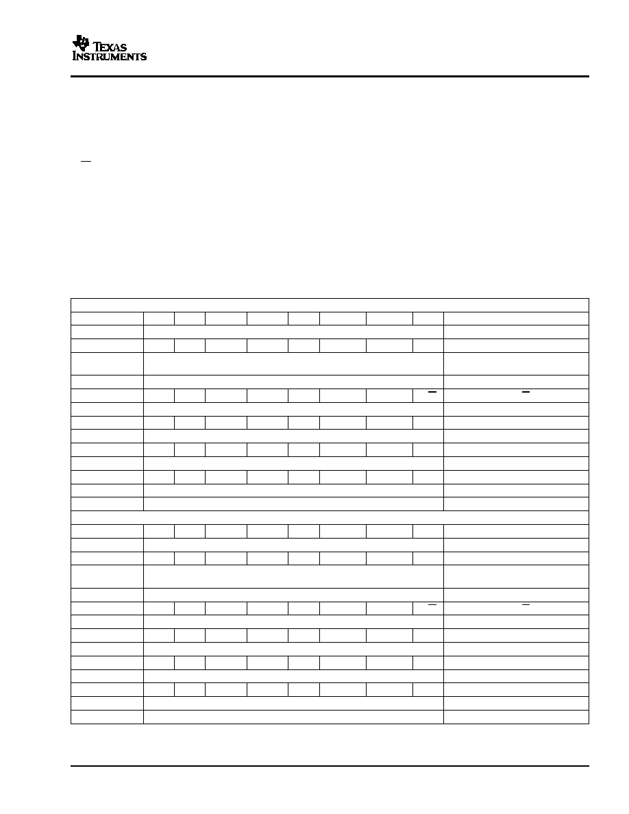
Control Byte
MSB
LSB
A3
A2
L1
L0
X
Sel1
Sel0
PD0
Table 1. Control Register Bit Descriptions
Bit Name
Bit Number/Description
A3
Extended Address Bit
The state of these bits must match the state of pins A3 and A2 in order for a
proper DAC8574 data update, except in broadcast update mode.
A2
Extended Address Bit
L1
Load1 (Mode Select) Bit
Are used for selecting the update mode.
L2
Load0 (Mode Select) Bit
00
Store I
2
C data. The contents of MS-BYTE and LS-BYTE (or power down information) are stored in the
temporary register of a selected channel. This mode does not change the DAC output of the selected
channel.
01
Update selected DAC with I
2
C data. Most commonly utilized mode. The contents of MS-BYTE and
LS-BYTE (or power down information) are stored in the temporary register and in the DAC register of
the selected channel. This mode changes the DAC output of the selected channel with the new data.
10
4-Channel synchronous update. The contents of MS-BYTE and LS-BYTE (or power down information)
are stored in the temporary register and in the DAC register of the selected channel. Simultaneously,
the other three channels get updated with previously stored data from the temporary register. This
mode updates all four channels together.
11
Broadcast update mode. This mode has two functions. In broadcast mode, DAC8574 responds
regardless of local address matching, and channel selection becomes irrelevant as all channels update.
This mode is intended to enable up to 64 channels simultaneous update, if used with the I
2
C broadcast
address (1001 0000).
If Sel1=0
All four channels are updated with the contents of their temporary register
data.
If Sel1=1
All four channels are updated with the MS-BYTE and LS-BYTE data or
powerdown.
Sel1
Buff Sel1 Bit
Channel Select Bits
Sel0
Buff Sel0 Bit
00
Channel A
01
Channel B
10
Channel C
11
Channel D
PD0
Power Down Flag
0
Normal operation
1
Power-down flag (MSB7 and MSB6 indicate a power-down operation, as shown in Table 2).
18
www.ti.com
DAC8574
SLAS377A ≠ JANUARY 2003 ≠ REVISED JUNE 2003
Table 2. Control Byte
C7
C6
C5
C4
C3
C2
C1
C0
MSB7
MSB6
MSB5...
Don't
MSB
MSB-1
MSB-2
A3
A2
Load1
Load0
Ch Sel 1
Ch Sel 0
PD0
Care
(PD1)
(PD2)
...LSB
DESCRIPTION
(Address Sel-
ect)
(A3 and A2
Write to temporary
should corre-
0
0
X
0
0
0
Data
register A (TRA) with
spond to the
data
package ad-
Write to temporary
dress set via
0
0
X
0
1
0
Data
register B (TRB) with
pins A3 and
data
A2.)
Write to temporary
0
0
X
1
0
0
Data
register C (TRC) with
data
Write to temporary
0
0
X
1
1
0
Data
register D (TRD) with
data
(00, 01, 10, or 11)
Write to TRx (selected
by C2 &C1
0
0
X
1
see Table 8
0
w/Powerdown Com-
mand
(00, 01, 10, or 11)
Write to TRx (selected
0
1
X
0
Data
by C2 &C1 and load
DACx w/data
(00, 01, 10, or 11)
Power-down DACx
0
1
X
1
see Table 8
0
(selected by C2 and
C1)
(00, 01, 10, or 11)
Write to TRx (selected
1
0
X
0
Data
by C2 &C1 w/ data and
load all DACs
(00, 01, 10, or 11)
Power-down DACx
1
0
X
1
see Table 8
0
(selected by C2 and
C1) & load all DACs
Broadcast Modes (controls up to 4 devices on a single serial bus)
Update all DACs, all
X
X
1
1
X
0
X
X
X
devices with previously
stored TRx data
Update all DACs, all
X
X
1
1
X
1
X
0
Data
devices with MSB[7:0]
and LSB[7:0] data
Power-down all DACs,
X
X
1
1
X
1
X
1
see Table 8
0
all devices
Most Significant Byte
Most Significant Byte MSB[7:0] consists of eight most significant bits of 16-bit unsigned binary D/A conversion
data. C0=1, MSB[7], MSB[6] indicate a powerdown operation as shown in Table 8.
Least Significant Byte
Least Significant Byte LSB[7:0] consists of the 8 least significant bits of the 16bit unsigned binary D/A conversion
data. DAC8574 updates at the falling edge of the acknowledge signal that follows the LSB[0] bit.
Default Readback Condition
If the user initiates a readback of a specified channel without first writing data to that specified channel, the
default readback is all zeros, since the readback register is initialized to 0 during the power on reset phase.
19
www.ti.com
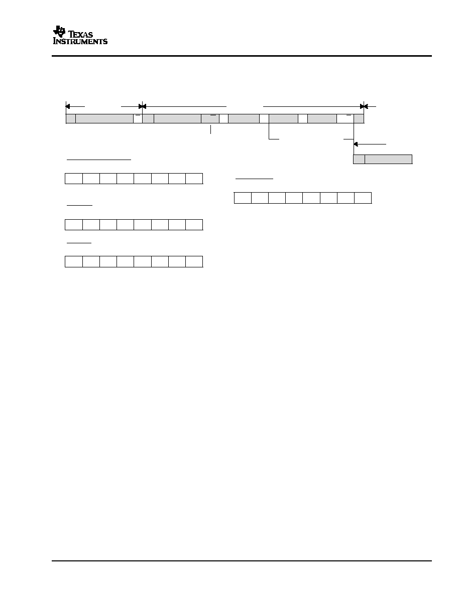
SLAVE ADDRESS R/W
A Ctrl-Byte
A MS-Byte A
LS-Byte
A/A
P
"0" (write)
Data Transferred
(n* Words + Acknowledge)
Word = 16 Bit
From Master to DAC8574
From DAC8574 to Master
A = Acknowledge (SDA LOW)
A = Not Acknowledge (SDA HIGH)
S = START Condition
Sr = Repeated START Condition
P = STOP Condition
DAC8574 I
2
C-SLAVE ADDRESS:
1
0
0
1
1
A1
A0
R/W
MSB
LSB
Factory Preset
A0 = I
2
C Address Pin
A1 = I
2
C Address Pin
S
`0' = Write to DAC8574
`1' = Read from DAC8574
DAC8574
SLAS377A ≠ JANUARY 2003 ≠ REVISED JUNE 2003
LDAC Functionality
Depending on the control byte, DACs are synchronously updated on the falling edge of the acknowledge signal
that follows LS byte. The LDAC pin is required only when an external timing signal is used to update all the
channels of the DAC asynchronously. LDAC is a positive edge triggered asynchronous input that allows four
DAC output voltages to be updated simultaneously with temporary register data. The LDAC trigger should only
be used after the buffers temporary registers are properly updated through software.
DAC8574 Registers
Table 3. DAC8574 Architecture Register Descriptions
Register
Description
CTRL[7:0]
Stores 8-bit wide control byte sent by the master
Stores the 8 most significant bits of unsigned binary data sent by the master. Can also store 2-bit
MSB[7:0]
power-down data.
LSB[7:0]
Stores the 8 least significant bits of unsigned binary data sent by the master.
TRA[17:0], TRB[17:0],
18-bit temporary storage registers assigned to each channel. Two MSBs store power-down information, 16
TRC[17:0], TRD[17:0]
LSBs store data.
DRA[17:0], DRB[17:0],
18-bit DAC registers for each channel. Two MSBs store power-down information, 16 LSBs store DAC data.
DRC[17:0], DRD[17:0]
An update of this register means a DAC update with data or power-down.
DAC8574 as a Slave Receiver - Standard and Fast Mode
Figure 51 shows the standard and fast mode master transmitter addressing a DAC8574 Slave Receiver with a
7-bit address.
Figure 51. Standard and Fast Mode: Slave Receiver
20
www.ti.com
HS-Master Code
R/W
A Ctrl-Byte
A MS-Byte A
LS-Byte
A/A
P
"0" (write)
Data Transferred
(n* Words + Acknowledge)
Word = 16 Bit
S
A Sr Slave Address
HS-Mode Continues
F/S-Mode
HS-Mode
F/S-Mode
Sr Slave Address
0
0
0
0
1
X
X
R/X
MSB
LSB
HS-Mode Master Code:
A3
A2
L1
L0
X
Sel1 Sel2 PD0
MSB
LSB
Control Byte:
A3
= Extended Address Bit
A2
= Extended Address Bit
L1
= Load1 (Mode Select) Bit
L0
= Load0 (Mode Select) Bit
Sel1 = Buff Sel1 (Channel) Select Bit
Sel0 = Buff Sel0 (Channel) Select Bit
PD0 = Power Down Flag
D15
D14
D13
D12
D11
D10
D9
D8
MSB
LSB
MS-Byte:
D7
D6
D5
D4
D3
D2
D1
D0
MSB
LSB
LS-Byte:
D15 - D0 = Data Bits
X = Don't Care
DAC8574
SLAS377A ≠ JANUARY 2003 ≠ REVISED JUNE 2003
DAC8574 as a Slave Receiver - High-Speed Mode
Figure 52 shows the high-speed mode master transmitter addressing a DAC8574 Slave Receiver with a 7-bit
address.
Figure 52. High-Speed Mode: Slave Receiver
21

www.ti.com
DAC8574
SLAS377A ≠ JANUARY 2003 ≠ REVISED JUNE 2003
Master Transmitter Writing to a Slave Receiver (DAC8574) in Standard/Fast Modes
All write access sequences begin with the device address (with R/W = 0) followed by the control byte. This
control byte specifies the operation mode of DAC8574 and determines which channel of DAC8574 is being
accessed in the subsequent read/write operation. The LSB of the control byte (PD0-Bit) determines if the
following data is power-down data or regular data.
With (PD0-Bit = 0) the DAC8574 expects to receive data in the following sequence HIGH-BYTE ≠LOW-BYTE ≠
HIGH-BYTE ≠ LOW-BYTE
..., until a STOP Condition or REPEATED START Condition on the I
2
C-Bus is
recognized (refer to the DATA INPUT MODE section of Table 4).
With (PD0-Bit = 1) the DAC8574 expects to receive 2 Bytes of power-down data (refer to the POWER DOWN
MODE section of Table 4).
Table 4. Write Sequence in F/S Mode
DATA INPUT MODE
Transmitter
MSB
6
5
4
3
2
1
LSB
Comment
Master
Start
Begin sequence
Master
1
0
0
1
1
A1
A0
R/W
Write addressing (R/W=0)
DAC8574
DAC8574 Acknowledges
Master
A3
A2
Load 1
Load 0
x
Buff Sel 1
Buff Sel 0
PD0
Control byte (PD0=0)
DAC8574
DAC8574 Acknowledges
Master
D15
D14
D13
D12
D11
D10
D9
D8
Writing data word, high byte
DAC8574
DAC8574 Acknowledges
Master
D7
D6
D5
D4
D3
D2
D1
D0
Writing data word, low byte
DAC8574
DAC8574 Acknowledges
Master
Data or Stop or Repeated Start (1)
Data or done (2)
POWER DOWN MODE
Transmitter
MSB
6
5
4
3
2
1
LSB
Comment
Master
Start
Begin sequence
Master
1
0
0
1
1
A1
A0
R/W
Write addressing (R/W=0)
DAC8574
DAC8574 Acknowledges
Master
A3
A2
Load 1
Load 0
x
Buff Sel 1
Buff Sel 0
PD0
Control byte (PD0 = 1)
DAC8574
DAC8574 Acknowledges
Master
PD1
PD2
0
0
0
0
0
0
Writing data word, high byte
DAC8574
DAC8574 Acknowledges
Master
0
0
0
0
0
0
0
0
Writing data word, low byte
DAC8574
DAC8574 Acknowledges
Master
Stop or Repeated Start (1)
Done
(1)
Use repeated START to secure bus operation and loop back to the stage of write addressing for next Write.
(2)
Once DAC8574 is properly addressed and control byte is sent, HIGH≠BYTE≠LOW≠BYTE sequences can repeat until a STOP
condition or repeated START condition is received.
22
www.ti.com
DAC8574
SLAS377A ≠ JANUARY 2003 ≠ REVISED JUNE 2003
Master Transmitter Writing to a Slave Receiver (DAC8574) in HS Mode
When writing data to the DAC8574 in HS-mode, the master begins to transmit what is called the HS-Master
Code
(0000 1XXX) in F/S-mode. No device is allowed to acknowledge the HS-Master Code, so the HS-Master
Code
is followed by a NOT acknowledge.
The master then switches to HS-mode and issues a repeated start condition, followed by the address byte (with
R/W = 0) after which the DAC8574 acknowledges by pulling SDA low. This address byte is usually followed by
the control byte, which is also acknowledged by the DAC8574. The LSB of the control byte (PD0-Bit) determines
if the following data is power-down data or regular data.
With (PD0-Bit = 0) the DAC8574 expects to receive data in the following sequence HIGH-BYTE ≠ LOW-BYTE ≠
HIGH-BYTE ≠ LOW-BYTE...., until a STOP condition or repeated start condition on the I
2
C-Bus is recognized
(refer to Table 5 HS-MODE WRITE SEQUENCE - DATA).
With (PD0-Bit = 1) the DAC8574 expects to receive 2 bytes of power-down data (refer to Table 5 HS-MODE
WRITE SEQUENCE - POWER DOWN).
Table 5. Master Transmitter Writes to Slave Receiver (DAC8574) in HS-Mode
HS MODE WRITE SEQUENCE - DATA
Transmitter
MSB
6
5
4
3
2
1
LSB
Comment
Master
Start
Begin sequence
Master
0
0
0
0
1
X
X
X
HS Mode Master Code
No device may acknowledge HS
NONE
Not Acknowledge
master code
Master
Repeated Start
Master
1
0
0
1
1
A1
A0
R/W
Write addressing (R/W=0)
DAC8574
DAC8574 Acknowledges
Master
0
0
Load 1
Load 0
0
Buff Sel 1
Buff Sel 0
PD0
Control byte (PD0=0)
DAC8574
DAC8574 Acknowledges
Master
D15
D14
D13
D12
D11
D10
D9
D8
Writing data word, MSB
DAC8574
DAC8574 Acknowledges
Master
D7
D6
D5
D4
D3
D2
D1
D0
Writing data word, LSB
DAC8574
DAC8574 Acknowledges
Master
Data or Stop or Repeated Start (1)
Data or done (2)
HS MODE WRITE SEQUENCE - POWER DOWN
Transmitter
MSB
6
5
4
3
2
1
LSB
Comment
Master
Start
Begin sequence
Master
0
0
0
0
1
X
X
X
HS Mode Master Code
No device may acknowledge HS
NONE
Not Acknowledge
master code
Master
Repeated Start
Master
1
0
0
1
1
A1
A0
R/W
Write addressing (R/W = 0)
DAC8574
DAC8574 Acknowledges
Master
0
0
Load 1
Load 2
0
Buff Sel 1
Buff Sel 0
PD0
Control Byte (PD0=1)
DAC8574
DAC8574 Acknowledges
Master
PD1
PD2
0
0
0
0
0
0
Writing data word, high byte
DAC8574
DAC8574 Acknowledges
Master
0
0
0
0
0
0
0
0
Writing data word, low byte
DAC8574
DAC8574 Acknowledges
Master
Stop or repeated start (1)
Done
(1)
Use repeated start to secure bus operation and loop back to the stage of write addressing for next Write.
(2)
Once DAC8574 is properly addressed and control byte is sent, high-byte-low-byte sequences can repeat until a stop or repeated start
condition is received.
23
www.ti.com
SLAVE ADDRESS R/W
A Ctrl <7:1>
A
MS-Byte A
LS-Byte
A P
'0' (write)
Data Transferred
(2 Bytes + Acknowledge)
PDN-Byte:
PD1
PD2
1
1
1
1
1
1
MSB
LSB
S
PD0
Sr Slave Address
R/W A
'1' (read)
'0' = (Normal Mode)
A
PDN-Byte A
LS-Byte
A P
PD0
Sr Slave Address
R/W
A
MS-Byte A
(DAC8574)
(DAC8574)
(DAC8574)
(DAC8574)
(DAC8574)
(MASTER)
(MASTER)
'1' = (Power Down Flag)
Data Transferred
(3 Bytes + Acknowledge)
(DAC8574)
(MASTER)
(MASTER)
(MASTER)
PD1 = Power-Down Bit
PD2 = Power-Down Bit
'1' (read)
Slave Address
R/W A Ctrl <7:1>
A
MS-Byte A
LS-Byte
A P
'0' (write)
Data Transferred
(2 Bytes + Acknowledge)
PD0
Sr
Slave Address
R/W A
'1' (read)
'0' = (Normal Mode)
A
PDN-Byte A
LS-Byte
A P
PD0
Sr Slave Address
R/W
A
MS-Byte A
(DAC8574)
(DAC8574)
(DAC8574)
(MASTER)
(MASTER)
'1' = (Power -Down Flag)
Data Transferred
(3 Bytes + Acknowledge)
(DAC8574)
(MASTER)
(MASTER)
(MASTER)
Sr
HS-Mode
A
S
F/S-Mode
'1' (read)
HS-Master Code
DAC8574
SLAS377A ≠ JANUARY 2003 ≠ REVISED JUNE 2003
DAC8574 as a Slave Transmitter - Standard and Fast Mode
Figure 53 shows the standard and fast mode master transmitter addressing a DAC8574 Slave Transmitter with a
7-bit address.
Figure 53. Standard and Fast Mode: Slave Transmitter
DAC8574 as a Slave Transmitter - High-Speed Mode
Figure 54 shows an I
2
C-Master addressing DAC8574 in high-speed mode (with a 7-bit address), as a Slave
Transmitter
.
Figure 54. High-Speed Mode: Slave Transmitter
24

www.ti.com
DAC8574
SLAS377A ≠ JANUARY 2003 ≠ REVISED JUNE 2003
Master Receiver Reading From a Slave Transmitter (DAC8574) in Standard/Fast Modes
When reading data back from the DAC8574, the user begins with an address byte (with R/W = 0) after which the
DAC8574 will acknowledge by pulling SDA low. This address byte is usually followed by the Control Byte, which
is also acknowledged by the DAC8574. Following this there is a REPEATED START condition by the Master and
the address is resent with (R/W = 1). This is acknowledged by the DAC8574, indicating that it is prepared to
transmit data. Two or three bytes of data are then read back from the DAC8574, depending on the (PD0-Bit).
The value of Buff-Sel1 and Buff-Sel0 determines, which channel data is read back. A STOP Condition follows.
With the (PD0-Bit = 0) the DAC8574 transmits 2 bytes of data, HIGH-BYTE followed by the LOW-BYTE (refer to
Table 2. Data Readback Mode - 2 bytes).
With the (PD0-Bit = 1) the DAC8574 transmits 3 bytes of data, POWER-DOWN-BYTE followed by the
HIGH-BYTE
followed by the LOW-BYTE (refer to Table 2. Data Readback Mode - 3 bytes).
Table 6. Read Sequence in F/S Mode
DATA READBACK MODE - 2 BYTES
Transmitter
MSB
6
5
4
3
2
1
LSB
Comment
Master
Start
Begin sequence
Master
1
0
0
1
1
A1
A0
R/W
Write addressing (R/W=0)
DAC8574
DAC8574 Acknowledges
Master
A3
A2
Load 1
Load 0
x
Buff Sel 1
Buff Sel 0
PD0
Control byte (PD0=0)
DAC8574
DAC8574 Acknowledges
Master
Repeated Start
Master
1
0
0
1
1
A1
A0
R/W
Read addressing (R/W = 1)
DAC8574
DAC8574 Acknowledges
DAC8574
D15
D14
D13
D12
D11
D10
D9
D8
Reading data word, high byte
Master
Master Acknowledges
DAC8574
D7
D6
D5
D4
D3
D2
D1
D0
Reading data word, low byte
Master
Master Not Acknowledges
Master signal end of read
Master
Stop or Repeated Start (1)
Done
DATA READBACK MODE - 3 BYTES
Transmitter
MSB
6
5
4
3
2
1
LSB
Comment
Master
Start
Begin sequence
Master
1
0
0
1
1
A1
A0
R/W
Write addressing (R/W=0)
DAC8574
DAC8574 Acknowledges
Master
A3
A2
Load 1
Load 0
x
Buff Sel 1
Buff Sel 0
PD0
Control byte (PD0=1)
DAC8574
DAC8574 Acknowledges
Master
Repeated Start
Master
1
0
0
1
1
A1
A0
R/W
Read addressing (R/W = 1)
DAC8574
DAC8574 Acknowledges
DAC8574
PD1
PD2
1
1
1
1
1
1
Read power down byte
Master
Master Acknowledges
DAC8574
D15
D14
D13
D12
D11
D10
D9
D8
Reading data word, high byte
Master
Master Acknowledges
DAC8574
D7
D6
D5
D4
D3
D2
D1
D0
Reading data word, low byte
Master
Master Not Acknowledges
Master signal end of read
Master
Stop or Repeated Start (1)
Done
(1)
Use repeated start to secure bus operation and loop back to the stage of write addressing for next Write.
25

www.ti.com
DAC8574
SLAS377A ≠ JANUARY 2003 ≠ REVISED JUNE 2003
Master Receiver Reading From a Slave Transmitter (DAC8574) in HS-Mode
When reading data to the DAC8574 in HS-MODE, the master begins to transmit, what is called the HS-Master
Code
(0000 1XXX) in F/S-mode. No device is allowed to acknowledge the HS-Master Code, so the HS-Master
Code
is followed by a NOT acknowledge.
The Master then switches to HS-mode and issues a REPEATED START condition, followed by the address byte
(with R/W = 0) after which the DAC8574 acknowledges by pulling SDA low. This address byte is usually followed
by the control byte, which is also acknowledged by the DAC8574.
Then there is a REPEATED START condition initiated by the master and the address is resent with (R/W = 1).
This is acknowledged by the DAC8574, indicating that it is prepared to transmit data. Two or Three bytes of data
are then read back from the DAC8574, depending on the (PD0-Bit). The value of Buff-Sel1 and Buff-Sel0
determines, which channel data is read back. A STOP condition follows.
With the (PD0-Bit = 0) the DAC8574 transmits 2 bytes of data, HIGH-BYTE followed by LOW-BYTE (refer to
Table 7 HS-Mode Readback Sequence).
With the (PD0-Bit = 1) the DAC8574 transmits 3 bytes of data, POWER-DOWN-BYTE followed by the
HIGH-BYTE
followed by the LOW-BYTE (refer to Table 7 HS-Mode Readback Sequence).
Table 7. Master Receiver Reading Slave Transmitter (DAC8574) in HS-Mode
HS MODE READBACK SEQUENCE
Transmitter
MSB
6
5
4
3
2
1
LSB
Comment
Master
Start
Begin sequence
Master
0
0
0
0
1
X
X
X
HS Mode Master Code
No device may acknowledge HS
NONE
Not Acknowledge
master code
Master
Repeated Start
Master
1
0
0
1
1
A1
A0
R/W
Write addressing (R/W=0)
DAC8574
DAC8574 Acknowledges
Master
A3
A2
Load 1
Load 0
X
Buff Sel 1
Buff Sel 0
PD0
Control byte (PD0 = 1)
DAC8574
DAC8574 Acknowledges
Master
Repeated Start
Master
1
0
0
1
1
A1
A0
R/W
Read addressing (R/W=1)
DAC8574
DAC8574 Acknowledges
DAC8574
PD1
PD2
1
1
1
1
1
1
Power-down byte
Master
Master Acknowledges
DAC8574
D15
D14
D13
D12
D11
D10
D9
D8
Reading data word, high byte
Master
Master Acknowledges
DAC8574
D7
D6
D5
D4
D3
D2
D1
D0
Reading data word, low byte
Master
Master Not Acknowledges
Master signal end of read
Master
Stop or Repeated Start
Done
26
www.ti.com
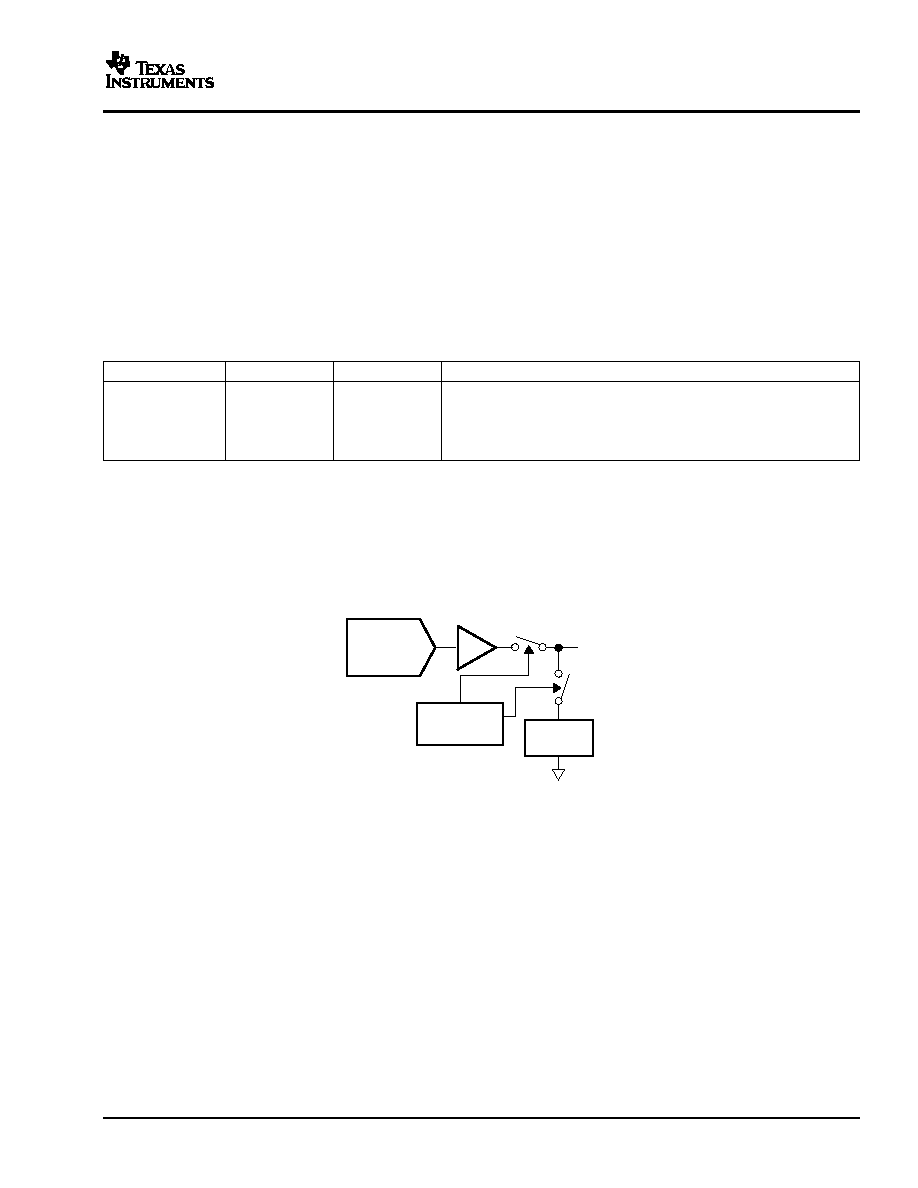
Resistor
String DAC
Powerdown
Circuitry
V
OUT
Amplifier
Resistor
Network
DAC8574
SLAS377A ≠ JANUARY 2003 ≠ REVISED JUNE 2003
Power-On Reset
The DAC8574 contains a power-on-reset circuit that controls the output voltage during power up. On power up,
the DAC register is filled with zeros and the output voltage is 0 V; it remains there until a valid write sequence is
made to the DAC. This is useful in applications where it is important to know the state of the output of the DAC
while it is in the process of powering up. No device pin should be brought high before supply is applied.
Power-Down Modes
The DAC8574 contains four separate power-down modes of operation. The modes are programmable via two
most significant bits of the MSB byte, while (CTRL[0] = PD0 = 1). Table 8 shows how the state of these bits
correspond to the mode of operation of the device.
Table 8. Power-Down Modes of Operation for the DAC8574
CTRL[0]
MSB[7]
MSB[6]
OPERATING MODE
1
0
0
High Impedance Output
1
0
1
1 k
to GND
1
1
0
100 k
to GND
1
1
1
High Impedance
When (CTRL[0] = PD0 = 0), the device works normally with its normal power consumption of 250 µA at 5 V per
channel. However, for the three power-down modes, the supply current falls to 200 nA at 5 V (50 nA at 3 V). Not
only does the supply current fall but also the output stage is also internally switched from the output of the
amplifier to a resistor network of known values. This has the advantage that the output impedance of the device
is known while in power-down mode. There are three different options: The output is connected internally to GND
through a 1 k
resistor, a 100 k resistor or left open-circuit (high impedance). The output stage is illustrated in
Figure 55.
Figure 55. Output Stage During Power Down
All linear circuitry is shut down when the power-down mode is activated. However, the contents of the DAC
register are unaffected when in power-down. The time to exit power down is typically 2.5 µs for V
DD
= 5 V and 5
µs for V
DD
= 3 V. (See the Typical Curves section for additional information.)
The DAC8574 offers a flexible power-down interface based on channel register operation. A channel consists of
a single 16 bit DAC with power-down circuitry, a temporary storage register (TR) and a DAC register (DR). TR
and DR are both 18 bits wide. Two MSBs represent the power-down condition and the 16 LSBs represent data
for TR and DR. By using bits 17 and 18 of TR and DR, a power-down condition can be temporarily stored and
used just like data. Internal circuits ensure that MSB[7] and MSB[6] get transferred to TR[17] and TR[16] (DR[17]
and DR[16]) when the power-down flag (CTRL[0] = PD0) is set. Therefore, DAC8574 treats power-down
conditions like data and all the operational modes are still valid for power down. It is possible to broadcast a
power-down condition to all the DAC8574s in the system, or it is possible to simultaneously power down a
channel while updating data on other channels.
27

www.ti.com
DAC8574
SLAS377A ≠ JANUARY 2003 ≠ REVISED JUNE 2003
CURRENT CONSUMPTION
The DAC8574 typically consumes 225 µA at V
DD
= 5 V and 200 µA at V
DD
= 3 V for each active channel,
including reference current consumption. Additional current consumption can occur at the digital inputs if V
IH
<<
V
DD
. For most efficient power operation, CMOS logic levels are recommended at the digital inputs to the DAC. In
power-down mode, typical current consumption is 200 nA. A delay time of 10 to 20 ms after a power-down
command is issued to the DAC is typically sufficient for the power-down current to drop below 10 µA.
DRIVING RESISTIVE AND CAPACITIVE LOADS
The DAC8574 output stage is capable of driving loads of up to 1000 pF while remaining stable. Within the offset
and gain error margins, the DAC8574 can operate rail-to-rail when driving a capacitive load. Resistive loads of 2
k
can be driven by the DAC8574 while achieving very good load regulation. Load regulation error increases as
the output voltage approaches each rail. When the outputs of the DAC are driven to the positive rail under
resistive loading, the PMOS transistor of each Class-AB output stage can enter into the linear region. When this
occurs, the added IR voltage drop deteriorates the linearity performance of the DAC. This only occurs within
approximately the top 20 mV of the DAC's digital input-to-voltage output transfer characteristic. The reference
voltage applied to the DAC8574 may be reduced below the supply voltage applied to V
DD
in order to eliminate
this condition if good linearity is a requirement at full scale (under resistive loading conditions).
CROSSTALK AND AC PERFORMANCE
The DAC8574 architecture uses separate resistor strings for each DAC channel in order to achieve ultra-low
crosstalk performance. DC crosstalk seen at one channel during a full-scale change on the neighboring channel
is typically less than 0.5 LSBs. The ac crosstalk measured (for a full-scale, 1 kHz sine wave output generated at
one channel, and measured at the remaining output channel) is typically under -100 dB. In addition, the
DAC8574 can achieve typical ac performance of 96 dB signal-to-noise ratio (SNR) and 65 dB total harmonic
distortion (THD), making the DAC8574 a solid choice for applications requiring high SNR at output frequencies at
or below 4 kHz.
OUTPUT VOLTAGE STABILITY
The DAC8574 exhibits excellent temperature stability of
±3 ppm/∞C typical output voltage drift over the specified
temperature range of the device. This enables the output voltage of each channel to stay within a
±25 µV window
for a
±1∞C ambient temperature change. Good power-supply rejection ratio (PSRR) performance reduces supply
noise present on V
DD
from appearing at the outputs to well below 10 µV-s. Combined with good dc noise
performance and true 16-bit differential linearity, the DAC8574 becomes a perfect choice for closed-loop control
applications.
SETTLING TIME AND OUTPUT GLITCH PERFORMANCE
Settling time to within the 16-bit accurate range of the DAC8574 is achievable within 10 µs for a full-scale code
change at the input. Worst case settling times between consecutive code changes is typically less than 2 µs. The
high-speed serial interface of the DAC8574 is designed in order to support up to 188ksps update rate. For
full-scale output swings, the output stage of each DAC8574 channel typically exhibits less than 100 mV of
overshoot and undershoot when driving a 200 pF capacitive load. Code-to-code change glitches are extremely
low (~10 µV) given that the code-to-code transition does not cross an Nx4096 code boundary. Due to internal
segmentation of the DAC8574, code-to-code glitches occur at each crossing of an Nx4096 code boundary.
These glitches can approach 100mVs for N = 15, but settle out within ~2 µs.
28
www.ti.com
8
6
4
9
5
7
1
2
3
12
14
11
10
13
16
15
DAC8574
V
OUTA
V
OUTB
V
REFH
V
DD
V
REFL
GND
V
OUTC
V
OUTD
A3
A2
A1
A0
IOV
DD
SDA
SCL
L
DAC
SDA
SCL
I
2
C Pullup Resistors
1 k
to 10 k
(typical)
IOV
DD
Microcontroller or
Microprocessor With
I
2
C Port
NOTE: DAC8574 power and input/output connections are omitted for clarity, except I
2
C Inputs.
DAC8574
SLAS377A ≠ JANUARY 2003 ≠ REVISED JUNE 2003
APPLICATION INFORMATION
The following sections give example circuits and tips for using the DAC8574 in various applications. For more
information, contact your local TI representative, or visit the Texas Instruments website at http://www.ti.com.
BASIC CONNNECTIONS
For many applications, connecting the DAC8574 is extremely simple. A basic connection diagram for the
DAC8574 is shown in Figure 56. The 0.1 µF bypass capacitors help provide the momentary bursts of extra
current needed from the supplies.
Figure 56. Typical DAC8574 Connections
The DAC8574 interfaces directly to standard mode, fast mode and high-speed mode I
2
C controllers. Any
microcontroller's I
2
C peripheral, including master-only and non-multiple-master I
2
C peripherals, work with the
DAC8574. The DAC8574 does not perform clock-stretching (i.e., it never pulls the clock line low), so it is not
necessary to provide for this unless other devices are on the same I
2
C bus.
Pullup resistors are necessary on both the SDA and SCL lines because I
2
C bus drivers are open-drain. The size
of the these resistors depend on the bus operating speed and capacitance on the bus lines. Higher-value
resistors consume less power, but increase the transition times on the bus, limiting the bus speed. Lower-value
resistors allow higher speed at the expense of higher power consumption. Long bus lines have higher
capacitance and require smaller pullup resistors to compensate. If the pullup resistors are too small the bus
drivers may not be able to pull the bus line low.
USING GPIO PORTS FOR I
2
C
Most microcontrollers have programmable input/output pins that can be set in software to act as inputs or
outputs. If an I
2
C controller is not available, the DAC8574 can be connected to GPIO pins, and the I
2
C bus
protocol simulated, or bit-banged, in software. An example of this for a single DAC8574 is shown in Figure 57.
29

www.ti.com
8
6
4
9
5
7
1
2
3
12
14
11
10
13
16
15
DAC8574
V
OUTA
V
OUTB
V
REFH
V
DD
V
REFL
GND
V
OUTC
V
OUTD
A3
A2
A1
A0
IOV
DD
SDA
SCL
L
DAC
GPIO-2
GPIO-1
IOV
DD
Microcontroller or
Microprocessor
NOTE: DAC8574 power and input/output connections are omitted for clarity, except I
2
C Inputs.
DAC8574
SLAS377A ≠ JANUARY 2003 ≠ REVISED JUNE 2003
APPLICATION INFORMATION (continued)
Figure 57. Using GPIO With a Single DAC8574
Bit-banging I
2
C with GPIO pins can be done by setting the GPIO line to zero and toggling it between input and
output modes to apply the proper bus states. To drive the line low, the pin is set to output a zero; to let the line
go high, the pin is set to input. When the pin is set to input, the state of the pin can be read; if another device is
pulling the line low, this reads as a zero in the port's input register.
Note that no pullup resistor is shown on the SCL line. In this simple case the resistor is not needed. The
microcontroller can simply leave the line on output, and set it to one or zero as appropriate. It can do this
because the DAC8574 never drives its clock line low. This technique can also be used with multiple devices, and
has the advantage of lower current consumption due to the absence of a resistive pullup.
If there are any devices on the bus that may drive their clock lines low, the above method should not be used.
The SCL line should be high-Z or zero, and a pullup resistor provided as usual. Note also that this cannot be
done on the SDA line in any case, because the DAC8574 drives the SDA line low from time to time, as all I
2
C
devices do.
Some microcontrollers have selectable strong pullup circuits built in to their GPIO ports. In some cases, these
can be switched on and used in place of an external pullup resistor. Weak pullups are also provided on some
microcontrollers, but usually these are too weak for I
2
C communication. Test any circuit before committing it to
production.
30
www.ti.com
REF02
15 V
5 V
950
m
A
V
DD
, V
ref
SCL
SDA
I
2
C
Interface
V
OUT
= 0 V to 5 V
DAC8574
DAC8574
SLAS377A ≠ JANUARY 2003 ≠ REVISED JUNE 2003
APPLICATION INFORMATION (continued)
USING REF02 AS A POWER SUPPLY FOR DAC8574
Due to the extremely low supply current required by the DAC8574, a possible configuration is to use a REF02 +5
V precision voltage reference to supply the required voltage to the DAC8574's supply input as well as the
reference input, as shown in Figure 58. This is especially useful if the power supply is quite noisy or if the system
supply voltages are at some value other than 5 V. The REF02 outputs a steady supply voltage for the DAC8574.
If the REF02 is used, the current it needs to supply to the DAC8574 is 950 µA typical and 1600 µA max for V
DD
=
5 V. When a DAC output is loaded, the REF02 also needs to supply the current to the load. The total typical
current required (with a 5 k
load on a single DAC output) is:
950 µA + (5 V / 5 k
) = 1.950 mA
The load regulation of the REF02 is typically 0.005%/mA, which results in an error of 488µV for 1.950-mA of
current drawn from it. This corresponds to a 6.4 LSB error for a 0 V to 5 V output range.
Figure 58. REF02 Power Supply
REF3040 can also be used to generate a 4.096-V reference from a 5-V supply.
31
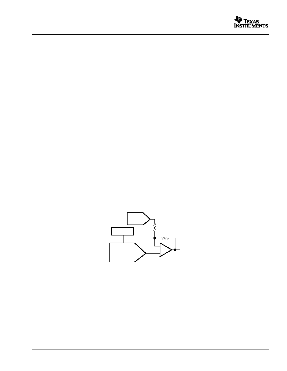
www.ti.com
DAC8574
V
REF
H
DAC7574
_
+
V
dac
R2
R1
REF3040
V
ref
V
tail
V
OUT
OPA4130
V
out
+
V
ref
R2
R1
)
1
Din
65536
≠V
tail
R2
R1
DAC8574
SLAS377A ≠ JANUARY 2003 ≠ REVISED JUNE 2003
APPLICATION INFORMATION (continued)
GENERATING
±5 V, ±10 V, and ± 12 V OUTPUTS FOR PRECISION INDUSTRIAL CONTROL
Industrial control applications can require multiple feedback loops consisting of sensors, ADCs, MCUs, DACs,
and actuators. Loop accuracy and loop speed are the two important parameters of such control loops.
Loop Accuracy:
In a control loop, the ADC has to be accurate. Offset, gain, and the integral linearity errors of the DAC are not
factors in determining the accuracy of the loop. As long as a voltage exists in the transfer curve of a monotonic
DAC, the loop can find it and settle to it. On the other hand, DAC resolution and differential linearity do determine
the loop accuracy, because each DAC step determines the minimum incremental change the loop can generate.
A DNL error less than -1 LSB (non-monotonicity) can create loop instability. A DNL error greater than +1 LSB
implies unnecessarily large voltage steps, and missed voltage targets. With high DNL errors, the loop looses its
stability, resolution, and accuracy. Offering 16-bit assured monotonicity and
± 0.25 LSB typical DNL error, 85XX
DACs are great choices for precision control loops.
Loop Speed:
Many factors determine control loop speed. Typically, the ADC's conversion time, and the MCU's computation
time are the two major factors that dominate the time contstant of the loop. DAC settling time is rarely a dominant
factor because ADC conversion times usually exceed DAC conversion times. DAC offset, gain, and linearity
errors can slow the loop down only during the start-up. Once the loop reaches its steady-state operation, these
errors do not affect loop speed any further. Depending on the ringing characteristics of the loop's transfer
function, DAC glitches can also slow the loop down. With its 188 ksps maximum data update rate, DAC8574 can
support high-speed control loops.
Generating Industrial Voltage Ranges:
For control loop applications, DAC gain and offset errors are not important parameters. This could be exploited to
lower trim and calibration costs in a high-voltage control circuit design. Using a quad op amp (OPA4130), a
voltage reference (REF3040) and a quad 12-bit DAC (DAC7574), the DAC8574 can generate the wide voltage
swings required by the control loop.
Figure 59. Low-cost, Wide-swing Voltage Generator for Control Loop Applications
The output voltage of the configuration is given by:
Fixed R1 and R2 resistors can be used to coarsely set the gain required in the first term of the equation. Once
R2 an R1 set the gain properly, a DAC7574 could be used to set the required offset voltages. Residual errors are
not an issue for loop accuracy because offset and gain errors could be tolerated.
For
±5-V operation: R1=10 k, R2 = 15 k, Vtail = 3.33 V, Vref = 4.096 V
For
±10-V operation: R1=10 k, R2 = 39 k, Vtail = 2.56 V, Vref = 4.096 V
For
±12-V operation: R1=10 k, R2 = 49 k, Vtail = 2.45 V, Vref = 4.096 V
32

www.ti.com
DAC8574
SLAS377A ≠ JANUARY 2003 ≠ REVISED JUNE 2003
APPLICATION INFORMATION (continued)
Digital Correction of DAC Errors
For open-loop applications requiring improved accuracy, offset and gain errors of the DAC8574 can be measured
and digitally corrected. To avoid waveform clipping, it is recommended to make the offset and gain error
measurements at codes 1024 and 64512 respectively. The total error of DAC8574 is dominated by gain and
offset errors, and it can be improved by an order of magnitude using the following digital correction:
DIN = DDIN ≠ OE ≠ (FSE ≠ OE)
◊ (DDIN ≠ 1024) ˜ 64512
where:
DIN = Digital input code to the DAC after offset and gain correction
DDIN = Digital input code to the DAC before offset and gain correction
OE = measured DAC error at code 1024 (in LSBs)
FSE = measured DAC error at code 64512 (in LSBs)
If division operation is not feasible, FSE measurement can be done at code 32768 instead of code 64512.
Division by 32768 implies a 15-bit arithmetic right shift. Improvements to the transfer curve are still significant.
DAC8574 integral linearity error is well within
±5 mV, therefore it only has a secondary effect on total DAC error.
Using piece-wise linear approximation, and non-volatile memory, integral linearity errors of DAC8574 can also be
digitally corrected. Consult TI applications engineering for details.
64 Channel Operation
DAC8574 is designed to facilitate high channel count operation. DAC8574 supports multichannel simultaneous
synchronous update up to 16 DAC8574 devices for up to 64 channels on a single I
2
C bus. Working with multiple
DAC8574s, single channel DAC8571s can be used on the same bus to obtain odd channel counts, or quad
channel DAC7574s can be used if some channels only need 12 bits of resolution.
Data or power down can be loaded to temporary registers of each channel serially and a single broadcast
operation can be used to update all channels of all devices simultaneously with previously stored data or
power-down condition. Another feature useful for system start-up or system shut-down is to broadcast the same
data (or power-down condition) to all channels with a single broadcast command.
All multichannel system updates are performed at the falling edge of the acknowledge signal that follows the
least significant byte.
The 64-channel operation requires 6-bit address decoding. 4-bit address decoding is used to support 16
DAC8574 devices on the same bus and 2-bit address decoding is used to select one out of four channels of a
DAC8574. 4-bit address decoding that selects one out of 16 DAC8574 devices is done as follows: To save I
2
C
address space, 2-bits (A0 and A1) are used for I
2
C address decoding, and two additional bits (A2 and A3) are
used for local address decoding. Up to 4 DAC8574 devices using the same I
2
C address can be connected on the
same I
2
C bus. These four devices with the same I
2
C address can be locally decoded using A2 and A3 pins. If
multiple devices use the same I
2
C address, multiple devices acknowledge at the same time. However, in order
for a particular device to respond to a command, the states of the first two bits of the control word C7 and C6
must match the states of A3 and A2 pins. Four devices per I
2
C address and four distinct I
2
C addresses enable
16 devices on the same bus.
The four address pins should be set at power-up, and address bits must be set to match a particular device's
address pins. To decode up to 16 DAC8574 devices, the logic states of A3, A2, A1, A0 address pins and C7, C6,
A1, A0 address bits should be set as shown in Table 9.
33
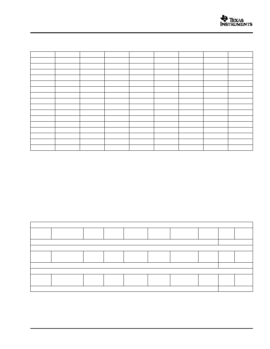
www.ti.com
DAC8574
SLAS377A ≠ JANUARY 2003 ≠ REVISED JUNE 2003
APPLICATION INFORMATION (continued)
Table 9. 64 Channel Address Decoding
DEV #
A3 PIN
C7 BIT
A2 PIN
C6 BIT
A1 PIN
A1 BIT
A0 PIN
A0 BIT
1
0
0
0
0
0
0
0
0
2
0
0
0
0
0
0
1
1
3
0
0
0
0
1
1
0
0
4
0
0
0
0
1
1
1
1
5
0
0
1
1
0
0
0
0
6
0
0
1
1
0
0
1
1
7
0
0
1
1
1
1
0
0
8
0
0
1
1
1
1
1
1
9
1
1
0
0
0
0
0
0
10
1
1
0
0
0
0
1
1
11
1
1
0
0
1
1
0
0
12
1
1
0
0
1
1
1
1
13
1
1
1
1
0
0
0
0
14
1
1
1
1
0
0
1
1
15
1
1
1
1
1
1
0
0
16
1
1
1
1
1
1
1
1
Once a DAC8574 device is selected, channel select bits C2 and C1 can select a particular channel. Overall, I
2
C
address bits A1, A0, control bits C7, C6, C2 and C1 form the 6-bit address required to select one channel out of
64 possibilities.
Broadcast operation is supported for both I
2
C addressing and for extended addressing. A broadcast address
(10010000) makes all DAC8574 devices listen, regardless of the states of A0 and A1 pins. Also, a broadcast
command (C5 = C4 = 1) makes all devices listen, regardless of the states of A2 and A3 pins. The same
broadcast command (C5 = C4 = 1) also selects all channels for a given device, regardless of the states of
channel select bits. Thus, a global broadcast message that simultaneously updates up to 64 channels uses
10010000 as I
2
C address and has (C5 = C4 = 1) in the control word.
Examples
I
2
C Standard and Fast Mode Examples (A0, A1, A2, A3 and LDAC pins tied to GND):
EXAMPLE 1: WRITE 1/4 SCALE TO CHANNEL A
ADDRESS [7...0]
C [7...0]
M [7...0]
L [7...0]
START
1001 1000
ACK
0001 0000
ACK
0100 0000
ACK
0000 0000
ACK
STOP
Previous VoutA output voltage is valid
VoutA = 1.25 V
EXAMPLE 2: WRITE 1/2 SCALE TO CHANNEL B
ADDRESS [7...0]
C [7...0]
M [7...0]
L [7...0]
START
1001 1000
ACK
0001 0010
ACK
0100 0000
ACK
0000 0000
ACK
STOP
Previous VoutB output voltage is valid
VoutB = 2.50 V
EXAMPLE 3: WRITE 3/4 SCALE TO CHANNEL C
ADDRESS [7...0]
C [7...0]
M [7...0]
L [7...0]
START
1001 1000
ACK
0001 0100
ACK
1100 0000
ACK
0000 0000
ACK
STOP
Previous VoutC output voltage is valid
VoutC = 3.75 V
34
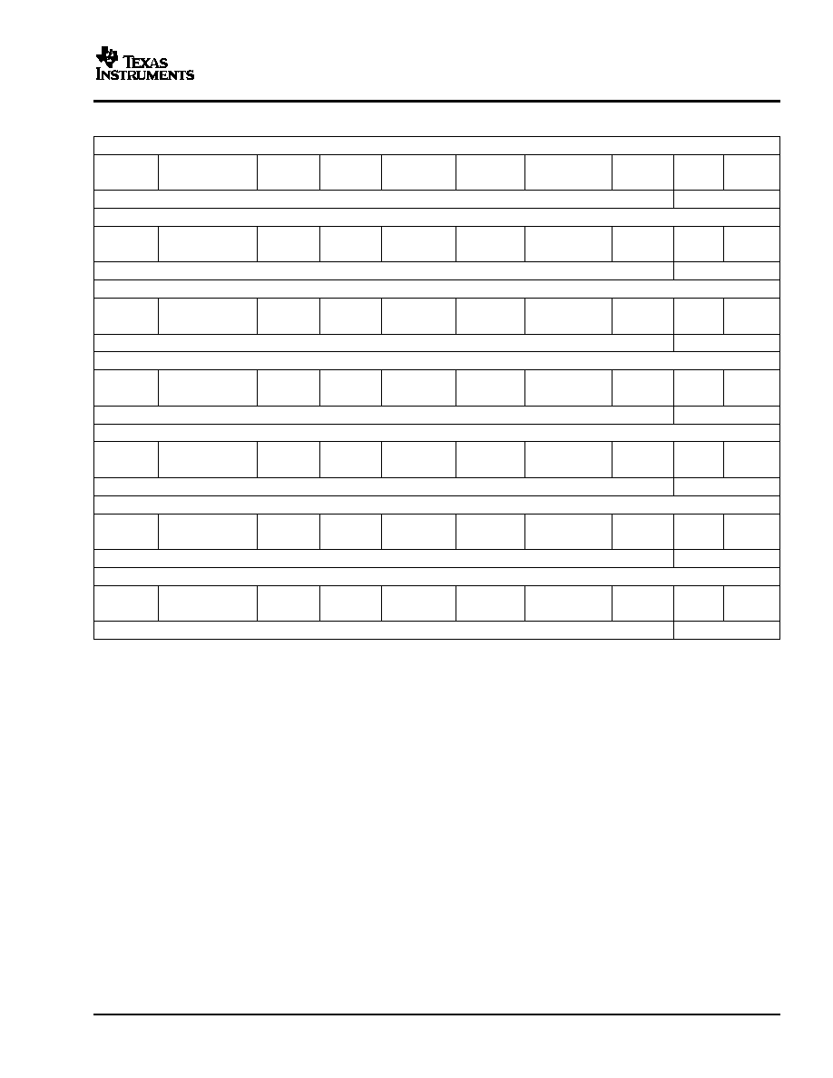
www.ti.com
DAC8574
SLAS377A ≠ JANUARY 2003 ≠ REVISED JUNE 2003
APPLICATION INFORMATION (continued)
EXAMPLE 4: WRITE 4/4 SCALE TO CHANNEL D
ADDRESS [7...0]
C [7...0]
M [7...0]
L [7...0]
START
1001 1000
ACK
0001 0110
ACK
1111 1111
ACK
1111 1111
ACK
STOP
Previous VoutD output voltage is valid
VoutB = 5.0 V
EXAMPLE 5: Power-Down Channel A, With Hi-Z Output
ADDRESS [7...0]
C [7...0]
M [7...0]
L [7...0]
START
1001 1000
ACK
0001 0101
ACK
0000 0000
ACK
0000 0000
ACK
STOP
Previous VoutA output voltage is valid
VoutA = Hi-Z
EXAMPLE 6: Power-Down Channel B, With Hi-Z Output
ADDRESS [7...0]
C [7...0]
M [7...0]
L [7...0]
START
1001 1000
ACK
0001 0011
ACK
0000 0000
ACK
0000 0000
ACK
STOP
Previous VoutB output voltage is valid
VoutB = Hi-Z
EXAMPLE 7: Power-Down Channel C, With Hi-Z Output
ADDRESS [7...0]
C [7...0]
M [7...0]
L [7...0]
START
1001 1000
ACK
0001 0101
ACK
0000 0000
ACK
0000 0000
ACK
STOP
Previous VoutC output voltage is valid
VoutC = Hi-Z
EXAMPLE 8: Power-Down Channel D, With Hi-Z Output
ADDRESS [7...0]
C [7...0]
M [7...0]
L [7...0]
START
1001 1000
ACK
0001 0111
ACK
0000 0000
ACK
0000 0000
ACK
STOP
Previous VoutD output voltage is valid
VoutD = Hi-Z
EXAMPLE 9: Power-Down Channel D, With 1 k
Output Impedance to Ground
ADDRESS [7...0]
C [7...0]
M [7...0]
L [7...0]
START
1001 1000
ACK
0001 0111
ACK
0100 0000
ACK
0000 0000
ACK
STOP
Previous VoutA output voltage is valid
VoutD = 0 V
EXAMPLE 10: Power-Down Channel D, With 100 k
Output Impedance to Ground
ADDRESS [7...0]
C [7...0]
M [7...0]
L [7...0]
START
1001 1000
ACK
0001 0111
ACK
1000 0000
ACK
0000 0000
ACK
STOP
Previous VoutD output voltage is valid
VoutD = 0 V
35
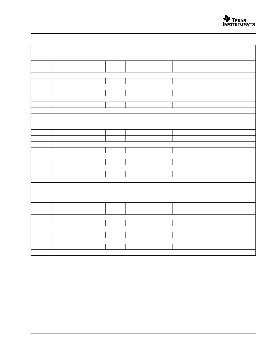
www.ti.com
DAC8574
SLAS377A ≠ JANUARY 2003 ≠ REVISED JUNE 2003
APPLICATION INFORMATION (continued)
EXAMPLE 11: Simultaneous Update of All Channels
Write 4/4 Scale, 4/3 Scale, 2/4 Scale, and 1/4 Scale Data to Temporary Registers of Channels A, B, C, D Serially, and Update all
DACs Simultaneously
ADDRESS [7...0]
C [7...0]
M [7...0]
L [7...0]
START
1001 1000
ACK
0000 0000
ACK
1111 1111
ACK
1111 1111
ACK
STOP
Previous DAC output voltages are valid for all channels
START
1001 1000
ACK
0000 0010
ACK
1100 0000
ACK
0000 0000
ACK
Previous DAC output voltages are valid for all channels
START
1001 1000
ACK
0000 0100
ACK
1000 0000
ACK
0000 0000
ACK
Previous DAC output voltages are valid for all channels
START
1001 1000
ACK
0010 0110
ACK
0100 0000
ACK
0000 0000
ACK
Previous DAC output voltages are valid for all channels
New data is valid
EXAMPLE 12: Simultaneous Update Channels A, B, C and Power-Down of Channel D at The End of The Fourth Cycle
Write 1/4 Scale, 2/4 Scale, 3/4 Scale, and Power-Down (Hi-Z) Data to Temporary Registers of Channels A, B, C, D Serially, and
Update Simultaneously
ADDRESS [7...0]
C [7...0]
M [7...0]
L [7...0]
START
1001 1000
ACK
0000 0000
ACK
1111 1111
ACK
1111 1111
ACK
STOP
Previous DAC output voltages are valid for all channels
START
1001 1000
ACK
0000 0010
ACK
1100 0000
ACK
0000 0000
ACK
STOP
Previous DAC output voltages are valid for all channels
START
1001 1000
ACK
0000 0100
ACK
1000 0000
ACK
0000 0000
ACK
STOP
Previous DAC output voltages are valid for all channels
START
1001 1000
ACK
0010 0110
ACK
0100 0000
ACK
0000 0000
ACK
STOP
Previous DAC output voltages are valid for all channels
New data is valid
EXAMPLE 13: Store data and wait for update command (Write codes 128, 256, 512, and 1024 to temporary registers of channels A,
B, C, D)
Write 4/4 Scale, 4/3 Scale, 2/4 Scale, and 1/4 Scale Data to Temporary Registers of Channels A, B, C, D Serially, and Update all
DACs Simultaneously
ADDRESS [7...0]
C [7...0]
M [7...0]
L [7...0]
START
1001 1000
ACK
0000 0000
ACK
0000 0000
ACK
1000 0000
ACK
STOP
Previous DAC output voltages are valid for all channels
START
1001 1000
ACK
0000 0010
ACK
0000 0001
ACK
0000 0000
ACK
STOP
Previous DAC output voltages are valid for all channels
START
1001 1000
ACK
0000 0100
ACK
0000 0010
ACK
0000 0000
ACK
STOP
Previous DAC output voltages are valid for all channels
START
1001 1000
ACK
0010 0110
ACK
0100 0100
ACK
0000 0000
ACK
STOP
Previous DAC output voltages are valid for all channels
36
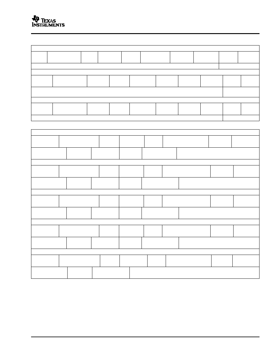
www.ti.com
DAC8574
SLAS377A ≠ JANUARY 2003 ≠ REVISED JUNE 2003
APPLICATION INFORMATION (continued)
EXAMPLE 14: Broadcast update command. All channels of all DAC8574s update with previously stored temporary register data.
ADDRESS [7...0]
C [7...0]
M [7...0]
L [7...0]
START
1001 0000
ACK
0011 0000
ACK
XXXX XXXX
ACK
XXXX XXXX
ACK
STOP
Previous DAC output voltages are valid for all channels, all DAC8574s
New data is valid
EXAMPLE 15: Broadcast Data. All channels of all DAC8574s get set to code 7.
ADDRESS [7...0]
C [7...0]
M [7...0]
L [7...0]
START
1001 0000
ACK
0011 0001
ACK
0000 0000
ACK
0000 0111
ACK
STOP
All Vouts = 7 x 76
Previous DAC output voltages are valid for all channels, all DAC8574s
µV
EXAMPLE 16: Broadcast Power-Down. All channels of all DAC8574s get powered down with output impedance of 1 k
to ground.
ADDRESS [7...0]
C [7...0]
M [7...0]
L [7...0]
START
1001 0000
ACK
0011 0001
ACK
0100 0000
ACK
0000 0000
ACK
STOP
Previous DAC output voltages are valid for all channels, all DAC8574s
All Vouts = GND
I
2
C Read-back Examples (A0, A1, A2, A3 and LDAC pins tied to GND):
EXAMPLE 17: Read back channel A power-down bits and 16-bit channel A data. V denotes valid logic.
ADDRESS [7...0]
C [7...0]
REPEATED
ADDRESS
START
1001 1000
ACK
0001 0001
ACK
START
1001 1001
ACK
PWD [7...0]
MASTER
MSB [7...0]
MASTER
LSB [7...0]
MASTER
VV11 1111
ACK
VVVV VVVV
ACK
VVVV VVVV
NOT ACK
EXAMPLE 18: Read back channel B power-down bits and 16-bit channel B data. V denotes valid logic.
ADDRESS [7...0]
C [7...0]
REPEATED
ADDRESS
START
1001 1000
ACK
0001 0011
ACK
START
1001 1001
ACK
PWD [7...0]
MASTER
MSB [7...0]
MASTER
LSB [7...0]
MASTER
VV11 1111
ACK
VVVV VVVV
ACK
VVVV VVVV
NOT ACK
EXAMPLE 19: Read back channel C power-down bits and 16-bit channel C data. V denotes valid logic.
ADDRESS [7...0]
C [7...0]
REPEATED
ADDRESS
START
1001 1000
ACK
0001 0101
ACK
START
1001 1001
ACK
PWD [7...0]
MASTER
MSB [7...0]
MASTER
LSB [7...0]
MASTER
VV11 1111
ACK
VVVV VVVV
ACK
VVVV VVVV
NOT ACK
EXAMPLE 20: Read back channel D power-down bits and 16-bit channel D data. V denotes valid logic.
ADDRESS [7...0]
C [7...0]
REPEATED
ADDRESS
START
1001 1000
ACK
0001 0011
ACK
START
1001 1001
ACK
PWD [7...0]
MASTER
MSB [7...0]
MASTER
LSB [7...0]
MASTER
VV11 1111
ACK
VVVV VVVV
ACK
VVVV VVVV
NOT ACK
EXAMPLE 21: Read back 16-bit channel D data only. V denotes valid logic.
ADDRESS [7...0]
C [7...0]
REPEATED
ADDRESS
START
1001 1000
ACK
0001 0110
ACK
START
1001 1001
ACK
MSB [7...0]
MASTER
LSB [7...0]
MASTER
VVVV VVVV
ACK
VVVV VVVV
NOT ACK
37
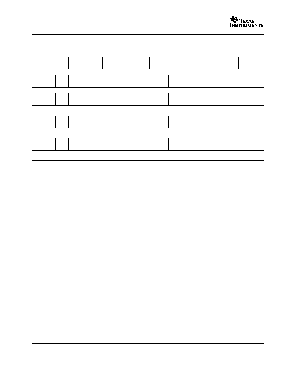
www.ti.com
DAC8574
SLAS377A ≠ JANUARY 2003 ≠ REVISED JUNE 2003
APPLICATION INFORMATION (continued)
I
2
C High Speed Examples (A0, A1, A2, A3 and LDAC pins tied to GND):
EXAMPLE 22: Ramp generation on channel D (Up to Code 7 is shown)
HS Master Code
NOT
REPEATED
ADDRESS
C [7
... 0]
START
0001 0000
ACK
START
10011 0000
ACK
0001 0110
ACK
Previous VoutD voltage valid
MSB [7
...0]
LSB [7
...0]
MSB [7
...0]
LSB [7
...0]
0000 0000
ACK
0000 0000
ACK
0000 0000
ACK
0000 0001
ACK
Previous VoutD voltage valid
VoutD = 0 V
VoutD = 76 µV
MSB [7
...0]]
LSB [7
...0]
MSB 7
...0]
LSB [7
...0]
0000 0000
ACK
0000 0010
ACK
0000 0000
ACK
0000 0011
ACK
VoutD = 76 µV
VoutD = 2 x 76 µV
VoutD = 3 x 76
µV
MSB [7
...0]
LSB [7
...0]
MSB [7
...0]
LSB [7
...0]
0000 0000
ACK
0000 0100
ACK
0000 0000
ACK
0000 0101
ACK
VoutD = 3 x 76 µV
VoutD = 4 x 76 µV
VoutD = 5 x 76
µV
MSB [7
...0]
LSB [7
...0]
MSB [7
...0]
LSB [7
...0]
0000 0000
ACK
0000 0110
ACK
0000 0000
ACK
0000 0111
ACK
VoutD = 5 x 76 µV
VoutD = 6 x 76 µV
VoutD = 7 x 76
µV
LAYOUT
A precision analog component requires careful layout, adequate bypassing, and clean, well-regulated power
supplies.
The power applied to V
DD
should be well-regulated and low noise. Switching power supplies and dc/dc
converters often have high-frequency glitches or spikes riding on the output voltage. In addition, digital
components can create similar high-frequency spikes as their internal logic switches states. This noise can easily
couple into the DAC output voltage through various paths between the power connections and analog output.
As with the GND connection, V
DD
should be connected to a positive power-supply plane or trace that is separate
from the connection for digital logic until they are connected at the power-entry point. In addition, a 1 µF to 10 µF
capacitor in parallel with a 0.1 µF bypass capacitor is strongly recommended. In some situations, additional
bypassing may be required, such as a 100 µF electrolytic capacitor or even a Pi filter made up of inductors and
capacitors--all designed to essentially low-pass filter the ≠5 V supply, removing the high-frequency noise.
38
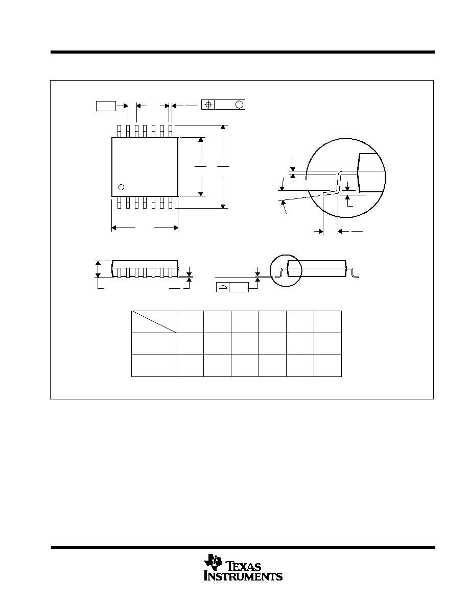
MECHANICAL DATA
MTSS001C ≠ JANUARY 1995 ≠ REVISED FEBRUARY 1999
1
POST OFFICE BOX 655303
∑
DALLAS, TEXAS 75265
PW (R-PDSO-G**)
PLASTIC SMALL-OUTLINE PACKAGE
14 PINS SHOWN
0,65
M
0,10
0,10
0,25
0,50
0,75
0,15 NOM
Gage Plane
28
9,80
9,60
24
7,90
7,70
20
16
6,60
6,40
4040064/F 01/97
0,30
6,60
6,20
8
0,19
4,30
4,50
7
0,15
14
A
1
1,20 MAX
14
5,10
4,90
8
3,10
2,90
A MAX
A MIN
DIM
PINS **
0,05
4,90
5,10
Seating Plane
0
∞
≠ 8
∞
NOTES: A. All linear dimensions are in millimeters.
B. This drawing is subject to change without notice.
C. Body dimensions do not include mold flash or protrusion not to exceed 0,15.
D. Falls within JEDEC MO-153

IMPORTANT NOTICE
Texas Instruments Incorporated and its subsidiaries (TI) reserve the right to make corrections, modifications,
enhancements, improvements, and other changes to its products and services at any time and to discontinue
any product or service without notice. Customers should obtain the latest relevant information before placing
orders and should verify that such information is current and complete. All products are sold subject to TI's terms
and conditions of sale supplied at the time of order acknowledgment.
TI warrants performance of its hardware products to the specifications applicable at the time of sale in
accordance with TI's standard warranty. Testing and other quality control techniques are used to the extent TI
deems necessary to support this warranty. Except where mandated by government requirements, testing of all
parameters of each product is not necessarily performed.
TI assumes no liability for applications assistance or customer product design. Customers are responsible for
their products and applications using TI components. To minimize the risks associated with customer products
and applications, customers should provide adequate design and operating safeguards.
TI does not warrant or represent that any license, either express or implied, is granted under any TI patent right,
copyright, mask work right, or other TI intellectual property right relating to any combination, machine, or process
in which TI products or services are used. Information published by TI regarding third-party products or services
does not constitute a license from TI to use such products or services or a warranty or endorsement thereof.
Use of such information may require a license from a third party under the patents or other intellectual property
of the third party, or a license from TI under the patents or other intellectual property of TI.
Reproduction of information in TI data books or data sheets is permissible only if reproduction is without
alteration and is accompanied by all associated warranties, conditions, limitations, and notices. Reproduction
of this information with alteration is an unfair and deceptive business practice. TI is not responsible or liable for
such altered documentation.
Resale of TI products or services with statements different from or beyond the parameters stated by TI for that
product or service voids all express and any implied warranties for the associated TI product or service and
is an unfair and deceptive business practice. TI is not responsible or liable for any such statements.
Following are URLs where you can obtain information on other Texas Instruments products and application
solutions:
Products
Applications
Amplifiers
amplifier.ti.com
Audio
www.ti.com/audio
Data Converters
dataconverter.ti.com
Automotive
www.ti.com/automotive
DSP
dsp.ti.com
Broadband
www.ti.com/broadband
Interface
interface.ti.com
Digital Control
www.ti.com/digitalcontrol
Logic
logic.ti.com
Military
www.ti.com/military
Power Mgmt
power.ti.com
Optical Networking
www.ti.com/opticalnetwork
Microcontrollers
microcontroller.ti.com
Security
www.ti.com/security
Telephony
www.ti.com/telephony
Video & Imaging
www.ti.com/video
Wireless
www.ti.com/wireless
Mailing Address:
Texas Instruments
Post Office Box 655303 Dallas, Texas 75265
Copyright
2003, Texas Instruments Incorporated