
www.ti.com
PRODUCT PREVIEW
FEATURES
DESCRIPTION
APPLICATIONS
16
DAC
D0
D1
D2
D3
D4
D5
D6
D7
D8
D9
D10
D11
D12
D13
D14
D15
A0
A1
EN
A
B
C
D
2:4
Decode
SDO
SDI
CS
CLK
DGND
RS
MSB
LDAC
V
SS
A
GND
F
A
GND
D
I
OUT
D
R
FB
D
A
GND
C
I
OUT
C
R
FB
C
A
GND
B
I
OUT
C
R
FB
B
A
GND
A
I
OUT
A
R
FB
A
A B C D
V
REF
Input
Register
R
Input
Register
R
Input
Register
R
Input
Register
R
Power-on
Reset
DAC A
Register
R
DAC B
Register
R
DAC C
Register
R
DAC D
Register
R
DAC A
DAC B
DAC C
DAC D
DAC8814
SBAS338 ≠ JANUARY 2005
Quad, Serial Input 16-Bit Multiplying Digital-to-Analog Converter
∑
Relative Accuracy: 1 LSB Max
The DAC8814 is a quad, 16-bit, current-output digi-
∑
Differential Nonlinearity: 1 LSB Max
tal-to-analog converter (DAC) designed to operate
from a single +2.7 V to 5.0 V supply.
∑
2-mA Full-Scale Current
±
20%,
with V
REF
=
±
10 V
The applied external reference input voltage V
REF
∑
0.5 µs Settling Time
determines the full-scale output current. An internal
feedback resistor (R
FB
) provides temperature tracking
∑
Midscale or Zero-Scale Reset
for the full-scale output when combined with an
∑
Four Separate 4Q Multiplying Reference
external I-to-V precision amplifier.
Inputs
A doubled buffered serial data interface offers
∑
Reference Bandwidth: 10 MHz
high-speed, 3-wire, SPI and microcontroller compat-
∑
Reference Dynamics: -105 dB THD
ible inputs using serial data in (SDI), clock (CLK), and
∑
SPITM-Compatible 3-Wire Interface:
a chip-select (CS). In addition, a serial data out pin
50 MHz
(SDO) allows for daisy-chaining when multiple pack-
∑
Double Buffered Registers Enable
ages are used. A common level-sensitive load DAC
strobe (LDAC) input allows simultaneous update of all
∑
Simultaneous Multichannel Change
DAC outputs from previously loaded input registers.
∑
Internal Power On Reset
Additionally, an internal power on reset forces the
∑
Industry-standard Pin Configuration
output voltage to zero at system turn on. An MSB pin
allows system reset assertion (RS) to force all regis-
ters to zero code when MSB = 0, or to half-scale
code when MSB = 1.
∑
Automatic Test Equipment
∑
Instrumentation
The DAC8814 is available in an SSOP package.
∑
Digitally Controlled Calibration
Please be aware that an important notice concerning availability, standard warranty, and use in critical applications of Texas
Instruments semiconductor products and disclaimers thereto appears at the end of this data sheet.
SPI is a trademark of Motorola, Inc.
PRODUCT PREVIEW information concerns products in the forma-
Copyright © 2005, Texas Instruments Incorporated
tive or design phase of development. Characteristic data and other
specifications are design goals. Texas Instruments reserves the
right to change or discontinue these products without notice.

www.ti.com
PRODUCT PREVIEW
ABSOLUTE MAXIMUM RATINGS
(1)
DAC8814
SBAS338 ≠ JANUARY 2005
This integrated circuit can be damaged by ESD. Texas Instruments recommends that all integrated
circuits be handled with appropriate precautions. Failure to observe proper handling and installation
procedures can cause damage.
ESD damage can range from subtle performance degradation to complete device failure. Precision
integrated circuits may be more susceptible to damage because very small parametric changes could
cause the device not to meet its published specifications.
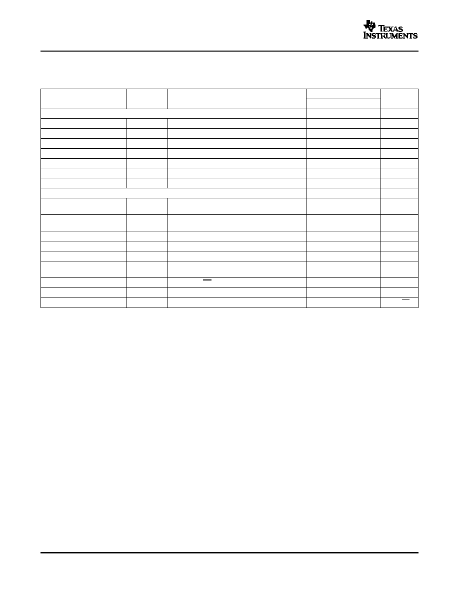
PACKAGE/ORDERING INFORMATION
(1)
MINIMUM
RELATIVE
DIFFERENTIAL
SPECIFIED
TRANSPORT
ACCURACY
NONLINEARITY
TEMPERATURE
PACKAGE-
PACKAGE
ORDERING
MEDIA,
PRODUCT
(LSB)
(LSB)
RANGE
LEAD
DESIGNATOR
NUMBER
QUANTITY
DAC8814ICDBT
Tape and Reel, 250
DAC8814C
±
1
±
1
-40
∞
C to +85
∞
C
SSOP-28
DB
DAC8814ICDBR
Tape and Reel, 2500
DAC8814IBDBT
Tape and Reel, 250
DAC8814B
±
4
±
1.5
-40
∞
C to +85
∞
C
SSOP-28
DB
DAC8814IBDBR
Tape and Reel, 2500
(1)
For the most current specifications and package information, see the Package Option Addendum located at the end of this data sheet or
refer to our web site at
www.ti.com
.
DAC8814
UNIT
V
DD
to GND
-0.3 to +8
V
V
SS
to GND
-0.3 to -7
V
V
REF
to GND
-18 to +18
V
Logic inputs and output to GND
-0.3 to + 8
V
V(I
OUT
) to GND
-0.3 to V
DD
+ 0.3
V
A
GND
X to DGND
-0.3 to +0.3
V
Input current to any pin except supplies
±
50
mA
Package power dissipation
(T
J
max - T
A
)/
JA
Thermal resistance,
JA
28-Lead shrink surface-mount (RS-28)
100
∞
C/W
Maximum junction temperature (T
J
max)
150
∞
C
Operating temperature range, Model A
-40 to +85
∞
C
Storage temperature range
-65 to + 150
∞
C
Lead temperature
RS-28 (Vapor phase 60s)
215
∞
C
RS-28 (Infrared 15s)
220
∞
C
(1)
Stresses above those listed under absolute maximum ratings may cause permanent damage to the device. This is a stress rating only;
functional operation of the device at these or any other conditions above those indicated in the operational sections of this specification
is not implied. Exposure to absolute maximum conditions for extended periods may affect device reliability.
2

www.ti.com
PRODUCT PREVIEW
ELECTRICAL CHARACTERISTICS
(1)
DAC8814
SBAS338 ≠ JANUARY 2005
V
DD
= 2.7 V to 5.0 V
±
10%; V
SS
= 0 V, I
OUT
X = Virtual GND, A
GND
X = 0 V, V
REF
A, B, C, D = 10 V, T
A
= full operating
temperature range, unless otherwise noted.
DAC8814
PARAMETER
SYMBOL
CONDITIONS
MIN
TYP
MAX
UNIT
STATIC PERFORMANCE
(2)
Resolution
16
Bits
Relative accuracy
INL
DAC8814B
±
4
LSB
INL
DAC8814C
±
1
LSB
Differential nonlinearity
DNL
DAC8814B
±
1.5
LSB
DNL
DAC8814C
±
1
LSB
Output leakage current
I
OUT
X
Data = 0000h, T
A
= 25
∞
C
10
nA
I
OUT
X
Data = 0000h, T
A
= T
A
max
20
nA
Full-scale gain error
G
FSE
Data = FFFFh
±
0.75
±
3
mV
Full-scale tempco
(3)
TCV
FS
1
ppm/
∞
C
Feedback resistor
R
FB
X
V
DD
= 5 V
5
k
REFERENCE INPUT
V
REF
X Range
V
REF
X
-15
15
V
Input resistance
R
REF
X
4
6
8
k
Input resistance match
R
REF
X
Channel-to-channel
1
%
Input capacitance
(3)
C
REF
X
5
pF
ANALOG OUTPUT
Output current
I
OUT
X
Data = FFFFh
1.25
2.5
mA
Output capacitance
(3)
C
OUT
X
Code-dependent
80
pF
LOGIC INPUTS AND OUTPUT
Input low voltage
V
IL
V
DD
= +2.7 V
0.6
V
V
IL
V
DD
= +5 V
0.8
V
Input high voltage
V
IH
V
DD
= +2.7 V
2.1
V
V
IH
V
DD
= +5 V
2.4
V
Input leakage current
I
IL
1
µA
Input capacitance
(3)
C
IL
10
pF
Logic output low voltage
V
OL
I
OL
= 1.6 mA
0.4
V
Logic output high voltage
V
OH
I
OH
= 100 µA
4
V
INTERFACE TIMING
(3)
,
(4)
Clock width high
t
CH
25
ns
Clock width low
t
CL
25
ns
CS to Clock setup
t
CSS
0
ns
Clock to CS hold
t
CSH
25
ns
Clock to SDO prop delay
t
PD
2
20
ns
Load DAC pulsewidth
t
LDAC
25
ns
Data setup
t
DS
20
ns
Data hold
t
DH
20
ns
Load setup
t
LDS
5
ns
Load hold
t
LDH
25
ns
(1)
Specifications subject to change without notice.
(2)
All static performance tests (except I
OUT
) are performed in a closed-loop system using an external precision OPA277 I-to-V converter
amplifier. The DAC8814 R
FB
terminal is tied to the amplifier output. Typical values represent average readings measured at +25
∞
C.
(3)
These parameters are specified by design and not subject to production testing.
(4)
All input control signals are specified with t
R
= t
F
= 2.5 ns (10% to 90% of 3 V) and timed from a voltage level of 1.5 V.
3
www.ti.com
PRODUCT PREVIEW
DAC8814
SBAS338 ≠ JANUARY 2005
ELECTRICAL CHARACTERISTICS (continued)
V
DD
= 2.7 V to 5.0 V
±
10%; V
SS
= 0 V, I
OUT
X = Virtual GND, A
GND
X = 0 V, V
REF
A, B, C, D = 10 V, T
A
= full operating
temperature range, unless otherwise noted.
DAC8814
PARAMETER
SYMBOL
CONDITIONS
MIN
TYP
MAX
UNIT
SUPPLY CHARACTERISTICS
Power supply range
V
DD RANGE
2.7
5.5
V
Positive supply current
I
DD
Logic inputs = 0 V
2
5
µA
I
DD
V
DD
= +4.5 V to +5.5 V
2
5
µA
I
DD
V
DD
= +2.7 V to +3.6 V
1
2.5
µA
Negative supply current
I
SS
Logic inputs = 0 V, V
SS
= -5 V
0.001
1
µA
Power dissipation
P
DISS
Logic inputs = 0 V
0.0275
mW
Power supply sensitivity
P
SS
V
DD
=
±
5%
0.006
%
AC CHARACTERISTICS
(5)
Output voltage settling time
t
s
To
±
0.1% of full-scale,
µs
0.5
Data = 0000h to FFFFh to 0000h
t
s
To
±
0.0051% of full-scale,
µs
1
Data = 0000h to FFFFh to 0000h
Reference multiplying BW
BW -3 dB V
REF
X = 100 mV
RMS
, Data = FFFF
H
, C
FB
= 15 pF
10
MHz
DAC glitch impulse
Q
V
REF
X = 10 V, Data = 0000h to 8000h to 0000h
1
nV/s
Feedthrough error
V
OUT
X/V
REF
X
Data = 0000h, V
REF
X = 100 mV
RMS
, f = 100 kHz
-70
dB
Crosstalk error
V
OUT
A/V
REF
B
Data = 0000h, V
REF
B = 100 mV
RMS
,
dB
-90
Adjacent channel, f = 100 kHz
Digital feedthrough
Q
CS = 1 and f
CLK
= 1 MHz
2
nV/s
Total harmonic distortion
THD
V
REF
= 5 V
PP
, Data = FFFFh, f = 1 kHz
-105
dB
Output spot noise voltage
e
n
f = 1 kHz, BW = 1 Hz
12
nV/
Hz
(5)
All ac characteristic tests are performed in a closed-loop system using an OPA627 I-to-V converter amplifier.
4

www.ti.com
PRODUCT PREVIEW
PIN CONFIGURATIONS
1
2
3
4
5
6
7
8
9
10
11
12
13
14
28
27
26
25
24
23
22
21
20
19
18
17
16
15
A
GND
A
I
OUT
A
V
REF
A
R
FB
A
MSB
RS
V
DD
CS
CLK
SDI
R
FB
B
V
REF
B
I
OUT
B
A
GND
B
A
GND
D
I
OUT
D
V
REF
D
R
FB
D
DGND
V
SS
A
GND
F
LDAC
SDO
NC
(1)
R
FB
C
V
REF
C
I
OUT
C
A
GND
C
DAC8814
(TOP VIEW)
NOTE (1): NC - No internal connection
DAC8814
SBAS338 ≠ JANUARY 2005
PIN DESCRIPTION
PIN
NAME
DESCRIPTION
1, 14, 15, 28
A
GND
A, A
GND
B, A
GND
C, A
GND
D
DAC A, B, C, D Analog ground.
2, 13, 16, 27
I
OUT
A, I
OUT
B, I
OUT
C, I
OUT
D
DAC A, B, C, D Current output.
DAC A, B, C, D Reference voltage input terminal. Establishes DAC A, B, C, D full-scale
3, 12, 17, 26
V
REF
A, V
REF
B, V
REF
C, V
REF
D
output voltage. Can be tied to V
DD
.
4, 11, 18, 25
R
FB
A, R
FB
B, R
FB
C, R
FB
D
Establish voltage output for DAC A, B, C, D by connecting to external amplifier output.
5
MSB
MSB Bit set during a reset pulse (RS) or at system power on if tied to ground or V
DD
.
Reset pin, active low. Input register and DAC registers are set to all zeros or half scale
6
RS
code (8000h) determined by the voltage on the MSB pin. Register data = 8000h when
MSB = 1.
7
V
DD
Positive power supply input. Specified range of operation 5 V
±
10%.
Chip-select; active low input. Disables shift register loading when high. Transfers shift
8
CS
register data to input register when CS/LDAC goes high. Does not affect LDAC operation.
9
CLK
Clock input; positive edge triggered clocks data into shift register
10
SDI
Serial data input; data loads directly into the shift register.
19
NC
Not connected; leave floating.
Serial data output; input data loads directly into shift register. Data appears at SDO, 19
20
SDO
clock pulses after input at the SDI pin.
Load DAC register strobe; level sensitive active low. Tranfers all input register data to the
21
LDAC
DAC registers. Asynchronous active low input. See Table 1 for operation.
22
A
GND
F
High current analog force ground.
23
V
SS
Negative bias power-supply input. Specified range of operation -0.3 V to -5.5 V.
24
DGND
Digital ground.
5

www.ti.com
PRODUCT PREVIEW
TYPICAL CHARACTERISTICS: V
DD
= +5 V
Channel A
Graphic
Forthcoming
Graphic
Forthcoming
Graphic
Forthcoming
Graphic
Forthcoming
DAC8814
SBAS338 ≠ JANUARY 2005
At T
A
= +25
∞
C, +V
DD
= +5 V, unless otherwise noted.
LINEARITY ERROR
DIFFERENTIAL LINEARITY ERROR
vs DIGITAL INPUT CODE
vs DIGITAL INPUT CODE
Figure 1.
Figure 2.
LINEARITY ERROR
DIFFERENTIAL LINEARITY ERROR
vs DIGITAL INPUT CODE
vs DIGITAL INPUT CODE
Figure 3.
Figure 4.
6

www.ti.com
PRODUCT PREVIEW
Graphic
Forthcoming
Graphic
Forthcoming
DAC8814
SBAS338 ≠ JANUARY 2005
TYPICAL CHARACTERISTICS: V
DD
= +5 V (continued)
At T
A
= +25
∞
C, +V
DD
= +5 V, unless otherwise noted.
LINEARITY ERROR
DIFFERENTIAL LINEARITY ERROR
vs DIGITAL INPUT CODE
vs DIGITAL INPUT CODE
Figure 5.
Figure 6.
7

www.ti.com
PRODUCT PREVIEW
Channel B
Graphic
Forthcoming
Graphic
Forthcoming
Graphic
Forthcoming
Graphic
Forthcoming
DAC8814
SBAS338 ≠ JANUARY 2005
TYPICAL CHARACTERISTICS: V
DD
= +5 V (continued)
At T
A
= +25
∞
C, +V
DD
= +5 V, unless otherwise noted.
LINEARITY ERROR
DIFFERENTIAL LINEARITY ERROR
vs DIGITAL INPUT CODE
vs DIGITAL INPUT CODE
Figure 7.
Figure 8.
LINEARITY ERROR
DIFFERENTIAL LINEARITY ERROR
vs DIGITAL INPUT CODE
vs DIGITAL INPUT CODE
Figure 9.
Figure 10.
8

www.ti.com
PRODUCT PREVIEW
Graphic
Forthcoming
Graphic
Forthcoming
DAC8814
SBAS338 ≠ JANUARY 2005
TYPICAL CHARACTERISTICS: V
DD
= +5 V (continued)
At T
A
= +25
∞
C, +V
DD
= +5 V, unless otherwise noted.
LINEARITY ERROR
DIFFERENTIAL LINEARITY ERROR
vs DIGITAL INPUT CODE
vs DIGITAL INPUT CODE
Figure 11.
Figure 12.
9

www.ti.com
PRODUCT PREVIEW
Channel C
Graphic
Forthcoming
Graphic
Forthcoming
Graphic
Forthcoming
Graphic
Forthcoming
DAC8814
SBAS338 ≠ JANUARY 2005
TYPICAL CHARACTERISTICS: V
DD
= +5 V (continued)
At T
A
= +25
∞
C, +V
DD
= +5 V, unless otherwise noted.
LINEARITY ERROR
DIFFERENTIAL LINEARITY ERROR
vs DIGITAL INPUT CODE
vs DIGITAL INPUT CODE
Figure 13.
Figure 14.
LINEARITY ERROR
DIFFERENTIAL LINEARITY ERROR
vs DIGITAL INPUT CODE
vs DIGITAL INPUT CODE
Figure 15.
Figure 16.
10

www.ti.com
PRODUCT PREVIEW
Graphic
Forthcoming
Graphic
Forthcoming
DAC8814
SBAS338 ≠ JANUARY 2005
TYPICAL CHARACTERISTICS: V
DD
= +5 V (continued)
At T
A
= +25
∞
C, +V
DD
= +5 V, unless otherwise noted.
LINEARITY ERROR
DIFFERENTIAL LINEARITY ERROR
vs DIGITAL INPUT CODE
vs DIGITAL INPUT CODE
Figure 17.
Figure 18.
11

www.ti.com
PRODUCT PREVIEW
Channel D
Graphic
Forthcoming
Graphic
Forthcoming
Graphic
Forthcoming
Graphic
Forthcoming
DAC8814
SBAS338 ≠ JANUARY 2005
TYPICAL CHARACTERISTICS: V
DD
= +5 V (continued)
At T
A
= +25
∞
C, +V
DD
= +5 V, unless otherwise noted.
LINEARITY ERROR
DIFFERENTIAL LINEARITY ERROR
vs DIGITAL INPUT CODE
vs DIGITAL INPUT CODE
Figure 19.
Figure 20.
LINEARITY ERROR
DIFFERENTIAL LINEARITY ERROR
vs DIGITAL INPUT CODE
vs DIGITAL INPUT CODE
Figure 21.
Figure 22.
12

www.ti.com
PRODUCT PREVIEW
Graphic
Forthcoming
Graphic
Forthcoming
DAC8814
SBAS338 ≠ JANUARY 2005
TYPICAL CHARACTERISTICS: V
DD
= +5 V (continued)
At T
A
= +25
∞
C, +V
DD
= +5 V, unless otherwise noted.
LINEARITY ERROR
DIFFERENTIAL LINEARITY ERROR
vs DIGITAL INPUT CODE
vs DIGITAL INPUT CODE
Figure 23.
Figure 24.
13

www.ti.com
PRODUCT PREVIEW
1.6
1.4
1.2
1.0
0.8
0.6
0.4
0.2
0
0
0.5
1.0
1.5
2.0
2.5
3.0
3.5
4.0
4.5
5.0
Logic Input Voltage (V)
V
DD
= +5.0V
V
DD
= +2.7V
Supply Current, I
D
D
(mA)
6
0
-
6
-
12
-
18
-
24
-
30
-
36
-
42
-
48
-
54
-
60
-
66
-
72
-
78
-
84
-
90
-
96
-
102
-
108
-
114
10
100
1k
10k
100k
1M
10M
100M
A
t
t
e
n
u
a
t
i
o
n
(
d
B
)
Bandwidth (Hz)
Time (0.1
µ
s/div)
O
u
t
p
u
t
V
o
l
t
a
g
e
(
5
V
/
d
i
v
)
Trigger Pulse
Voltage Output Settling
Time (0.2
µ
s/div)
O
u
t
p
u
t
V
o
l
t
a
g
e
(
5
0
m
V
/
d
i
v
)
Trigger Pulse
Code: 7FFFh to 8000h
DAC8814
SBAS338 ≠ JANUARY 2005
TYPICAL CHARACTERISTICS: V
DD
= +5 V (continued)
At T
A
= +25
∞
C, +V
DD
= +5 V, unless otherwise noted.
SUPPLY CURRENT
vs LOGIC INPUT VOLTAGE
REFERENCE MULTIPLYING BANDWIDTH
Figure 25.
Figure 26.
DAC GLITCH
DAC SETTLING TIME
Figure 27.
Figure 28.
14

www.ti.com
PRODUCT PREVIEW
TYPICAL CHARACTERISTICS: V
DD
= +2.7 V
Channel A
Graphic
Forthcoming
Graphic
Forthcoming
Graphic
Forthcoming
Graphic
Forthcoming
DAC8814
SBAS338 ≠ JANUARY 2005
At T
A
= +25
∞
C, +V
DD
= +2.7 V, unless otherwise noted.
LINEARITY ERROR
DIFFERENTIAL LINEARITY ERROR
vs DIGITAL INPUT CODE
vs DIGITAL INPUT CODE
Figure 29.
Figure 30.
LINEARITY ERROR
DIFFERENTIAL LINEARITY ERROR
vs DIGITAL INPUT CODE
vs DIGITAL INPUT CODE
Figure 31.
Figure 32.
15

www.ti.com
PRODUCT PREVIEW
Graphic
Forthcoming
Graphic
Forthcoming
DAC8814
SBAS338 ≠ JANUARY 2005
TYPICAL CHARACTERISTICS: V
DD
= +2.7 V (continued)
At T
A
= +25
∞
C, +V
DD
= +2.7 V, unless otherwise noted.
LINEARITY ERROR
DIFFERENTIAL LINEARITY ERROR
vs DIGITAL INPUT CODE
vs DIGITAL INPUT CODE
Figure 33.
Figure 34.
16

www.ti.com
PRODUCT PREVIEW
Channel B
Graphic
Forthcoming
Graphic
Forthcoming
Graphic
Forthcoming
Graphic
Forthcoming
DAC8814
SBAS338 ≠ JANUARY 2005
TYPICAL CHARACTERISTICS: V
DD
= +2.7 V (continued)
At T
A
= +25
∞
C, +V
DD
= +2.7 V, unless otherwise noted.
LINEARITY ERROR
DIFFERENTIAL LINEARITY ERROR
vs DIGITAL INPUT CODE
vs DIGITAL INPUT CODE
Figure 35.
Figure 36.
LINEARITY ERROR
DIFFERENTIAL LINEARITY ERROR
vs DIGITAL INPUT CODE
vs DIGITAL INPUT CODE
Figure 37.
Figure 38.
17

www.ti.com
PRODUCT PREVIEW
Graphic
Forthcoming
Graphic
Forthcoming
DAC8814
SBAS338 ≠ JANUARY 2005
TYPICAL CHARACTERISTICS: V
DD
= +2.7 V (continued)
At T
A
= +25
∞
C, +V
DD
= +2.7 V, unless otherwise noted.
LINEARITY ERROR
DIFFERENTIAL LINEARITY ERROR
vs DIGITAL INPUT CODE
vs DIGITAL INPUT CODE
Figure 39.
Figure 40.
18

www.ti.com
PRODUCT PREVIEW
Channel C
Graphic
Forthcoming
Graphic
Forthcoming
Graphic
Forthcoming
Graphic
Forthcoming
DAC8814
SBAS338 ≠ JANUARY 2005
TYPICAL CHARACTERISTICS: V
DD
= +2.7 V (continued)
At T
A
= +25
∞
C, +V
DD
= +2.7 V, unless otherwise noted.
LINEARITY ERROR
DIFFERENTIAL LINEARITY ERROR
vs DIGITAL INPUT CODE
vs DIGITAL INPUT CODE
Figure 41.
Figure 42.
LINEARITY ERROR
DIFFERENTIAL LINEARITY ERROR
vs DIGITAL INPUT CODE
vs DIGITAL INPUT CODE
Figure 43.
Figure 44.
19

www.ti.com
PRODUCT PREVIEW
Graphic
Forthcoming
Graphic
Forthcoming
DAC8814
SBAS338 ≠ JANUARY 2005
TYPICAL CHARACTERISTICS: V
DD
= +2.7 V (continued)
At T
A
= +25
∞
C, +V
DD
= +2.7 V, unless otherwise noted.
LINEARITY ERROR
DIFFERENTIAL LINEARITY ERROR
vs DIGITAL INPUT CODE
vs DIGITAL INPUT CODE
Figure 45.
Figure 46.
20

www.ti.com
PRODUCT PREVIEW
Channel D
Graphic
Forthcoming
Graphic
Forthcoming
Graphic
Forthcoming
Graphic
Forthcoming
DAC8814
SBAS338 ≠ JANUARY 2005
TYPICAL CHARACTERISTICS: V
DD
= +2.7 V (continued)
At T
A
= +25
∞
C, +V
DD
= +2.7 V, unless otherwise noted.
LINEARITY ERROR
DIFFERENTIAL LINEARITY ERROR
vs DIGITAL INPUT CODE
vs DIGITAL INPUT CODE
Figure 47.
Figure 48.
LINEARITY ERROR
DIFFERENTIAL LINEARITY ERROR
vs DIGITAL INPUT CODE
vs DIGITAL INPUT CODE
Figure 49.
Figure 50.
21

www.ti.com
PRODUCT PREVIEW
Graphic
Forthcoming
Graphic
Forthcoming
PARAMETER MEASUREMENT INFORMATION
SDI
CLK
CS
LDAC
SDO
t
CSS
t
ds
t
dh
t
ch
t
cl
t
csh
Input REG. LD
t
lds
t
LDAC
t
pd
t
LDH
A1
A0
D15 D14 D13
D13 D12
D11 D10
D1
D0
THEORY OF OPERATION
CIRCUIT OPERATION
D/A Converter
DAC8814
SBAS338 ≠ JANUARY 2005
TYPICAL CHARACTERISTICS: V
DD
= +2.7 V (continued)
At T
A
= +25
∞
C, +V
DD
= +2.7 V, unless otherwise noted.
LINEARITY ERROR
DIFFERENTIAL LINEARITY ERROR
vs DIGITAL INPUT CODE
vs DIGITAL INPUT CODE
Figure 51.
Figure 52.
Figure 53. DAC8814 Timing Diagram
The DAC8814 contains four, 16-bit, current-output, digital-to-analog converters (DACs) respectively. Each DAC
has its own independent multiplying reference input. The DAC8814 uses a 3-wire SPI compatible serial data
interface, with a configurable asynchronous RS pin for half-scale (MSB = 1) or zero-scale (MSB = 0) preset. In
addition, an LDAC strobe enables four channel simultaneous updates for hardware synchronized output voltage
changes.
The DAC8814 contains four current-steering R-2R ladder DACs. Figure 54 shows a typical equivalent DAC.
Each DAC contains a matching feedback resistor for use with an external I-to-V converter amplifier. The R
FB
X pin
is connected to the output of the external amplifier. The I
OUT
X terminal is connected to the inverting input of the
external amplifier. The A
GND
X pin should be Kelvin-connected to the load point in the circuit requiring the full
16-bit accuracy.
22

www.ti.com
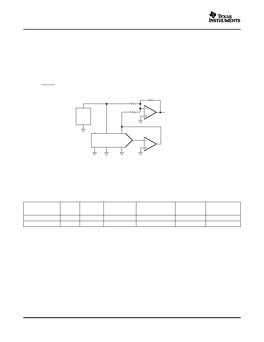
PRODUCT PREVIEW
V
OUT
+ *
V
REF
D
65536
(1)
RRR
2R
2R
2R
R
5 k
W
S2
S1
From Other DACS A
GND
V
CC
DGND
V
REF
X
V
DD
R
FB
X
I
OUT
X
A
GND
F
A
GND
X
Digital Interface Connections Omitted For Clarity.
Switches S1 and S2 are Closed, V
DD
Most be Powered.
DAC8814
SBAS338 ≠ JANUARY 2005
The DAC is designed to operate with both negative or positive reference voltages. The V
DD
power pin is only
used by the logic to drive the DAC switches on and off. Note that a matching switch is used in series with the
internal 5 k
feedback resistor. If users are attempting to measure the value of R
FB
, power must be applied to
V
DD
in order to achieve continuity. An additional V
SS
bias pin is used to guard the substrate during high
temperature applications to minimize zero-scale leakage currents that double every 10
∞
C. The DAC output
voltage is determined by V
REF
and the digital data (D) according to Equation 1:
Note that the output polarity is opposite of the V
REF
polarity for dc reference voltages.
Figure 54. Typical Equivalent DAC Channel
The DAC is also designed to accommodate ac reference input signals. The DAC8814 accommodates input
reference voltages in the range of -12 V to +12 V. The reference voltage inputs exhibit a constant nominal input
resistance of 5 k
,
±
30%. On the other hand, the DAC outputs I
OUT
A, B, C, D are code-dependent and produce
various output resistances and capacitances.
The choice of external amplifier should take into account the variation in impedance generated by the DAC8814
on the amplifiers' inverting input node. The feedback resistance, in parallel with the DAC ladder resistance,
dominates output voltage noise. For multiplying mode applications, an external feedback compensation capacitor
(C
FB
) may be needed to provide a critically damped output response for step changes in reference input
voltages.
Figure 26 shows the gain vs frequency performance at various attenuation settings using a 23 pF external
feedback capacitor connected across the I
OUT
X and R
FB
X terminals. In order to maintain good analog
performance, power supply bypassing of 0.01 µF, in parallel with 1 µF, is recommended. Under these conditions,
clean power supply with low ripple voltage capability should be used. Switching power supplies is usually not
suitable for this application due to the higher ripple voltage and P
SS
frequency-dependent characteristics. It is
best to derive the DAC8814 5-V supply from the system analog supply voltages. (Do not use the digital 5-V
supply.) See Figure 55.
23

www.ti.com
PRODUCT PREVIEW
+
+
RRR
2R
2R
2R
R
5 k
W
S2
S1
From Other DACS A
GND
V
SS
DGND
V
REF
X
V
DD
R
FB
X
I
OUT
X
A
GND
F
A
GND
X
Digital Interface Connections Omitted For Clarity.
Switches S1 and S2 are Closed, V
DD
Most be Powered.
Analog
Power
Supply
Load
15 V
2R
5 V
R
15 V
V
EE
V
CC
V
OUT
A1
DAC8814
SBAS338 ≠ JANUARY 2005
Figure 55. Recommended Kelvin-Sensed Hookup
24
www.ti.com
PRODUCT PREVIEW
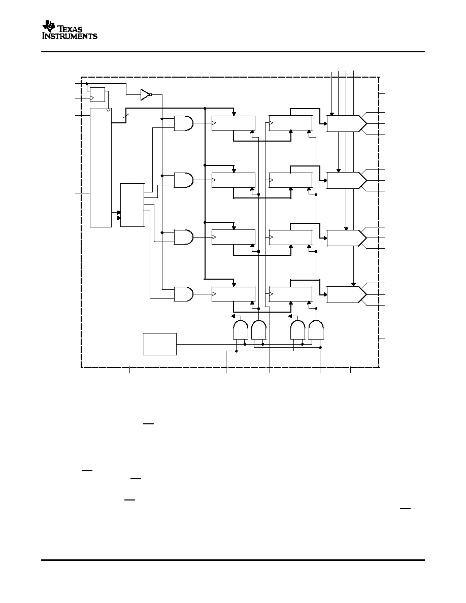
16
D0
D1
D2
D3
D4
D5
D6
D7
D8
D9
D10
D11
D12
D13
D14
D15
A0
A1
A
B
C
D
ADC
2:4
Decode
Input
Register R
Input
Register R
Input
Register R
Input
Register R
DAC A
Register R
DAC B
Register R
DAC C
Register R
DAC D
Register R
DAC A
DAC B
DAC C
DAC D
Set MSB
Set
MSB
Power-
on
Reset
DGND
MSB
LDAC
RS
V
SS
A
GND
F
A
GND
D
I
OUT
D
R
FB
D
A
GND
C
I
OUT
C
R
FB
C
A
GND
B
I
OUT
C
R
FB
B
A
GND
A
I
OUT
A
R
FB
A
V
DD
A B C D
V
REF
CS
CLK
SDI
SDO
EN
SERIAL DATA INTERFACE
DAC8814
SBAS338 ≠ JANUARY 2005
Figure 56. System Level Digital Interfacing
The DAC8814 uses a 3-wire (CS, SDI, CLK) SPI-compatible serial data interface. Serial data of the DAC8814 is
clocked into the serial input register in an 16-bit data-word format. MSB bits are loaded first. Table 2 defines the
16 data-word bits for the DAC8814.
Data is placed on the SDI pin, and clocked into the register on the positive clock edge of CLK subject to the data
setup and data hold time requirements specified in the Interface Timing Specifications. Data can only be clocked
in while the CS chip select pin is active low. For the DAC8814, only the last 16 bits clocked into the serial register
are interrogated when the CS pin returns to the logic high state.
Since most microcontrollers output serial data in 8-bit bytes, three right-justified data bytes can be written to the
DAC8814. Keeping the CS line low between the first, second, and third byte transfers results in a successful
serial register update. Similarly, two right-justified data bytes can be written to the DAC8814. Keeping the CS line
low between the first and second byte transfer will result in a successful serial register update.
25

www.ti.com
PRODUCT PREVIEW
A
B
C
D
Address
Decoder
Shift Register
EN
To Input Register
CS
CLK
SDI
SDO
19
th
/17
th
CLOCK
POWER ON RESET
ESD Protection Circuits
V
DD
5 k
W
DGND
DIGITAL
INPUTS
DAC8814
SBAS338 ≠ JANUARY 2005
Once the data is properly aligned in the shift register, the positive edge of the CS initiates the transfer of new
data to the target DAC register, determined by the decoding of address bits A1and A0. For the DAC8814,
Table 1, Table 2, Table 3 and Figure 53 define the characteristics of the software serial interface. Figure 57
shows the equivalent logic interface for the key digital control pins for the DAC8814.
Figure 57. DAC8814 Equivalent Logic Interface
Two additional pins RS and MSB provide hardware control over the preset function and DAC register loading. If
these functions are not needed, the RS pin can be tied to logic high. The asynchronous input RS pin forces all
input and DAC registers to either the zero-code state (MSB = 0), or the half-scale state (MSB = 1).
When the V
DD
power supply is turned on, an internal reset strobe forces all the Input and DAC registers to the
zero-code state or half-scale, depending on the MSB pin voltage. The V
DD
power supply should have a smooth
positive ramp without drooping in order to have consistent results, especially in the region of V
DD
= 1.5 V to
2.3 V. The V
SS
supply has no effect on the power-on reset performance. The DAC register data stays at zero or
half-scale setting until a valid serial register data load takes place.
All logic-input pins contain back-biased ESD protection zener diodes connected to ground (DGND) and V
DD
as
shown in Figure 58.
Figure 58. Equivalent ESD Protection Circuits
26

www.ti.com
PRODUCT PREVIEW
PCB LAYOUT
DAC8814
SBAS338 ≠ JANUARY 2005
In printed circuit board (PCB) layout, all analog ground A
GND
X should be tied together.
Table 1. Control Logic Truth Table
(1)
CS
CLK
LDAC
RS
MSB
SERIAL SHIFT REGISTER
INPUT REGISTER
DAC REGISTER
H
X
H
H
X
No effect
Latched
Latched
L
L
H
H
X
No effect
Latched
Latched
L
+
H
H
X
Shift register data advanced one bit
Latched
Latched
L
H
H
H
X
No effect
Latched
Latched
+
L
H
H
X
No effect
Selected DAC updated with current SR con-
Latched
tents
H
X
L
H
X
No effect
Latched
Transparent
H
X
H
H
X
No effect
Latched
Latched
H
X
+
H
X
No effect
Latched
Latched
H
X
H
L
0
No effect
Latched data = 0000h
Latched data = 0000h
X
+
H
L
H
No effect
Latched data = 8000h
Latched data = 8000h
(1)
+ = Positive logic transition; X = Do not care
Table 2. Serial Input Register Data Format, Data Loaded MSB First
(1)
B17
B0
Bit
(MSB)
B16
B15
B14
B13
B12
B11
B10
B9
B8
B7
B6
B5
B4
B3
B2
B1
(LSB)
Data
A1
A0
D15
D14
D13
D12
D11
D10
D9
D8
D7
D6
D5
D4
D3
D2
D1
D0
(1)
Only the last 18 bits of data clocked into the serial register (address + data) are inspected when the CS line positive edge returns to
logic high. At this point an internally-generated load strobe transfers the serial register data contents (bits D15-D0) to the decoded
DAC-input-register address determined by bits A1 and A0. Any extra bits clocked into the DAC8814 shift register are ignored, only the
last 18 bits clocked in are used. If double-buffered data is not needed, the LDAC pin can be tied logic low to disable the DAC registers.
Table 3. Address Decode
A1
A0
DAC DECODE
0
0
DAC A
0
1
DAC B
1
0
DAC C
1
1
DAC D
27
www.ti.com
PRODUCT PREVIEW
APPLICATION INFORMATION
V
OUT
+
D
32, 768
*
1
V
REF
(2)
10 V
V
REF
10 k
W
10 k
W
5 k
W
V
DD
V
REF
X
V
FB
X
I
OUT
X
A1
A2
A
GND
X
A
GND
FA
V
SS
One Channel
DAC8814
V
OUT
Digital Interface Connections Omitted For Clarity.
-10 V < V
OUT
< +10V
Cross-Reference
DAC8814
SBAS338 ≠ JANUARY 2005
The DAC8814, a 2-quadrant multiplying DAC, can be used to generate a unipolar output. The polarity of the
full-scale output I
OUT
is the inverse of the input reference voltage at V
REF
.
Some applications require full 4-quadrant multiplying capabilities or bipolar output swing, as shown in Figure 59.
An additional external op amp A2 is added as a summing amp. In this circuit the first and second amps (A1 and
A2) provide a gain of 2X that widens the output span to 20 V. A 4-quadrant multiplying circuit is implemented by
using a 10-V offset of the reference voltage to bias A2. According to the following circuit transfer equation (
Equation 2), input data (D) from code 0 to full scale produces output voltages of V
OUT
= -10 V to V
OUT
= 10 V.
Figure 59. Four-Quadrant Multiplying Application Circuit
The DAC8814 has an industry-standard pinout. Table 4 provides the cross-reference information.
Table 4. Cross-Reference
SPECIFIED
TEMPERATURE
PACKAGE
PACKAGE
CROSS-
PRODUCT
INL (LSB)
DNL (LSB)
RANGE
DESCRIPTION
OPTION
REFERENCE PART
DAC8814ICDB
±
1
±
1
-40
∞
C to +85
∞
C
28-Lead MicroSOIC
SSOP-28
N/A
DAC8814IBDB
±
4
±
1.5
-40
∞
C to +85
∞
C
28-Lead MicroSOIC
SSOP-28
AD5544RS
28

PACKAGING INFORMATION
Orderable Device
Status
(1)
Package
Type
Package
Drawing
Pins Package
Qty
Eco Plan
(2)
Lead/Ball Finish
MSL Peak Temp
(3)
DAC8814IBDBR
PREVIEW
SSOP
DB
28
2500
TBD
Call TI
Call TI
DAC8814IBDBT
PREVIEW
SSOP
DB
28
250
TBD
Call TI
Call TI
DAC8814ICDBR
PREVIEW
SSOP
DB
28
2500
TBD
Call TI
Call TI
DAC8814ICDBT
PREVIEW
SSOP
DB
28
250
TBD
Call TI
Call TI
(1)
The marketing status values are defined as follows:
ACTIVE: Product device recommended for new designs.
LIFEBUY: TI has announced that the device will be discontinued, and a lifetime-buy period is in effect.
NRND: Not recommended for new designs. Device is in production to support existing customers, but TI does not recommend using this part in
a new design.
PREVIEW: Device has been announced but is not in production. Samples may or may not be available.
OBSOLETE: TI has discontinued the production of the device.
(2)
Eco
Plan
-
The
planned
eco-friendly
classification:
Pb-Free
(RoHS)
or
Green
(RoHS
&
no
Sb/Br)
-
please
check
http://www.ti.com/productcontent
for the latest availability information and additional product content details.
TBD: The Pb-Free/Green conversion plan has not been defined.
Pb-Free (RoHS): TI's terms "Lead-Free" or "Pb-Free" mean semiconductor products that are compatible with the current RoHS requirements
for all 6 substances, including the requirement that lead not exceed 0.1% by weight in homogeneous materials. Where designed to be soldered
at high temperatures, TI Pb-Free products are suitable for use in specified lead-free processes.
Green (RoHS & no Sb/Br): TI defines "Green" to mean Pb-Free (RoHS compatible), and free of Bromine (Br) and Antimony (Sb) based flame
retardants (Br or Sb do not exceed 0.1% by weight in homogeneous material)
(3)
MSL, Peak Temp. -- The Moisture Sensitivity Level rating according to the JEDEC industry standard classifications, and peak solder
temperature.
Important Information and Disclaimer:The information provided on this page represents TI's knowledge and belief as of the date that it is
provided. TI bases its knowledge and belief on information provided by third parties, and makes no representation or warranty as to the
accuracy of such information. Efforts are underway to better integrate information from third parties. TI has taken and continues to take
reasonable steps to provide representative and accurate information but may not have conducted destructive testing or chemical analysis on
incoming materials and chemicals. TI and TI suppliers consider certain information to be proprietary, and thus CAS numbers and other limited
information may not be available for release.
In no event shall TI's liability arising out of such information exceed the total purchase price of the TI part(s) at issue in this document sold by TI
to Customer on an annual basis.
PACKAGE OPTION ADDENDUM
www.ti.com
30-Mar-2005
Addendum-Page 1

MECHANICAL DATA
MSSO002E ≠ JANUARY 1995 ≠ REVISED DECEMBER 2001
POST OFFICE BOX 655303
∑
DALLAS, TEXAS 75265
DB (R-PDSO-G**)
PLASTIC SMALL-OUTLINE
4040065 /E 12/01
28 PINS SHOWN
Gage Plane
8,20
7,40
0,55
0,95
0,25
38
12,90
12,30
28
10,50
24
8,50
Seating Plane
9,90
7,90
30
10,50
9,90
0,38
5,60
5,00
15
0,22
14
A
28
1
20
16
6,50
6,50
14
0,05 MIN
5,90
5,90
DIM
A MAX
A MIN
PINS **
2,00 MAX
6,90
7,50
0,65
M
0,15
0
∞
≠ 8
∞
0,10
0,09
0,25
NOTES: A. All linear dimensions are in millimeters.
B. This drawing is subject to change without notice.
C. Body dimensions do not include mold flash or protrusion not to exceed 0,15.
D. Falls within JEDEC MO-150

IMPORTANT NOTICE
Texas Instruments Incorporated and its subsidiaries (TI) reserve the right to make corrections, modifications,
enhancements, improvements, and other changes to its products and services at any time and to discontinue
any product or service without notice. Customers should obtain the latest relevant information before placing
orders and should verify that such information is current and complete. All products are sold subject to TI's terms
and conditions of sale supplied at the time of order acknowledgment.
TI warrants performance of its hardware products to the specifications applicable at the time of sale in
accordance with TI's standard warranty. Testing and other quality control techniques are used to the extent TI
deems necessary to support this warranty. Except where mandated by government requirements, testing of all
parameters of each product is not necessarily performed.
TI assumes no liability for applications assistance or customer product design. Customers are responsible for
their products and applications using TI components. To minimize the risks associated with customer products
and applications, customers should provide adequate design and operating safeguards.
TI does not warrant or represent that any license, either express or implied, is granted under any TI patent right,
copyright, mask work right, or other TI intellectual property right relating to any combination, machine, or process
in which TI products or services are used. Information published by TI regarding third-party products or services
does not constitute a license from TI to use such products or services or a warranty or endorsement thereof.
Use of such information may require a license from a third party under the patents or other intellectual property
of the third party, or a license from TI under the patents or other intellectual property of TI.
Reproduction of information in TI data books or data sheets is permissible only if reproduction is without
alteration and is accompanied by all associated warranties, conditions, limitations, and notices. Reproduction
of this information with alteration is an unfair and deceptive business practice. TI is not responsible or liable for
such altered documentation.
Resale of TI products or services with statements different from or beyond the parameters stated by TI for that
product or service voids all express and any implied warranties for the associated TI product or service and
is an unfair and deceptive business practice. TI is not responsible or liable for any such statements.
Following are URLs where you can obtain information on other Texas Instruments products and application
solutions:
Products
Applications
Amplifiers
amplifier.ti.com
Audio
www.ti.com/audio
Data Converters
dataconverter.ti.com
Automotive
www.ti.com/automotive
DSP
dsp.ti.com
Broadband
www.ti.com/broadband
Interface
interface.ti.com
Digital Control
www.ti.com/digitalcontrol
Logic
logic.ti.com
Military
www.ti.com/military
Power Mgmt
power.ti.com
Optical Networking
www.ti.com/opticalnetwork
Microcontrollers
microcontroller.ti.com
Security
www.ti.com/security
Telephony
www.ti.com/telephony
Video & Imaging
www.ti.com/video
Wireless
www.ti.com/wireless
Mailing Address:
Texas Instruments
Post Office Box 655303 Dallas, Texas 75265
Copyright
2005, Texas Instruments Incorporated