www.ti.com
FEATURES
DESCRIPTION
APPLICATIONS
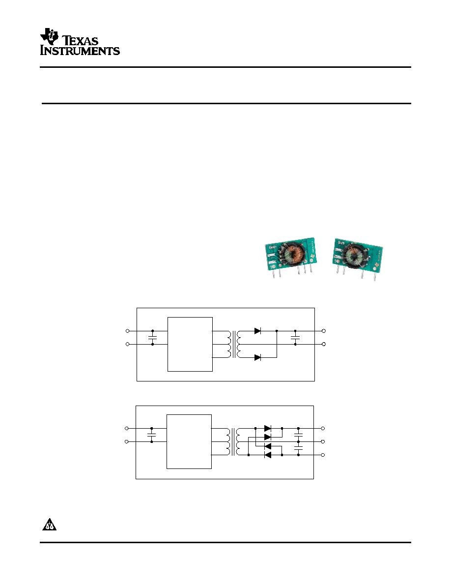
Power
Controller
+V
O
-
V
O
+V
I
-
V
I
Power
Controller
+V
O
COM
+V
I
-
V
I
-
V
O
DCH01 Series
SBVS073C ≠ MAY 2006 ≠ REVISED AUGUST 2006
MINIATURE, 1W, 3kV ISOLATED
UNREGULATED DC/DC CONVERTERS
∑
Up To 78% Efficiency
The DCH01 series is a family of miniature, 1W, 3kV
isolated DC/DC converters. Featured in an industry
∑
3kVDC Isolation
standard SIP-7 footprint, the DCH01 series requires
∑
UL60950 Certified Product (pending)
minimal external components, reducing board space.
∑
Industry Standard Footprint
The DCH01 series provides both single and dual
∑
JEDEC SIP-7 Package
split-supply outputs.
The use of a highly integrated package design
results in highly reliable products with high power
∑
Point-of-Use Power Conversion
densities. High performance and small size makes
the DCH01 suitable for a wide range of applications
∑
Ground Loop Elimination
including signal chain applications and ground loop
∑
Data Acquisition
elimination.
∑
Industrial Control and Instrumentation
∑
Test Equipment
Single Output Block Diagram
Dual Output Block Diagram
Please be aware that an important notice concerning availability, standard warranty, and use in critical applications of Texas
Instruments semiconductor products and disclaimers thereto appears at the end of this data sheet.
All trademarks are the property of their respective owners.
PRODUCTION DATA information is current as of publication date.
Copyright © 2006, Texas Instruments Incorporated
Products conform to specifications per the terms of the Texas
Instruments standard warranty. Production processing does not
necessarily include testing of all parameters.
www.ti.com
ORDERING INFORMATION
ABSOLUTE MAXIMUM RATINGS
DCH01 Series
SBVS073C ≠ MAY 2006 ≠ REVISED AUGUST 2006
This integrated circuit can be damaged by ESD. Texas Instruments recommends that all integrated circuits be handled with
appropriate precautions. Failure to observe proper handling and installation procedures can cause damage.
ESD damage can range from subtle performance degradation to complete device failure. Precision integrated circuits may be
more susceptible to damage because very small parametric changes could cause the device not to meet its published
specifications.
For the most current package and ordering information, see the Package Option Addendum at the end of this
data sheet, or see the TI website at www.ti.com.
Part Numbering Scheme
INPUT
OUTPUT
PIN
TRANSPORT
PRODUCT LINE
POWER
VOLTAGE
VOLTAGE
SINGLE/DUAL
PACKAGE
CONFIG
MEDIA
DCH
01
05
05
S
N
7
H = 3kV, unregulated output
01 = 1W
05 = 5V
05 = 5V
S = Single
N = SIP Thru-hole
7 = SIP-7
Blank = Tray
12 =12V
D = Dual
T = Tape & Reel
15 = 15V
DCH01 Products
OUTPUT
OUTPUT
ISOLATION
INPUT VOLTAGE
VOLTAGE
CURRENT
OUTPUT POWER
VOLTAGE
MODEL
(V)
(V)
(mA)
(W)
(kVDC)
PACKAGE-LEAD
DCH010505S
5
±
10%
5
200
1
3
SIP-7
DCH010512S
5
±
10%
12
83
1
3
SIP-7
DCH010515S
5
±
10%
15
67
1
3
SIP-7
DCH010505D
5
±
10%
±
5
±
100
1
3
SIP-7
DCH010512D
5
±
10%
±
12
±
42
1
3
SIP-7
DCH010515D
5
±
10%
±
15
±
33
1
3
SIP-7
over operating free-air temperature range (unless otherwise noted)
(1)
DCH01 SERIES
UNIT
Input Voltage
5V input models
7
V
Storage temperature range
≠40 to +125
∞
C
(1)
Stresses beyond those listed under Absolute Maximum Ratings may cause permanent damage to the device. These are stress ratings
only, and functional operation of the device at these or any other conditions beyond those indicated is not implied. Exposure to absolute
maximum rated conditions for extended periods may affect device reliability.
2
Submit Documentation Feedback
www.ti.com
ELECTRICAL CHARACTERISTICS
ELECTRICAL CHARACTERISTICS PER DEVICE
DCH01 Series
SBVS073C ≠ MAY 2006 ≠ REVISED AUGUST 2006
At T
A
= +25
∞
C, V
I
= 5V unless otherwise noted.
PARAMETER
TEST CONDITIONS
MIN
TYP
MAX
UNIT
OUTPUT
Power
100% full load
1
W
INPUT
Voltage range on V
I
≠10
10
%
ISOLATION
60s test, UL60950
(1)
3
kVDC
Voltage
100% tested for 1s
3.5
kVDC
LINE
Regulation
1% change in V
I
1
%
SWITCHING
Switching frequency (f
SW
)
70
kHz
RELIABILITY
Single Output
18
Calculated
Per Telcordia SR-332; 50% stress; T
A
= +40∞C
FITS
Dual Output
22
TEMPERATURE RANGE
Operating
≠40
+85
∞
C
(1)
During UL60950 recognition tests only.
At T
A
= +25
∞
C, V
I
= 5V unless otherwise noted.
NO LOAD
INPUT
OUTPUT
LOAD
OUTPUT
INPUT
BARRIER
VOLTAGE
VOLTAGE
REGULATION
RIPPLE
(1)
CURRENT
EFFICIENCY
CAPACITANCE
(V)
(V)
(%)
(mV
PP
)
(mA)
(%)
(pF)
V
I
V
NOM
I
Q
C
ISO
10% TO 100%
NOMINAL
100% LOAD
(2)
LOAD
(3)
100% LOAD
(2)
0% LOAD
100% LOAD
(2)
PRODUCT
TYP
TYP
TYP
TYP
TYP
TYP
TYP
DCH010505S
5
5.1
10
35
60
72
3
DCH010505D
5
±
5.2
9
20
60
72
3
DCH010512S
5
12.4
6
18
65
74
4
DCH010512D
5
±
12.5
5
19
65
75
4
DCH010515S
5
15.2
6
31
65
75
3
DCH010515D
5
±
15.3
5
22
65
76
3
(1)
20MHz bandwidth.
(2)
100% load current = 1W/V
NOM
typ.
(3)
Load Regulation = (V
O
at 10% load - V
O
at 100% load) / V
O
at 100% load.
3
Submit Documentation Feedback
www.ti.com
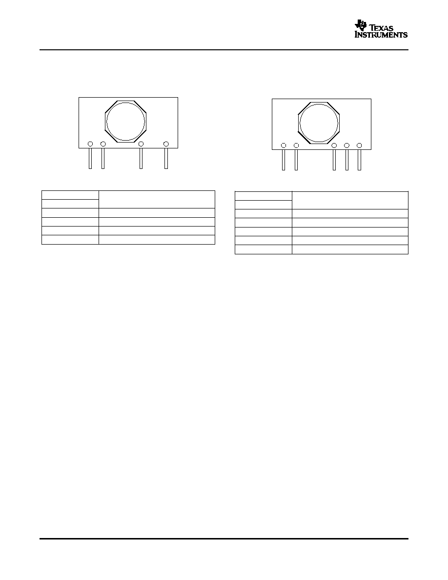
DEVICE INFORMATION
1
2
5
7
DCH01
1
2
5
6
7
DCH01
DCH01 Series
SBVS073C ≠ MAY 2006 ≠ REVISED AUGUST 2006
EDJ PACKAGE
EDJ PACKAGE
SIP-7 (Single)
SIP-7 (Dual)
(Top View)
(Top View)
Pin Description (Single)
Pin Descriptions (Dual)
TERMINAL
TERMINAL
NAME
NO.
DESCRIPTION
NAME
NO.
DESCRIPTION
+V
I
1
Voltage input
+V
I
1
Voltage input
≠V
I
2
Input side common
≠V
I
2
Input side common
≠V
O
5
≠Voltage out
≠V
O
5
≠Voltage out
+V
O
7
+Voltage out
COM
6
Output side common
+V
O
7
+Voltage out
4
Submit Documentation Feedback
www.ti.com
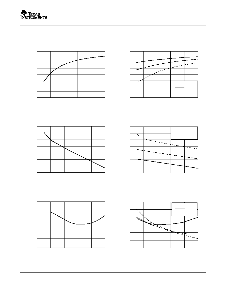
TYPICAL CHARACTERISTICS
Efficiency(%)
I , Load Current (mA)
O
80
70
60
50
40
30
20
10
0
0
40
200
80
120
160
Efficiency(%)
Output 1 Load Current (mA)
80
70
60
50
40
30
20
10
0
0
20
100
40
60
80
Output 2 Load Current
100mA
50mA
10mA
V
,OutputV
oltage(V)
O
I , Load Current (mA)
O
5.7
5.6
5.5
5.4
5.3
5.2
5.1
5.0
0
40
200
80
120
160
V
,OutputV
oltage(V)
O
Output 1 Load Current (mA)
5.8
5.7
5.6
5.5
5.4
5.3
5.2
5.1
0
20
100
40
60
80
Output 2 Load Current
100mA
50mA
10mA
OutputV
oltageRipple(mV
)
PP
I , Load Current (mA)
O
50
40
30
20
10
0
0
40
200
80
120
160
OutputV
oltageRipple(mV
)
PP
Output 1 Load Current (mA)
30
25
20
15
10
5
0
0
20
100
40
60
80
Output 2 Load Current
100mA
50mA
10mA
DCH01 Series
SBVS073C ≠ MAY 2006 ≠ REVISED AUGUST 2006
At T
A
= +25
∞
C, and V
IN
= 5V unless otherwise noted.
DCH010505S
DCH010505D
EFFICIENCY
EFFICIENCY
Figure 1.
Figure 2.
DCH010505S
DCH010505D
LOAD REGULATION
LOAD REGULATION
Figure 3.
Figure 4.
DCH010505S
DCH010505D
RIPPLE VOLTAGE
RIPPLE VOLTAGE
Figure 5.
Figure 6.
5
Submit Documentation Feedback
www.ti.com
Efficiency(%)
I , Load Current (mA)
O
80
70
60
50
40
30
20
10
0
0
15
90
30
45
60
75
Efficiency(%)
Output 1 Load Current (mA)
80
70
60
50
40
30
20
10
0
0
10
15
5
45
20
25
30
35
40
Output 2 Load Current
42mA
21mA
4mA
V
,OutputV
oltage(V)
O
I , Load Current (mA)
O
13.2
13.0
12.8
12.6
12.4
12.2
0
15
90
30
45
60
75
V
,OutputV
oltage(V)
O
Output 1 Load Current (mA)
13.2
13.1
13.0
12.9
12.8
12.7
12.6
12.5
12.4
12.3
0
10
15
5
45
20
25
30
35
40
Output 2 Load Current
42mA
21mA
4mA
OutputV
oltageRipple(mV
)
PP
I , Load Current (mA)
O
50
40
30
20
10
0
15
90
30
45
60
75
OutputV
oltageRipple(mV
)
PP
Output 1 Load Current (mA)
20
16
12
8
4
0
0
10
15
5
45
20
25
30
35
40
Output 2 Load Current
42mA
21mA
4mA
DCH01 Series
SBVS073C ≠ MAY 2006 ≠ REVISED AUGUST 2006
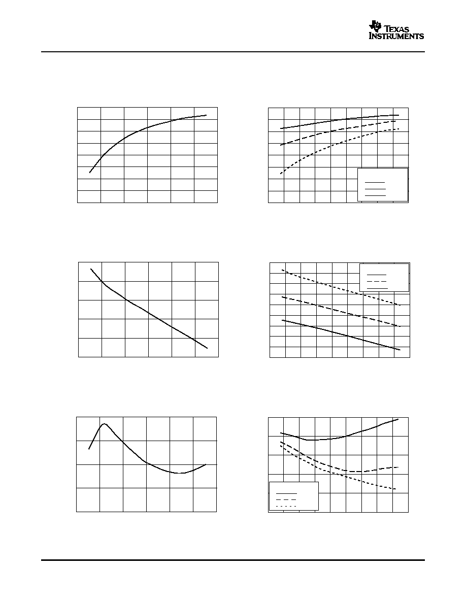
TYPICAL CHARACTERISTICS (continued)
At T
A
= +25
∞
C, and V
IN
= 5V unless otherwise noted.
DCH010512S
DCH010512D
EFFICIENCY
EFFICIENCY
Figure 7.
Figure 8.
DCH010512S
DCH010512D
LOAD REGULATION
LOAD REGULATION
Figure 9.
Figure 10.
DCH010512S
DCH010512D
RIPPLE VOLTAGE
RIPPLE VOLTAGE
Figure 11.
Figure 12.
6
Submit Documentation Feedback
www.ti.com
Efficiency(%)
I , Load Current (mA)
O
80
70
60
50
40
30
20
10
0
0
15
75
30
45
60
Efficiency(%)
Output 1 Load Current (mA)
80
70
60
50
40
30
20
10
0
0
20
30
35
15
10
5
25
Output 2 Load Current
33mA
17mA
3mA
V
,OutputV
oltage(V)
O
I , Load Current (mA)
O
16.5
16.2
15.9
15.6
15.3
15.0
0
15
75
30
45
60
V
,OutputV
oltage(V)
O
Output 1 Load Current (mA)
16.1
16.0
15.9
15.8
15.7
15.6
15.5
15.4
15.3
15.2
15.1
0
20
30
35
15
10
5
25
Output 2 Load Current
33mA
17mA
3mA
OutputV
oltageRipple(mV
)
PP
I , Load Current (mA)
O
50
45
40
35
30
25
20
0
15
75
30
45
60
OutputV
oltageRipple(mV
)
PP
Output 1 Load Current (mA)
25
20
15
10
5
0
20
30
35
15
10
5
25
Output 2 Load Current
33mA
17mA
3mA
DCH01 Series
SBVS073C ≠ MAY 2006 ≠ REVISED AUGUST 2006
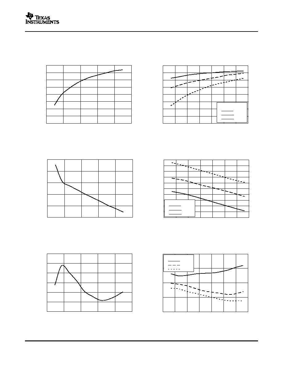
TYPICAL CHARACTERISTICS (continued)
At T
A
= +25
∞
C, and V
IN
= 5V unless otherwise noted.
DCH010515S
DCH010515D
EFFICIENCY
EFFICIENCY
Figure 13.
Figure 14.
DCH010515S
DCH010515D
LOAD REGULATION
LOAD REGULATION
Figure 15.
Figure 16.
DCH010515S
DCH010515D
RIPPLE VOLTAGE
RIPPLE VOLTAGE
Figure 17.
Figure 18.
7
Submit Documentation Feedback
www.ti.com
AmbientT
emperature(
C)
∞
Load Current (%)
90
80
70
60
50
40
30
20
0
20
100
40
60
80
Natural Convection
DCH01 Series
SBVS073C ≠ MAY 2006 ≠ REVISED AUGUST 2006
TYPICAL CHARACTERISTICS (continued)
At T
A
= +25
∞
C, and V
IN
= 5V unless otherwise noted.
SAFE OPERATING AREA
(All DCH0105 Products)
Figure 19.
8
Submit Documentation Feedback
PACKAGING INFORMATION
Orderable Device
Status
(1)
Package
Type
Package
Drawing
Pins Package
Qty
Eco Plan
(2)
Lead/Ball Finish
MSL Peak Temp
(3)
DCH010505DN7
ACTIVE
SIP MOD
ULE
EDJ
5
70
Pb-Free
(RoHS)
Call TI
N / A for Pkg Type
DCH010505SN7
ACTIVE
SIP MOD
ULE
EDJ
4
70
Pb-Free
(RoHS)
Call TI
N / A for Pkg Type
DCH010512DN7
ACTIVE
SIP MOD
ULE
EDJ
5
70
Pb-Free
(RoHS)
Call TI
N / A for Pkg Type
DCH010512SN7
ACTIVE
SIP MOD
ULE
EDJ
4
70
Pb-Free
(RoHS)
Call TI
N / A for Pkg Type
DCH010515DN7
ACTIVE
SIP MOD
ULE
EDJ
5
70
Pb-Free
(RoHS)
Call TI
N / A for Pkg Type
DCH010515SN7
ACTIVE
SIP MOD
ULE
EDJ
4
70
Pb-Free
(RoHS)
Call TI
N / A for Pkg Type
(1)
The marketing status values are defined as follows:
ACTIVE: Product device recommended for new designs.
LIFEBUY: TI has announced that the device will be discontinued, and a lifetime-buy period is in effect.
NRND: Not recommended for new designs. Device is in production to support existing customers, but TI does not recommend using this part in
a new design.
PREVIEW: Device has been announced but is not in production. Samples may or may not be available.
OBSOLETE: TI has discontinued the production of the device.
(2)
Eco Plan - The planned eco-friendly classification: Pb-Free (RoHS), Pb-Free (RoHS Exempt), or Green (RoHS & no Sb/Br) - please check
http://www.ti.com/productcontent
for the latest availability information and additional product content details.
TBD: The Pb-Free/Green conversion plan has not been defined.
Pb-Free (RoHS): TI's terms "Lead-Free" or "Pb-Free" mean semiconductor products that are compatible with the current RoHS requirements
for all 6 substances, including the requirement that lead not exceed 0.1% by weight in homogeneous materials. Where designed to be soldered
at high temperatures, TI Pb-Free products are suitable for use in specified lead-free processes.
Pb-Free (RoHS Exempt): This component has a RoHS exemption for either 1) lead-based flip-chip solder bumps used between the die and
package, or 2) lead-based die adhesive used between the die and leadframe. The component is otherwise considered Pb-Free (RoHS
compatible) as defined above.
Green (RoHS & no Sb/Br): TI defines "Green" to mean Pb-Free (RoHS compatible), and free of Bromine (Br) and Antimony (Sb) based flame
retardants (Br or Sb do not exceed 0.1% by weight in homogeneous material)
(3)
MSL, Peak Temp. -- The Moisture Sensitivity Level rating according to the JEDEC industry standard classifications, and peak solder
temperature.
Important Information and Disclaimer:The information provided on this page represents TI's knowledge and belief as of the date that it is
provided. TI bases its knowledge and belief on information provided by third parties, and makes no representation or warranty as to the
accuracy of such information. Efforts are underway to better integrate information from third parties. TI has taken and continues to take
reasonable steps to provide representative and accurate information but may not have conducted destructive testing or chemical analysis on
incoming materials and chemicals. TI and TI suppliers consider certain information to be proprietary, and thus CAS numbers and other limited
information may not be available for release.
In no event shall TI's liability arising out of such information exceed the total purchase price of the TI part(s) at issue in this document sold by TI
to Customer on an annual basis.
PACKAGE OPTION ADDENDUM
www.ti.com
10-Aug-2006
Addendum-Page 1

IMPORTANT NOTICE
Texas Instruments Incorporated and its subsidiaries (TI) reserve the right to make corrections, modifications,
enhancements, improvements, and other changes to its products and services at any time and to discontinue
any product or service without notice. Customers should obtain the latest relevant information before placing
orders and should verify that such information is current and complete. All products are sold subject to TI's terms
and conditions of sale supplied at the time of order acknowledgment.
TI warrants performance of its hardware products to the specifications applicable at the time of sale in
accordance with TI's standard warranty. Testing and other quality control techniques are used to the extent TI
deems necessary to support this warranty. Except where mandated by government requirements, testing of all
parameters of each product is not necessarily performed.
TI assumes no liability for applications assistance or customer product design. Customers are responsible for
their products and applications using TI components. To minimize the risks associated with customer products
and applications, customers should provide adequate design and operating safeguards.
TI does not warrant or represent that any license, either express or implied, is granted under any TI patent right,
copyright, mask work right, or other TI intellectual property right relating to any combination, machine, or process
in which TI products or services are used. Information published by TI regarding third-party products or services
does not constitute a license from TI to use such products or services or a warranty or endorsement thereof.
Use of such information may require a license from a third party under the patents or other intellectual property
of the third party, or a license from TI under the patents or other intellectual property of TI.
Reproduction of information in TI data books or data sheets is permissible only if reproduction is without
alteration and is accompanied by all associated warranties, conditions, limitations, and notices. Reproduction
of this information with alteration is an unfair and deceptive business practice. TI is not responsible or liable for
such altered documentation.
Resale of TI products or services with statements different from or beyond the parameters stated by TI for that
product or service voids all express and any implied warranties for the associated TI product or service and
is an unfair and deceptive business practice. TI is not responsible or liable for any such statements.
Following are URLs where you can obtain information on other Texas Instruments products and application
solutions:
Products
Applications
Amplifiers
amplifier.ti.com
Audio
www.ti.com/audio
Data Converters
dataconverter.ti.com
Automotive
www.ti.com/automotive
DSP
dsp.ti.com
Broadband
www.ti.com/broadband
Interface
interface.ti.com
Digital Control
www.ti.com/digitalcontrol
Logic
logic.ti.com
Military
www.ti.com/military
Power Mgmt
power.ti.com
Optical Networking
www.ti.com/opticalnetwork
Microcontrollers
microcontroller.ti.com
Security
www.ti.com/security
Low Power Wireless www.ti.com/lpw
Telephony
www.ti.com/telephony
Video & Imaging
www.ti.com/video
Wireless
www.ti.com/wireless
Mailing Address:
Texas Instruments
Post Office Box 655303 Dallas, Texas 75265
Copyright
2006, Texas Instruments Incorporated