
Miniature, 1W Isolated
UNREGULATED DC/DC CONVERTERS
Copyright © 2000, Texas Instruments, Incorporated
SBVS012A
Printed in U.S.A. December, 2000
DCP01B
Series
FEATURES
q
UP TO 85% EFFICIENCY
q
THERMAL PROTECTION
q
DEVICE-TO-DEVICE SYNCHRONIZATION
q
SHORT CIRCUIT PROTECTION
q
EN55022 CLASS B EMC PERFORMANCE
q
UL1950 RECOGNIZED COMPONENT
q
JEDEC PDIP-14 AND GULL-WING PACKAGES
DESCRIPTION
The DCP01B series is a family of 1W, unregulated, isolated
DC/DC converters. Requiring a minimum of external com-
ponents and including on-chip device protection, the DCP01B
series provides extra features such as output disable and
synchronization of switching frequencies.
APPLICATIONS
q
POINT-OF-USE POWER CONVERSION
q
GROUND LOOP ELIMINATION
q
DATA ACQUISITION
q
INDUSTRIAL CONTROL AND
INSTRUMENTATION
q
TEST EQUIPMENT
I
BIAS
Power
Stage
V
OUT
˜
2
Reset
800kHz
Oscillator
Watch-dog/
start-up
PSU
Thermal
Shutdown
SYNC
OUT
SYNC
IN
V
S
0V
Power Controller IC
0V
DCP0
1
DCP01
www.ti.com
The use of a highly integrated package design
results in highly reliable products with a power
density of 40W/in
3
(2.4W/cm
3
). This combination
of features and small size makes the DCP01B
suitable for a wide range of applications.

DCP01B
2
SBVS012A
Basic Model Number: 1W Product
Voltage Input:
5V In
Voltage Output:
5V Out
Dual Output:
Model Revision:
Package Code:
P = PDIP-14
P-U = PDIP-14 Gull-Wing
05
ELECTROSTATIC
DISCHARGE SENSITIVITY
This integrated circuit can be damaged by ESD. Burr-Brown
recommends that all integrated circuits be handled with
appropriate precautions. Failure to observe proper handling
and installation procedures can cause damage.
ESD damage can range from subtle performance degrada-
tion to complete device failure. Precision integrated circuits
may be more susceptible to damage because very small
parametric changes could cause the device not to meet its
published specifications.
Input Voltage:
5V Input Models .................................................................................. 7V
15V Input Models .............................................................................. 18V
24V Input Models .............................................................................. 29V
Storage Temperature ...................................................... ≠40
∞
C to +125
∞
C
Lead Temperature (soldering, 10s) ................................................. 270
∞
C
ABSOLUTE MAXIMUM RATINGS
ORDERING INFORMATION
05
(
)
( D )
INPUT
OUTPUT
LOAD
NO LOAD
BARRIER
VOLTAGE (V)
VOLTAGE (V)
REGULATION (%)
CURRENT (mA)
EFFICIENCY (%)
CAPACITANCE (pF)
V
S
V
NOM
I
Q
C
ISO
75% LOAD
(2)
10% TO 100% LOAD
(3)
0% LOAD
100% LOAD
V
ISO
= 750V
RMS
PRODUCT
MIN
TYP
MAX
MIN
TYP
MAX
TYP
MAX
TYP
TYP
TYP
DCP010505B
4.5
5
5.5
4.75
5
5.25
19
31
20
80
3.6
DCP010505DB
4.5
5
5.5
±
4.25
±
5
±
5.75
18
32
22
81
3.8
DCP010512B
4.5
5
5.5
11.4
12
12.6
21
38
29
85
5.1
DCP010512DB
4.5
5
5.5
±
11.4
±
12
±
12.6
19
37
40
82
4.0
DCP010515B
4.5
5
5.5
14.25
15
15.75
26
42
34
82
3.8
DCP010515DB
4.5
5
5.5
±
14.25
±
15
±
15.75
19
41
42
85
4.7
DCP011512DB
13.5
15
16.5
±
11.4
±
12
±
12.6
11
39
19
78
2.5
DCP011515DB
13.5
15
16.5
±
14.25
±
15
±
15.75
12
39
20
80
2.5
DCP012405B
21.6
24
26.4
4.75
5
5.25
13
23
14
77
2.5
DCP012415DB
21.6
24
26.4
±
14.25
±
15
±
15.75
10
35
17
76
3.8
NOTES: (1) During UL1950 recognition tests only. (2) 100% Load Current = 1W/V
NOM
TYP. (3) Load regulation = (V
OUT
at 10% Load ≠ V
OUT
at 100% Load)/V
OUT
at 75% Load.
SPECIFICATIONS
At T
A
= +25
∞
C, unless otherwise specified.
DCP01B SERIES
PARAMETER
CONDITIONS
MIN
TYP
MAX
UNITS
OUTPUT
Power
100% Full Load
0.97
W
Ripple
O/P Capacitor = 1
µ
F, 50% Load
20
mVp-p
Voltage vs Temp
Room to Cold
0.046
%/
∞
C
Room to Hot
0.016
%/
∞
C
INPUT
Voltage Range on V
S
≠10
10
%
ISOLATION
Voltage
1s Flash Test
1
kVrms
60s Test, UL1950
(1)
1
kVrms
LINE
Regulation
1
%/1% of V
S
SWITCHING/SYNCHRONIZATION
Oscillator Frequency (f
OSC
)
Switching Frequency = f
OSC
/2
800
kHz
Sync Input Low
0
0.4
V
Sync Input Current
V
SYNC
= +2V
75
µ
A
Disable Time
2
µ
s
Capacitance Loading on SYNC
IN
Pin
External
3
pF
RELIABILITY
Demonstrated
T
A
= +55
∞
C
75
FITS
THERMAL SHUTDOWN
IC Temperature at Shutdown
150
∞
C
Shutdown Current
3
mA
TEMPERATURE RANGE
Operating
≠40
+100
∞
C
DCP01
( B )
DCP01B
3
SBVS012A
PACKAGE
SPECIFIED
DRAWING
TEMPERATURE
PACKAGE
ORDERING
TRANSPORT
PRODUCT
PACKAGE
NUMBER
RANGE
MARKING
NUMBER
(1)
MEDIA
Single
DCP010505BP
DIP-14
010-1
≠40
∞
C to +100
∞
C
DCP010505BP
DCP010505BP
Rails
DCP010505BP-U
DIP-14 Gull-Wing
010-2
≠40
∞
C to +100
∞
C
DCP010505BP-U
DCP010505BP-U/700
Tape and Reel
DCP010512BP
DIP-14
010-1
≠40
∞
C to +100
∞
C
DCP010512BP
DCP010512BP
Rails
DCP010512BP-U
DIP-14 Gull-Wing
010-2
≠40
∞
C to +100
∞
C
DCP010512BP-U
DCP010512BP-U/700
Tape and Reel
DCP010515BP
DIP-14
010-1
≠40
∞
C to +100
∞
C
DCP010515BP
DCP010515BP
Rails
DCP010515BP-U
DIP-14 Gull-Wing
010-2
≠40
∞
C to +100
∞
C
DCP010515BP-U
DCP010515BP-U/700
Tape and Reel
DCP012405BP
DIP-14
010-1
≠40
∞
C to +100
∞
C
DCP012405BP
DCP012405BP
Rails
DCP012405BP-U
DIP-14 Gull-Wing
010-2
≠40
∞
C to +100
∞
C
DCP012405BP-U
DCP012405BP-U/700
Tape and Reel
Dual
DCP010505DBP
DIP-14
010-1
≠40
∞
C to +100
∞
C
DCP010505DBP
DCP010505DBP
Rails
DCP010505DBP-U
DIP-14 Gull-Wing
010-2
≠40
∞
C to +100
∞
C
DCP010505DBP-U
DCP010505DBP-U/ 700
Tape and Reel
DCP010512DBP
DIP-14
010-1
≠40
∞
C to +100
∞
C
DCP010512DBP
DCP010512DBP
Rails
DCP010512DBP-U
DIP-14 Gull-Wing
010-2
≠40
∞
C to +100
∞
C
DCP010512DBP-U
DCP010512DBP-U/ 700
Tape and Reel
DCP010515DBP
DIP-14
010-1
≠40
∞
C to +100
∞
C
DCP010515DBP
DCP010515DBP
Rails
DCP010515DBP-U
DIP-14 Gull-Wing
010-2
≠40
∞
C to +100
∞
C
DCP010515DBP-U
DCP010515DBP-U/ 700
Tape and Reel
Dual
DCP011512DBP
DIP-14
010-1
≠40
∞
C to +100
∞
C
DCP011512DBP
DCP011512DBP
Rails
DCP011512DBP-U
DIP-14 Gull-Wing
010-2
≠40
∞
C to +100
∞
C
DCP011512DBP-U
DCP011512DBP-U/700
Tape and Reel
DCP011515DBP
DIP-14
010-1
≠40
∞
C to +100
∞
C
DCP011515DBP
DCP011515DBP
Rails
DCP011515DBP-U
DIP-14 Gull-Wing
010-2
≠40
∞
C to +100
∞
C
DCP011515DBP-U
DCP011515DBP-U/ 700
Tape and Reel
DCP012415DBP
DIP-14
010-1
≠40
∞
C to +100
∞
C
DCP012415DBP
DCP012415DBP
Rails
DCP012415DBP-U
DIP-14 Gull-Wing
010-2
≠40
∞
C to +100
∞
C
DCP012415DBP-U
DCP012415DBP-U/700
Tape and Reel
NOTE: (1) Models with a slash (/) are available only in Tape and Reel in the quantities indicated (e.g., /700 indicates 700 devices per reel). Ordering 700 pieces
of "DCP010505BP-U/700" will get a single 700-piece Tape and Reel.
PACKAGE/ORDERING INFORMATION
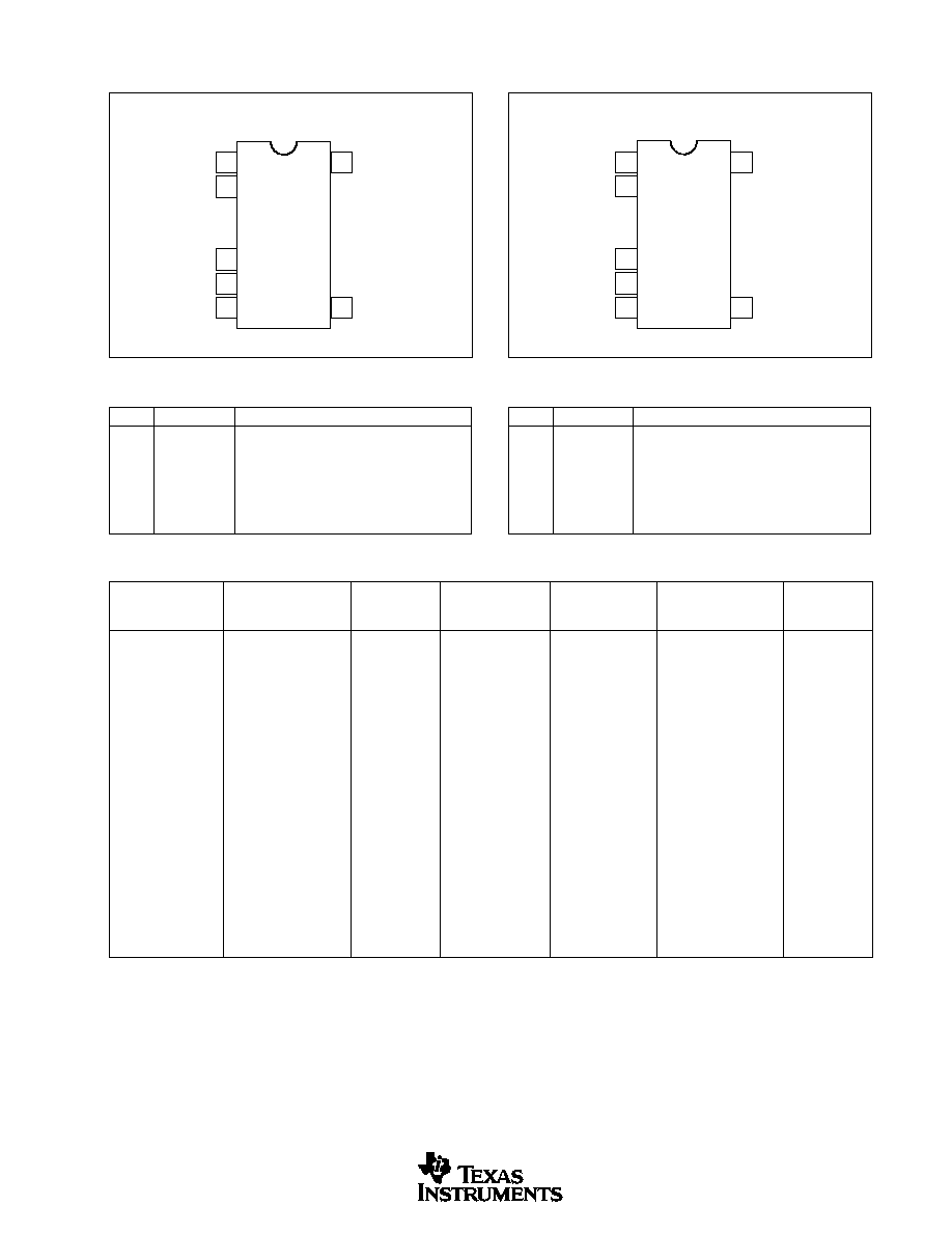
Top View
DIP
PIN CONFIGURATION (Single-DIP and Gull-Wing)
Top View
DIP
PIN CONFIGURATION (Dual-DIP and Gull-Wing)
PIN DEFINITION (Single-DIP)
PIN #
PIN NAME
DESCRIPTION
1
V
S
Voltage Input
2
0V
Input Side Common
5
0V
Output Side Common
6
+V
OUT
+Voltage Out
7
NC
Not Connected
8
SYNC
OUT
Unrectified Transformer Output
14
SYNC
IN
Synchronization Pin
PIN DEFINITION (Dual-DIP)
PIN #
PIN NAME
DESCRIPTION
1
V
S
Voltage Input
2
0V
Input Side Common
5
0V
Output Side Common
6
+V
OUT
+Voltage Out
7
≠V
OUT
≠Voltage Out
8
SYNC
OUT
Unrectified Transformer Output
14
SYNC
IN
Synchronization Pin
DCP01DB
1
2
5
6
7
14
8
V
S
0V
0V
+V
OUT
≠V
OUT
SYNC
IN
SYNC
OUT
DCP01B
1
2
5
6
7
14
8
V
S
0V
0V
+V
OUT
NC
SYNC
IN
SYNC
OUT
DCP01B
4
SBVS012A
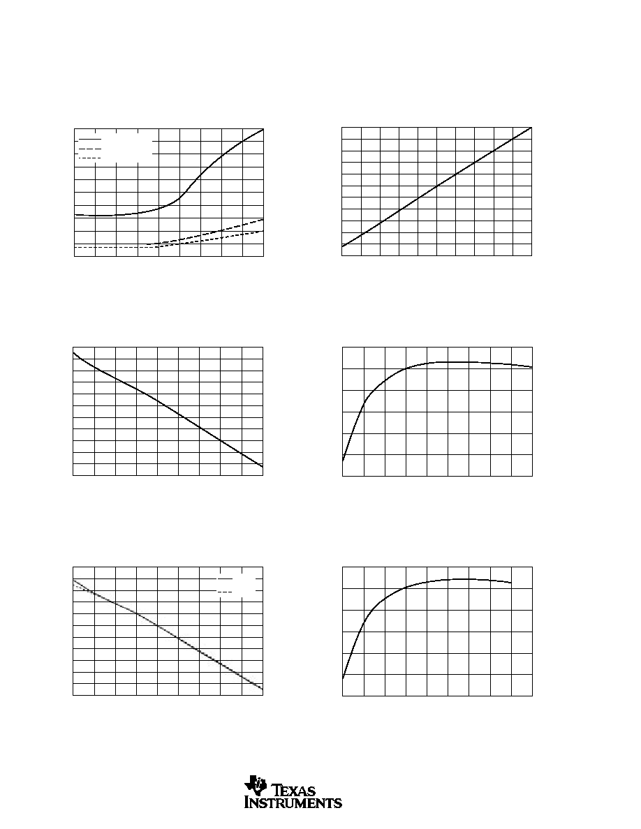
TYPICAL PERFORMANCE CURVES
At T
A
= +25
∞
C, unless otherwise noted.
DCP010505B
OUTPUT RIPPLE vs LOAD (20MHz BW)
Load (%)
Ripple (mVp-p)
50
45
40
35
30
25
20
15
10
5
0
20
30
50
70
60
80
90
100
40
10
1
µ
F Ceramic
4.7
µ
F Ceramic
10
µ
F Ceramic
DCP010505B V
OUT
vs V
S
V
S
(V)
V
OUT
(V)
5.5
5.4
5.3
5.2
5.1
5.0
4.9
4.8
4.7
4.6
4.5
4.4
4.6
4.7
4.9
5.1
5.0
5.2
5.4
5.3
5.5
4.8
4.5
DCP010505B V
OUT
vs LOAD
Load (%)
V
OUT
(V)
5.8
5.7
5.6
5.5
5.4
5.3
5.2
5.1
5.0
4.9
4.8
4.7
100
10
20
30
40
50
60
70
80
90
DCP010505B EFFICIENCY vs LOAD
Load (%)
Ef
ficiency (%)
85
80
75
70
65
60
55
100
10
20
30
40
50
60
70
80
90
DCP010505DB V
OUT
vs LOAD
Load (%)
V
OUT
(V)
5.8
5.7
5.6
5.5
5.4
5.3
5.2
5.1
5.0
4.9
4.8
4.7
100
10
20
30
40
50
60
70
80
90
+V
OUT
≠V
OUT
DCP010505DB EFFICIENCY vs LOAD
Load (%)
Ef
ficiency (%)
85
80
75
70
65
60
55
100
10
20
30
40
50
60
70
80
90

DCP01B
5
SBVS012A
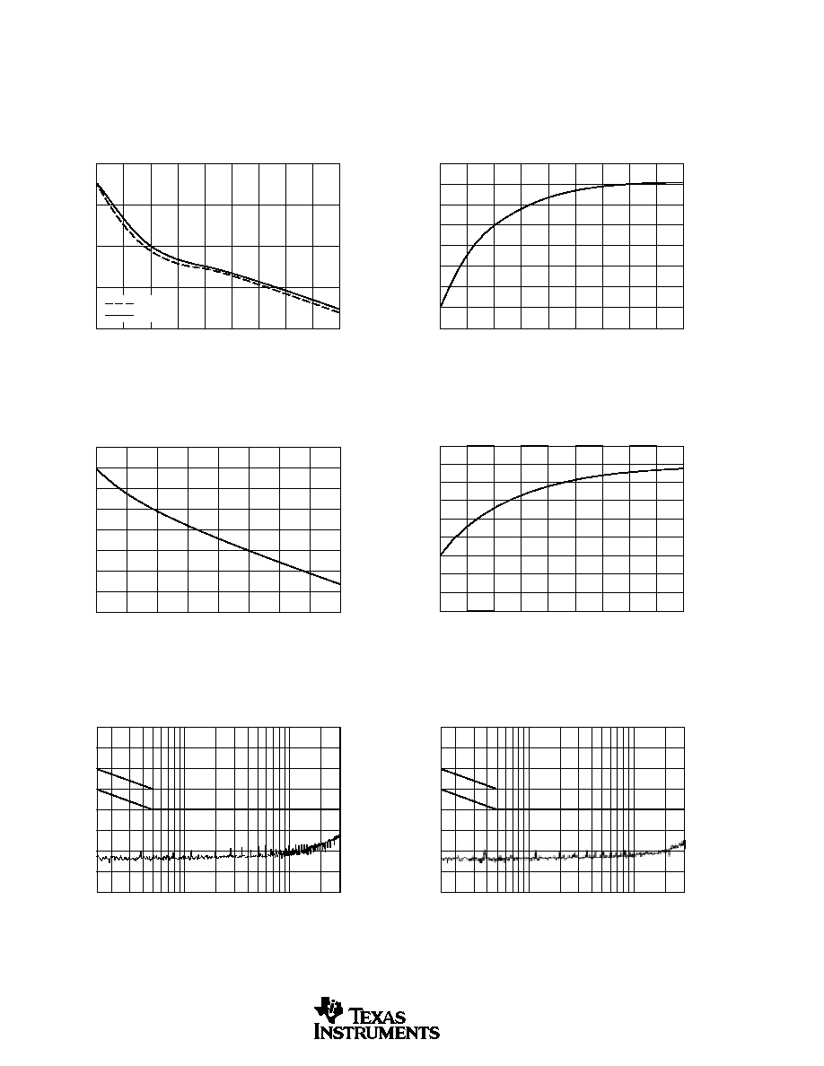
TYPICAL PERFORMANCE CURVES
(Cont.)
At T
A
= +25
∞
C, unless otherwise noted.
DCP010512B V
OUT
vs LOAD
Load (%)
V
OUT
(V)
14.5
14
13.5
13
12.5
12
11.5
11
100
10
20
30
40
50
60
70
80
90
DCP010512B EFFICIENCY vs LOAD
Load (%)
Ef
ficiency (%)
90
85
80
75
70
65
60
55
50
100
10
20
30
40
50
60
70
80
90
DCP010512DB V
OUT
vs LOAD
Load (%)
V
OUT
(V)
14.5
14.0
13.5
13.0
12.5
12.0
11.5
11.0
10.5
10.00
20
30
50
70
60
80
90
100
40
10
+V
OUT
≠V
OUT
DCP010512DB EFFICIENCY vs LOAD
Load (%)
Ef
ficiency (%)
85
80
75
70
65
60
55
50
20
30
50
70
60
80
90
100
40
10
DCP010515B V
OUT
vs LOAD
Load (%)
V
OUT
(V)
18
17.5
17
16.5
16
15.5
15
14.5
14
100
10
20
30
40
50
60
70
80
90
DCP010515B EFFICIENCY vs LOAD
Load (%)
Ef
ficiency (%)
85
80
75
70
65
60
55
50
100
10
20
30
40
50
60
70
80
90
DCP01B
6
SBVS012A
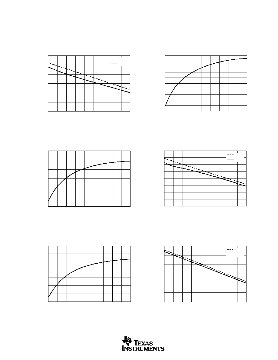
TYPICAL PERFORMANCE CURVES
(Cont.)
At T
A
= +25
∞
C, unless otherwise noted.
DCP010515DB V
OUT
vs LOAD
Load (%)
V
OUT
(V)
18
17
16
15
14
20
30
50
70
60
80
90
100
40
10
+V
OUT
≠V
OUT
DCP010515DB EFFICIENCY vs LOAD
Load (%)
Ef
ficiency (%)
90
85
80
75
70
65
60
55
50
20
30
50
70
60
80
90
100
40
10
DCP012405B V
OUT
vs LOAD
Load (%)
V
OUT
(V)
5.60
5.50
5.40
5.30
5.20
5.10
5.00
4.90
4.80
20
30
60
50
70
80
100
40
10
DCP012405B EFFICIENCY vs LOAD
Load (%)
Ef
ficiency (%)
90
80
70
60
50
40
30
20
10
0
20
30
70
60
80
90
100
40
50
10
DCP010505B
CONDUCTED EMISSIONS (125% Load)
Emission Level, Peak (dB
µ
A)
Frequency (MHz)
1
0.15
10
30
60
50
40
30
20
10
0
≠10
≠20
DCP010505B
CONDUCTED EMISSIONS (8% Load)
Emission Level, Peak (dB
µ
A)
Frequency (MHz)
1
0.15
10
30
60
50
40
30
20
10
0
≠10
≠20
DCP01B
7
SBVS012A
TYPICAL PERFORMANCE CURVES
(Cont.)
At T
A
= +25
∞
C, unless otherwise noted.
DCP011512DBP V
OUT
vs LOAD
Load (%)
V
OUT
(V)
13.50
13.00
12.50
12.00
11.50
11.00
10.50
100
10
20
30
40
50
60
70
80
90
+V
OUT
≠V
OUT
DCP011512DBP
EFFICIENCY vs LOAD
Load (%)
Ef
ficiency (%)
80
75
70
65
60
55
50
45
40
35
30
20
30
50
70
60
80
90
100
40
10
DCP011515DBP
EFFICIENCY vs LOAD
Load (%)
Ef
ficiency (%)
90
80
70
60
50
40
30
100
10
20
30
40
50
60
70
80
90
DCP011515DBP V
OUT
vs LOAD
Load (%)
Ef
ficiency (%)
17.00
16.50
16.00
15.50
15.00
14.50
14.00
13.50
13.00
100
10
20
30
40
50
60
70
80
90
+V
OUT
≠V
OUT
DCP012415DBP EFFICIENCY vs LOAD
Load (%)
Ef
ficiency (%)
90
80
70
60
50
40
30
20
100
10
20
30
40
50
60
70
80
90
DCP012415DBP V
OUT
vs LOAD
Load (%)
V
OUT
(V)
16.50
16.00
15.50
15.00
14.50
14.00
13.50
100
10
20
30
40
50
60
70
80
90
+V
OUT
≠V
OUT
DCP01B
8
SBVS012A
FIGURE 1. Connecting the DCP01B in Series.
FUNCTIONAL DESCRIPTION
OVERVIEW
The DCP01B offers up to 1W of unregulated output power
with a typical efficiency of up to 85%. This is achieved
through highly integrated packaging technology and the
implementation of a custom power stage and control IC. The
circuit design utilizes an advanced BiCMOS/DMOS pro-
cess.
POWER STAGE
This uses a push-pull, center-tapped topology switching at
400kHz (divide by 2 from 800kHz oscillator).
OSCILLATOR AND WATCHDOG
The onboard 800kHz oscillator generates the switching
frequency via a divide by 2 circuit. The oscillator can be
synchronized to other DCP01B circuits or an external source,
and is used to minimize system noise.
A watchdog circuit checks the operation of the oscillator
circuit. The oscillator can be stopped by pulling the SYNC
pin LOW. The output pins will be tri-stated. This will occur
in 2
µ
s.
THERMAL SHUTDOWN
The DCP01B is protected by a thermal shutdown circuit. If
the on-chip temperature exceeds 150
∞
C, the device will shut
down. Once the temperature falls below 150
∞
C, normal
operation will resume.
SYNCHRONIZATION
In the event that more than one DC/DC converter is needed
onboard, beat frequencies and other electrical interference
can be generated. This is due to the small variations in
switching frequencies between the DC/DC converters.
The DCP01B overcomes this by allowing devices to be
synchronized to one another. Up to eight devices can be
synchronized by connecting the SYNC
IN
pins together, tak-
ing care to minimize the capacitance of tracking. Stray
capacitance (> 3pF) will have the effect of reducing the
switching frequency, or even stopping the oscillator circuit.
If synchronized devices are used, it should be noted that, at
start up, all devices will draw maximum current simulta-
neously. This can cause the input voltage to dip and should
it dip below the minimum input voltage (4.5V), the devices
may not start up. A 2.2
µ
F capacitor should be connected
close to the input pins.
If more than eight devices are to be synchronized, it is
recommended that the SYNC
IN
pins are driven by an exter-
nal device. Details are contained in a separate applications
bulletin (AB-153).
CONSTRUCTION
The DCP01B's basic construction is the same as standard
ICs. There is no substrate within the molded package. The
DCP01B is constructed using an IC, rectifier diodes, and a
wound magnetic toroid on a leadframe. As there is no solder
within the package, the DCP01B does not require any
special PCB assembly processing. This results in an isolated
DC/DC converter with inherently high reliability.
ADDITIONAL FUNCTIONS
DISABLE/ENABLE
The DCP01B can be disabled or enabled by driving the SYNC
pin using an open drain CMOS gate. If the SYNC
IN
pin is
pulled low, the DCP01B will be disabled. The disable time
depends upon the external loading; the internal disable func-
tion is implemented in 2
µ
s. Removal of the pull down will
cause the DCP01B to be enabled.
Capacitive loading on the SYNC
IN
pin should be minimized
in order to prevent a reduction in the oscillator frequency.
DECOUPLING
Ripple Reduction
The high switching frequency of 400kHz allows simple
filtering. To reduce ripple, it is recommended that at least a
1
µ
F capacitor is used on V
OUT
. Dual outputs should both be
decoupled to pin 5. A 2.2
µ
F low ESR capacitor on the input
of the 5V in versions, and a 0.47
µ
F low ESR cap on the 24V
DCP01B in versions is recommended.
DCP
01B
V
OUT 1
V
SUPPLY
V
S
0V
DCP
01B
V
OUT 2
V
OUT1
+ V
OUT 2
SYNC
IN
SYNC
IN
V
S
0V
0V
0V
COM
DCP01B
9
SBVS012A
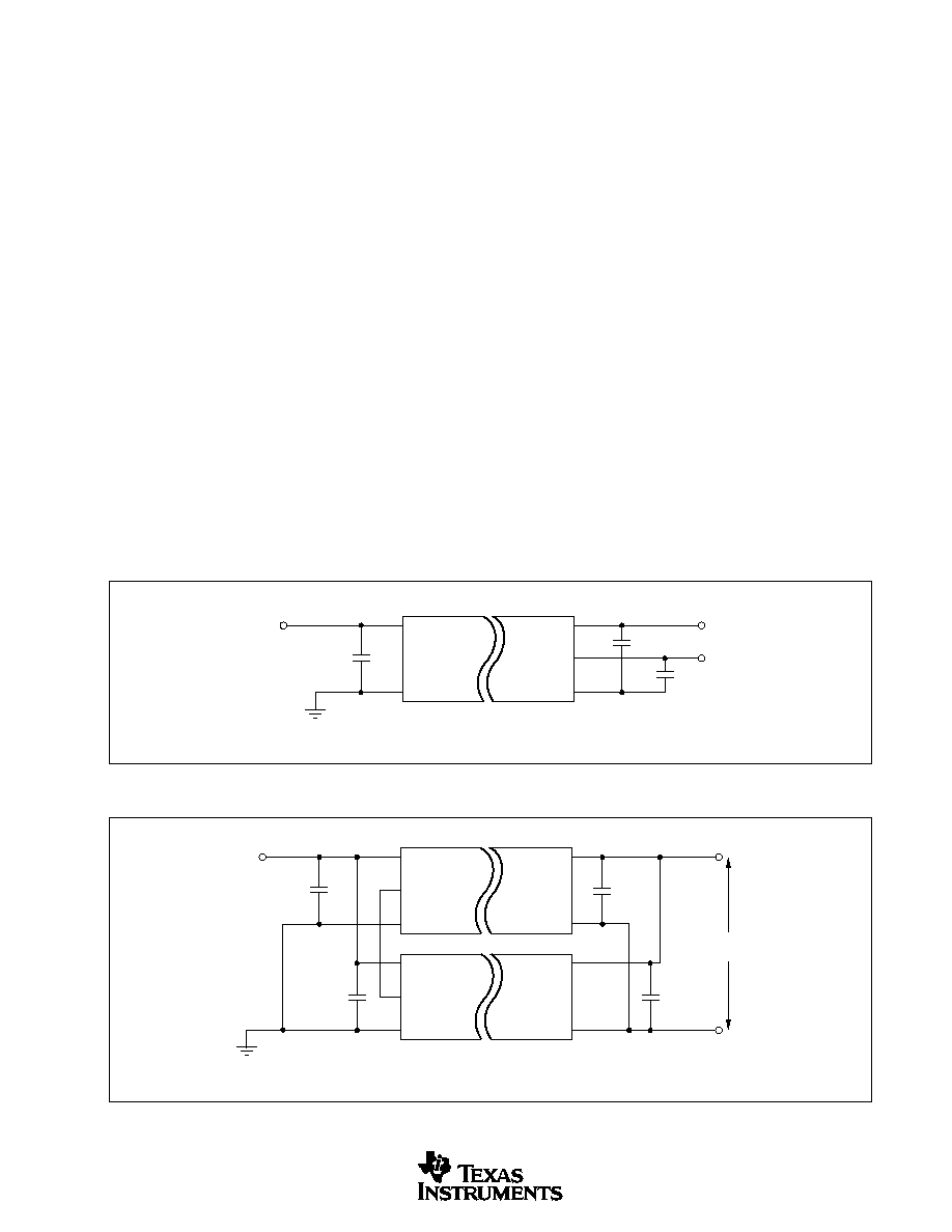
FIGURE 2. Connecting Dual Outputs in Series.
Connecting the DCP01B in Series
Multiple DCP01B isolated 1W DC/DC converters can be
connected in series to provide nonstandard voltage rails.
This is possible by utilizing the floating outputs provided by
the DCP01B's galvanic isolation.
Connect the positive V
OUT
from one DCP01B to the nega-
tive V
OUT
(0V) of another (see Figure 1). If the SYNC
IN
pins
are tied together, the self-synchronization feature of the
DCP01B will prevent beat frequencies on the voltage rails.
The SYNC
IN
feature of the DCP01B allows easy series
connection without external filtering, minimizing cost.
The outputs on dual output DCP01B versions can also be
connected in series to provide two times the magnitude of
V
OUT
as shown in Figure 2. For example, a dual 15V
DCP01B could be connected to provide a 30V rail.
Connecting the DCP01B in Parallel
If the output power from one DCP01B is not sufficient, it is
possible to parallel the outputs of multiple DCP01Bs, as
shown in Figure 3. Again, the SYNC
IN
feature allows easy
synchronization to prevent power-rail beat frequencies at no
additional filtering cost.
PCB LAYOUT
Ripple and Noise
Careful consideration should be given to the layout of the
PCB in order that the best results can be obtained.
The DCP01B is a switching power supply and as such can
place high peak current demands on the input supply. In
order to avoid the supply falling momentarily during the fast
switching pulses ground and power planes should be used to
track the power to the input of DCP01B. If this is not
possible then the supplies must be connected in a star
formation with the tracks made as wide as possible.
If the SYNC
IN
pin is being used then the tracking between
device SYNC
IN
pins should be short to avoid stray capaci-
tance. If the SYNC
IN
pin is not being used it is advisable to
place a guard ring, (connected to input ground) around this
pin to avoid any noise pick up.
The output should be taken from the device using ground
and power planes, this will ensure minimum losses.
A good quality low ESR capacitor placed as close as
practicable across the input will reduce reflected ripple and
ensure a smooth start up.
A good quality low ESR capacitor placed as close as
practicable across the rectifier output terminal and output
ground will give the best ripple and noise performance.
THERMAL MANAGEMENT
Due to the high power density of this device it is advisable
to provide ground planes on the input and output.
FIGURE 3. Connecting Multiple DCP01Bs in Parallel.
DCP
01B
+V
OUT
V
SUPPLY
+V
OUT
≠V
OUT
≠V
OUT
0V
V
S
0V
COM
DCP
01B
0V
0V
V
OUT
V
SUPPLY
V
S
0V
DCP
01B
V
OUT
2 x Power Out
SYNC
IN
SYNC
IN
V
S
0V
COM

PACKAGING INFORMATION
ORDERABLE DEVICE
STATUS(1)
PACKAGE TYPE
PACKAGE DRAWING
PINS
PACKAGE QTY
DCP010505BP
ACTIVE
PDIP
NVA
7
25
DCP010505BP-U
ACTIVE
SOP
DUA
7
25
DCP010505BP-U/700
ACTIVE
SOP
DUA
7
700
DCP010505DBP
ACTIVE
PDIP
NVA
7
25
DCP010505DBP-U
ACTIVE
SOP
DUA
7
25
DCP010505DBP-U/700
ACTIVE
SOP
DUA
7
700
DCP010512BP
ACTIVE
PDIP
NVA
7
25
DCP010512BP-U
ACTIVE
SOP
DUA
7
25
DCP010512BP-U/700
ACTIVE
SOP
DUA
7
700
DCP010512DBP
ACTIVE
PDIP
NVA
7
25
DCP010512DBP-U
ACTIVE
SOP
DUA
7
25
DCP010512DBP-U/700
ACTIVE
SOP
DUA
7
700
DCP010515BP
ACTIVE
PDIP
NVA
7
25
DCP010515BP-U
ACTIVE
SOP
DUA
7
25
DCP010515BP-U/700
ACTIVE
SOP
DUA
7
700
DCP010515DBP
ACTIVE
PDIP
NVA
7
25
DCP010515DBP-U
ACTIVE
SOP
DUA
7
25
DCP010515DBP-U/700
ACTIVE
SOP
DUA
7
700
DCP011512DBP
ACTIVE
PDIP
NVA
7
25
DCP011512DBP-U
ACTIVE
SOP
DUA
7
25
DCP011512DBP-U/700
ACTIVE
SOP
DUA
7
700
DCP011515DBP
ACTIVE
PDIP
NVA
7
25
DCP011515DBP-U
ACTIVE
SOP
DUA
7
25
DCP011515DBP-U/700
ACTIVE
SOP
DUA
7
700
DCP012415DBP
ACTIVE
PDIP
NVA
7
25
DCP012415DBP-U
ACTIVE
SOP
DUA
7
25
DCP012415DBP-U/700
ACTIVE
SOP
DUA
7
700
(1) The marketing status values are defined as follows:
ACTIVE: Product device recommended for new designs.
LIFEBUY: TI has announced that the device will be discontinued, and a lifetime-buy period is in effect.
NRND: Not recommended for new designs. Device is in production to support existing customers, but TI does not recommend using this part in
a new design.
PREVIEW: Device has been announced but is not in production. Samples may or may not be available.
OBSOLETE: TI has discontinued the production of the device.
PACKAGE OPTION ADDENDUM
www.ti.com
3-Oct-2003

IMPORTANT NOTICE
Texas Instruments Incorporated and its subsidiaries (TI) reserve the right to make corrections, modifications,
enhancements, improvements, and other changes to its products and services at any time and to discontinue
any product or service without notice. Customers should obtain the latest relevant information before placing
orders and should verify that such information is current and complete. All products are sold subject to TI's terms
and conditions of sale supplied at the time of order acknowledgment.
TI warrants performance of its hardware products to the specifications applicable at the time of sale in
accordance with TI's standard warranty. Testing and other quality control techniques are used to the extent TI
deems necessary to support this warranty. Except where mandated by government requirements, testing of all
parameters of each product is not necessarily performed.
TI assumes no liability for applications assistance or customer product design. Customers are responsible for
their products and applications using TI components. To minimize the risks associated with customer products
and applications, customers should provide adequate design and operating safeguards.
TI does not warrant or represent that any license, either express or implied, is granted under any TI patent right,
copyright, mask work right, or other TI intellectual property right relating to any combination, machine, or process
in which TI products or services are used. Information published by TI regarding third-party products or services
does not constitute a license from TI to use such products or services or a warranty or endorsement thereof.
Use of such information may require a license from a third party under the patents or other intellectual property
of the third party, or a license from TI under the patents or other intellectual property of TI.
Reproduction of information in TI data books or data sheets is permissible only if reproduction is without
alteration and is accompanied by all associated warranties, conditions, limitations, and notices. Reproduction
of this information with alteration is an unfair and deceptive business practice. TI is not responsible or liable for
such altered documentation.
Resale of TI products or services with statements different from or beyond the parameters stated by TI for that
product or service voids all express and any implied warranties for the associated TI product or service and
is an unfair and deceptive business practice. TI is not responsible or liable for any such statements.
Following are URLs where you can obtain information on other Texas Instruments products and application
solutions:
Products
Applications
Amplifiers
amplifier.ti.com
Audio
www.ti.com/audio
Data Converters
dataconverter.ti.com
Automotive
www.ti.com/automotive
DSP
dsp.ti.com
Broadband
www.ti.com/broadband
Interface
interface.ti.com
Digital Control
www.ti.com/digitalcontrol
Logic
logic.ti.com
Military
www.ti.com/military
Power Mgmt
power.ti.com
Optical Networking
www.ti.com/opticalnetwork
Microcontrollers
microcontroller.ti.com
Security
www.ti.com/security
Telephony
www.ti.com/telephony
Video & Imaging
www.ti.com/video
Wireless
www.ti.com/wireless
Mailing Address:
Texas Instruments
Post Office Box 655303 Dallas, Texas 75265
Copyright
2003, Texas Instruments Incorporated