
Burr Brown Products
from Texas Instruments
DCP02
DCP02
FEATURES
DESCRIPTION
APPLICATIONS
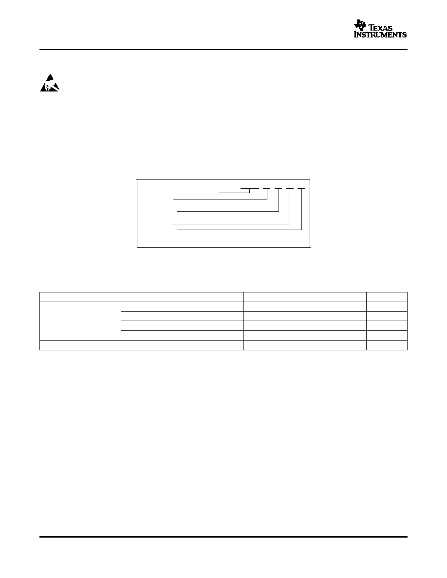
I
BIAS
Power
Stage
V
OUT
Divide-by-2
Reset
800kHz
Oscillator
Watchdog/
Startup
PSU
Thermal
Shutdown
SYNC/DISABLE
V
S
0V
Power Controller IC
0V
DCP02 Series
SBVS011C ≠ MARCH 2000 ≠ REVISED DECEMBER 2005
Miniature, 2W, Isolated
UNREGULATED DC/DC CONVERTERS
∑
Up To 89% Efficiency
The DCP02 series is a family of 2W, isolated,
unregulated DC/DC converters. Requiring a minimum
∑
Thermal Protection
of external components and including on-chip device
∑
Device-to-Device Synchronization
protection, the DCP02 series provides extra features
∑
SO-28 Power Density of 106W/in
3
(6.5W/cm
3
)
such as output disable and synchronization of
∑
EN55022 Class B EMC Performance
switching frequencies.
∑
UL1950 Recognized Component
The use of a highly integrated package design results
in highly reliable products with power densities of
∑
JEDEC 14-Pin and SO-28 Packages
79W/in
3
(4.8W/cm
3
)
for
DIP-14,
and
106W/in
3
(6.5W/cm
3
) for SO-28. This combination of features
and small size makes the DCP02 suitable for a wide
∑
Point-of-Use Power Conversion
range of applications.
∑
Ground Loop Elimination
∑
Data Acquisition
∑
Industrial Control and Instrumentation
∑
Test Equipment
Please be aware that an important notice concerning availability, standard warranty, and use in critical applications of Texas
Instruments semiconductor products and disclaimers thereto appears at the end of this data sheet.
All trademarks are the property of their respective owners.
PRODUCTION DATA information is current as of publication date.
Copyright © 2000≠2005, Texas Instruments Incorporated
Products conform to specifications per the terms of the Texas
Instruments standard warranty. Production processing does not
necessarily include testing of all parameters.
www.ti.com
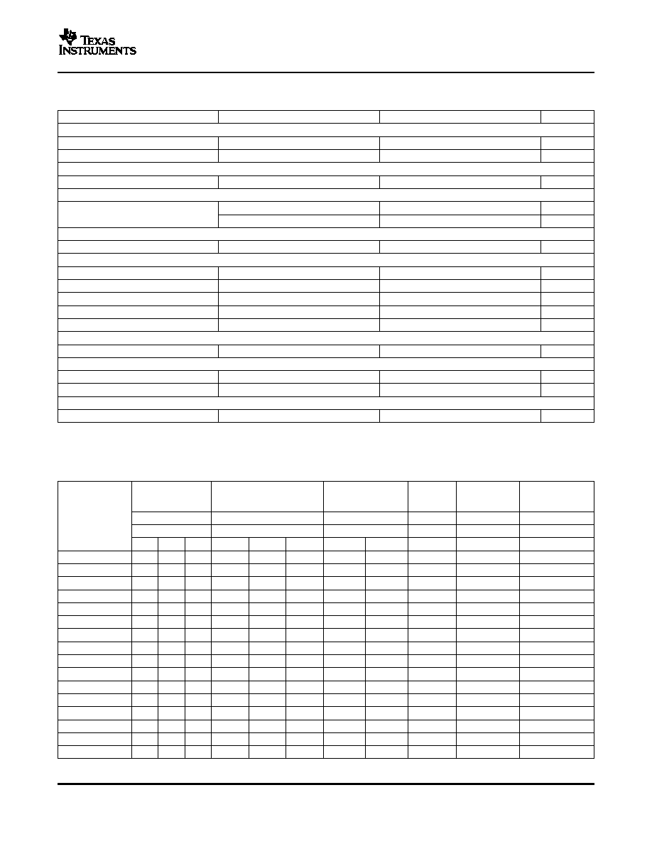
ORDERING INFORMATION
Basic Model Number: 2W Product
Voltage Input:
5V In
Voltage Output:
5V Out
Dual Output:
Package Code:
P = DIP-14
U = SO-28
DCP02
05
05
(D) ( )
ABSOLUTE MAXIMUM RATINGS
DCP02 Series
SBVS011C ≠ MARCH 2000 ≠ REVISED DECEMBER 2005
This integrated circuit can be damaged by ESD. Texas Instruments recommends that all integrated
circuits be handled with appropriate precautions. Failure to observe proper handling and installation
procedures can cause damage.
ESD damage can range from subtle performance degradation to complete device failure. Precision
integrated circuits may be more susceptible to damage because very small parametric changes could
cause the device not to meet its published specifications.
For the most current package and ordering information, see the Package Option Addendum at the end of this
data sheet, or see the TI website at www.ti.com.
Supplemental Ordering Information
over operating free-air temperature range (unless otherwise noted)
(1)
DCP02 Series
UNIT
5V input models
7
V
12V input models
15
V
Input Voltage
15V input models
18
V
24V input models
29
V
Storage temperature range
≠60 to +125
∞
C
(1)
Stresses beyond those listed under Absolute Maximum Ratings may cause permanent damage to the device. These are stress ratings
only, and functional operation of the device at these or any other conditions beyond those indicated under recommended operating
conditions is not implied. Exposure to absolute-maximum-rated conditions for extended periods may affect device reliability.
2
www.ti.com
ELECTRICAL CHARACTERISTICS
ELECTRICAL CHARACTERISTICS PER DEVICE
DCP02 Series
SBVS011C ≠ MARCH 2000 ≠ REVISED DECEMBER 2005
At T
A
= +25
∞
C, unless otherwise noted.
PARAMETER
TEST CONDITIONS
MIN
TYP
MAX
UNIT
OUTPUT
Power
100% full load
2
W
Ripple
O/P capacitor = 1
µ
F, 50% load
20
mV
PP
INPUT
Voltage range on V
S
≠10
10
%
ISOLATION
1s Flash test
1
kVrms
Voltage
60s test, UL1950
(1)
1
kVrms
LINE
Regulation
1
%/1% of V
S
SWITCHING/SYNCHRONIZATION
Oscillator frequency (f
OSC
)
Switching frequency = f
OSC
/2
800
kHz
Sync input low
0
0.4
V
Sync input current
V
SYNC
= +2V
75
µ
A
Disable time
2
µ
s
Capacitance loading on SYNC pin
External
10
pF
RELIABILITY
Demonstrated
T
A
= +55
∞
C
75
FITS
THERMAL SHUTDOWN
IC temperature at shutdown
+150
∞
C
Shutdown current
3
mA
TEMPERATURE RANGE
Operating
≠40
+85
∞
C
(1)
During UL1950 recognition tests only.
At T
A
= +25
∞
C, unless otherwise noted.
INPUT
OUTPUT
LOAD
NO LOAD
BARRIER
VOLTAGE
VOLTAGE
REGULATION
CURRENT
EFFICIENCY
CAPACITANCE
(V)
(V)
(%)
(mA)
(%)
(pF)
V
S
V
NOM
I
Q
C
ISO
75% LOAD
(1)
10% TO 100% LOAD
0% LOAD
100% LOAD
V
ISO
= 750Vrms
PRODUCT
MIN
TYP
MAX
MIN
TYP
MAX
TYP
MAX
TYP
TYP
TYP
DCP020503P, U
4.5
5
5.5
3.13
3.3
3.46
19
30
18
74
26
DCP020505P, U
4.5
5
5.5
4.75
5
5.25
14
20
18
80
22
DCP020507P, U
4.5
5
5.5
6.65
7
7.35
14
25
20
81
30
DCP020509P, U
4.5
5
5.5
8.55
9
9.45
12
20
23
82
31
DCP020515DP, U
4.5
5
5.5
±
14.25
±
15
±
15.75
11
20
27
85
24
DCP021205P, U
10.8
12
13.2
4.75
5
5.25
7
15
14
83
33
DCP021212P, U
10.8
12
13.2
11.4
12
12.6
7
20
15
87
47
DCP021212DP, U
10.8
12
13.2
±
11.4
±
12
±
12.6
6
20
16
88
35
DCP021215DP, U
10.8
12
13.2
±
14.25
±
15
±
15.75
6
20
21
87
33
DCP021515P, U
13.5
15
16.5
14.25
15
15.75
6
20
15
88
42
DCP022405P
21.6
24
26.4
4.85
5
5.35
6
10
13
81
33
DCP022405U
21.6
24
26.4
4.75
5
5.25
10
15
13
81
33
DCP022405DP, U
21.6
24
26.4
±
4.75
±
5
+5.25
6
15
12
80
22
DCP022412DP, U
21.6
24
26.4
±
11.4
±
12
±
12.6
4
16
19
83
29
DCP022415DP, U
21.6
24
26.4
±
14.25
±
15
±
15.75
6
25
16
79
44
DCP022418DP, U
21.6
24
26.4
±
17.1
±
18
±
18.9
9
25
20
84
32
(1)
100% load current = 2W/V
NOM
typ.
3
www.ti.com
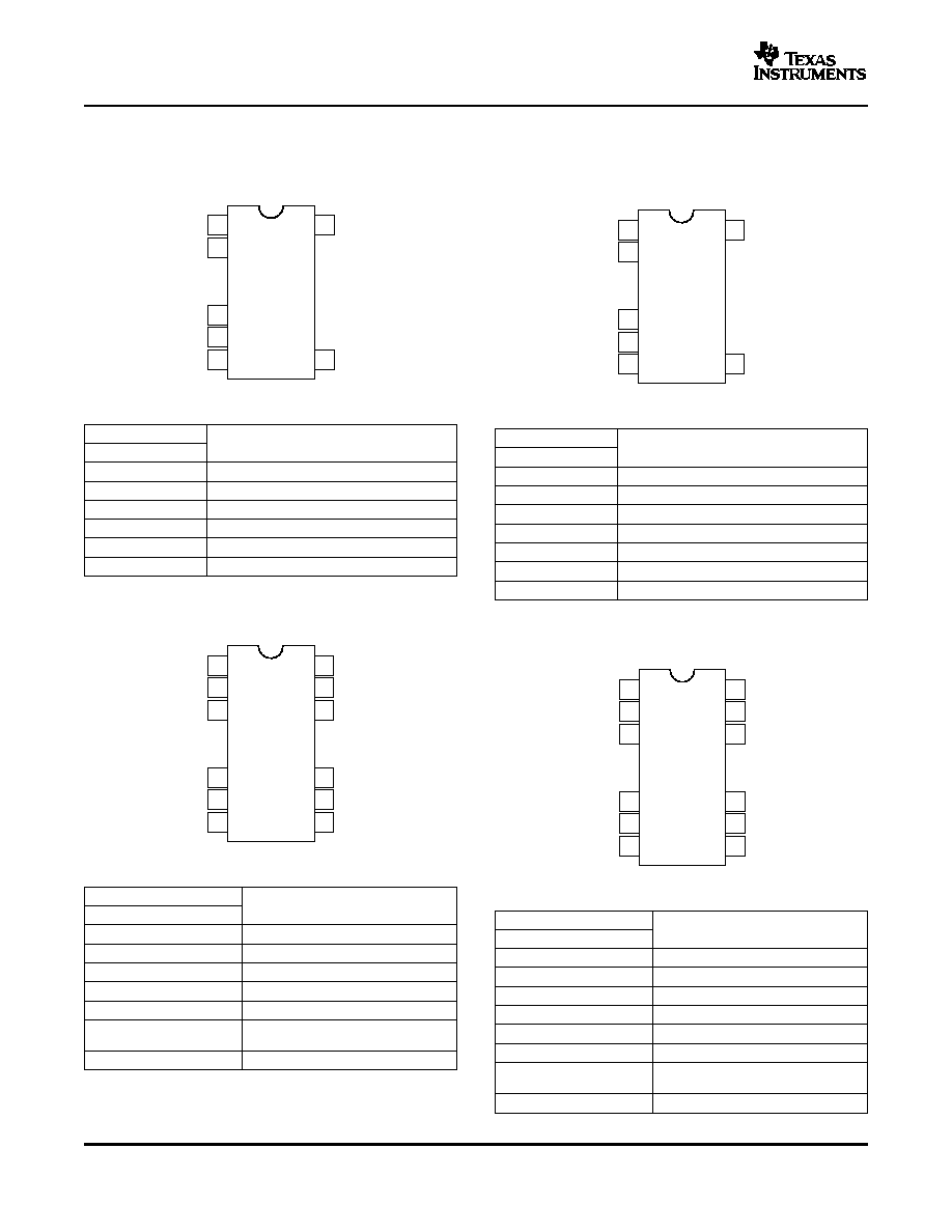
DEVICE INFORMATION
DCP02
1
2
5
6
7
14
8
V
S
0V
0V
+V
OUT
NC
SYNC
NC
DCP02
1
2
5
6
7
14
8
V
S
0V
0V
+V
OUT
-
V
OUT
SYNC
NC
DCP02
1
2
3
12
13
14
28
27
26
17
16
15
V
S
0V
0V
0V
+V
OUT
NC
SYNC
NC
NC
NC
NC
NC
DCP02
1
2
3
12
13
14
28
27
26
17
16
15
V
S
0V
0V
0V
+V
OUT
-
V
OUT
SYNC
NC
NC
NC
NC
NC
DCP02 Series
SBVS011C ≠ MARCH 2000 ≠ REVISED DECEMBER 2005
NVA PACKAGE
NVA PACKAGE
DIP-14 (Single-DIP)
DIP-14 (Dual-DIP)
(Top View)
(Top View)
Table 1. Pin Description (Single-DIP)
Table 3. TERMINAL FUNCTIONS (Dual-DIP)
TERMINAL
TERMINAL
NAME
NO.
DESCRIPTION
NAME
NO.
DESCRIPTION
V
S
1
Voltage input
V
S
1
Voltage input
0V
2
Input side common
0V
2
Input side common
0V
5
Output side common
0V
5
Output side common
+V
OUT
6
+Voltage out
+V
OUT
6
+Voltage out
NC
7, 8
Not connected
≠V
OUT
7
≠Voltage out
SYNC
14
Synchronization pin
NC
8
Not connected
SYNC
14
Synchronization pin
DVB PACKAGE
SO-28 (Single-SO)
DVB PACKAGE
(Top View)
SO-28 (Dual-SO)
(Top View)
Table 2. TERMINAL FUNCTIONS (Single-SO)
TERMINAL
Table 4. TERMINAL FUNCTIONS (Dual-SO)
NAME
NO.
DESCRIPTION
TERMINAL
V
S
1
Voltage input
NAME
NO.
DESCRIPTION
0V
2
Input side common
V
S
1
Voltage input
0V
3
Input side common
0V
2
Input side common
0V
12
Output side common
0V
3
Input side common
+V
OUT
13
+Voltage out
0V
12
Output side common
14, 15, 16,
+V
OUT
13
+Voltage out
NC
Not connected
17, 26, 27
≠V
OUT
14
≠Voltage out
SYNC
28
Synchronization pin
15, 16, 17,
NC
Not connected
26, 27
SYNC
28
Synchronization pin
4
www.ti.com
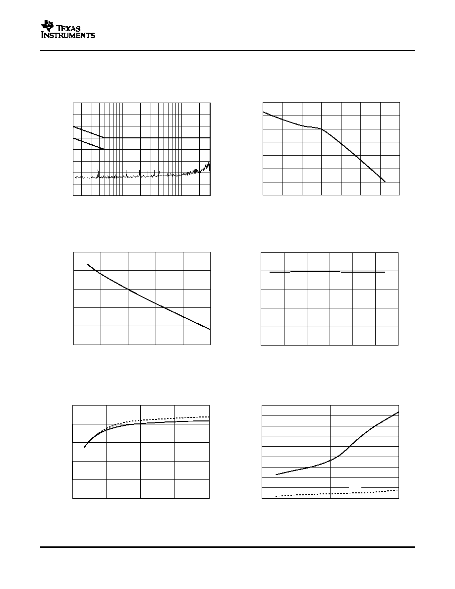
TYPICAL CHARACTERISTICS
Temperature ( C)
∞
V
(V)
O
U
T
5.04
5.02
5.00
4.98
4.96
4.94
4.92
4.90
-20
20
40
60
80
100
0
-40
Emission Level, P
eak (dB
m
A)
Frequency (MHz)
1
0.15
10
30
60
50
40
30
20
10
0
-
10
-
20
5.4
5.3
5.2
5.1
5.0
4.9
Load (%)
V
(V)
O
U
T
0
20
40
60
80
100
Temperature ( C)
∞
P
(W)
O
U
T
0
25
50
75
100
-25
-50
2.5
2.0
1.5
1.0
0.5
0
100
80
60
40
20
0
Load (%)
Efficiency (%)
0
25
50
75
100
DCP1212DP
DCP1205P
450
400
350
300
250
200
150
100
50
0
Load Current (mA)
Ripple (mV
)
PP
0
200
0.1F
400
1F
DCP02 Series
SBVS011C ≠ MARCH 2000 ≠ REVISED DECEMBER 2005
At T
A
= +25
∞
C, unless otherwise noted.
DCP020505P
DCP020505P
CONDUCTED EMISSIONS (500mA Load)
V
OUT
vs TEMPERATURE (75% Load)
Figure 1.
Figure 2.
DCP021205P
DCP021205P
V
OUT
vs LOAD
POWER OUT vs TEMPERATURE (400mA Load)
Figure 3.
Figure 4.
DCP0212
DCP020505P
EFFICIENCY vs LOAD
OUTPUT AC RIPPLE (20MHz Band)
Figure 5.
Figure 6.
5