Document Outline
- FEATURES
- APPLICATIONS
- DESCRIPTION
- ABSOLUTE MAXIMUM RATINGS
- PACKAGE/ORDERING INFORMATION
- ELECTRICAL CHARACTERISTICS
- PIN CONFIGURATION Top View SO
- PIN DESCRIPTIONS
- PIN CONFIGURATION Top View TQFP
- PIN DESCRIPTIONS
- TYPICAL CHARACTERISTICS
- TYPICAL PERFORMANCE CURVES
- THEORY OF OPERATION
- DEVICE OPERATION
- Basic Integration Cycle
- Determining the Integration Capacitor (CF) Value
- Integration Capacitors
- Voltage Reference
- DDC112 Frequency Response
- Test Mode
- DIGITAL ISSUES
- Continuous and Non-Continuous Operational Modes
- TIMING EXAMPLES
- Cont Mode
- Ncont Mode
- Changing Between Modes
- SPECIAL CONSIDERATIONS
- NCONT MODE INTEGRATION TIME
- DATA READY
- Data Retrieval
- Cascading Multiple Converters
- RETRIEVAL BEFORE CONV TOGGLES (CONTINUOUS MODE)
- RETRIEVAL AFTER CONV TOGGLES (CONTINUOUS MODE)
- RETRIEVAL BEFORE AND AFTER CONV TOGGLES (CONTINUOUS MODE)
- RETRIEVAL: NONCONTINUOUS MODE
- POWER-UP SEQUENCING
- LAYOUT
- Power Supplies and Grounding
- Shielding Analog Signal Paths
- PACKAGE DRAWINGS
- DW (R-PDSO-G**) PLASTIC SMALL-OUTLINE PACKAGE
- PJT (S-PQFP N32) PLASTIC QUAD FLATPACK

DDC112
Dual Current Input 20-Bit
ANALOG-TO-DIGITAL CONVERTER
FEATURES
q
MONOLITHIC CHARGE MEASUREMENT ADC
q
DIGITAL FILTER NOISE REDUCTION:
3.2ppm, rms
q
INTEGRAL LINEARITY:
�
0.005% Reading
�
0.5ppm FSR
q
HIGH PRECISION, TRUE INTEGRATING FUNC-
TION
q
PROGRAMMABLE FULL SCALE
q
SINGLE SUPPLY
q
CASCADABLE OUTPUT
APPLICATIONS
q
DIRECT PHOTOSENSOR DIGITIZATION
q
CT SCANNER DAS
q
INFRARED PYROMETER
q
PRECISION PROCESS CONTROL
q
LIQUID/GAS CHROMATOGRAPHY
q
BLOOD ANALYSIS
DESCRIPTION
The DDC112 is a dual input, wide dynamic range, charge-
digitizing analog-to-digital converter (ADC) with 20-bit resolu-
tion. Low level current output devices, such as photosensors,
can be directly connected to its inputs. Charge integration is
continuous as each input uses two integrators; while one is
being digitized, the other is integrating.
For each of its two inputs, the DDC112 combines current-to-
voltage conversion, continuous integration, programmable
full-scale range, A/D conversion, and digital filtering to achieve
a precision, wide dynamic range digital result. In addition to
the internal programmable full-scale ranges, external integrat-
ing capacitors allow an additional user-settable full-scale
range of up to 1000pC.
To provide single-supply operation, the internal ADC utilizes a
differential input, with the positive input tied to V
REF
. When the
integration capacitor is reset at the beginning of each integra-
tion cycle, the capacitor charges to V
REF
. This charge is
removed in proportion to the input current. At the end of the
integration cycle, the remaining voltage is compared to V
REF
.
The high-speed serial shift register which holds the result of
the last conversion can be configured to allow multiple DDC112
units to be cascaded, minimizing interconnections. The
DDC112 is available in a SO-28 or TQFP-32 package and is
offered in two performance grades.
Protected by US Patent #5841310
Dual
Switched
Integrator
Dual
Switched
Integrator
Modulator
Digital
Filter
Control
Digital
Input/Output
DVALID
DXMIT
DOUT
DIN
DCLK
RANGE2
RANGE1
RANGE0
TEST
CONV
CLK
CAP1A
CAP1A
CAP1B
CAP1B
CAP2A
CAP2A
CAP2B
CAP2B
IN2
IN1
V
REF
DGND
DV
DD
AGND
AV
DD
CHANNEL 1
CHANNEL 2
SBAS085A � JANUARY 2000 � REVISED � AUGUST 2002
www.ti.com
PRODUCTION DATA information is current as of publication date.
Products conform to specifications per the terms of Texas Instruments
standard warranty. Production processing does not necessarily include
testing of all parameters.
Copyright � 2000, Texas Instruments Incorporated
Please be aware that an important notice concerning availability, standard warranty, and use in critical applications of
Texas Instruments semiconductor products and disclaimers thereto appears at the end of this data sheet.
DDC112
�
DDC
112
�
DDC112
2
SBAS085A
www.ti.com
AV
DD
to DV
DD
....................................................................... �0.3V to +6V
AV
DD
to AGND ..................................................................... �0.3V to +6V
DV
DD
to DGND ..................................................................... �0.3V to +6V
AGND to DGND ...............................................................................
�
0.3V
V
REF
Voltage to AGND ............................................ �0.3V to AV
DD
+0.3V
Digital Input Voltage to DGND ................................ �0.3V to DV
DD
+0.3V
Digital Output Voltage to DGND ............................. �0.3V to DV
DD
+0.3V
Package Power Dissipation ............................................. (T
JMAX
� T
A
)/
JA
Maximum Junction Temperature (T
JMAX
) ...................................... +150
�
C
Thermal Resistance, SO,
JA
.................................................... +150
�
C/W
Thermal Resistance, TQFP,
JA
................................................ +100
�
C/W
Lead Temperature (soldering, 10s) ............................................... +300
�
C
NOTE: (1) Stresses above those listed under "Absolute Maximum Ratings"
may cause permanent damage to the device. Exposure to absolute maximum
conditions for extended periods may affect device reliability.
ABSOLUTE MAXIMUM RATINGS
(1)
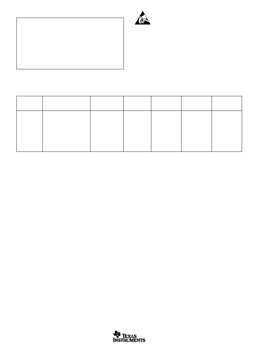
PACKAGE/ORDERING INFORMATION
MAXIMUM
SPECIFICATION
INTEGRAL
TEMPERATURE
PACKAGE
ORDERING
TRANSPORT
PRODUCT
LINEARITY ERROR
RANGE
PACKAGE-LEAD
DESIGNATOR
(1)
NUMBER
(2)
MEDIA
DDC112U
�
0.025% Reading
�
1.0ppm FSR
�40
�
C to +85
�
C
SO-28
DW
DDC112U
Rails
"
"
"
"
"
DDC112U/1K
Tape and Reel
DDC112UK
�
0.025% Reading
�
1.0ppm FSR
0
�
C to +70
�
C
SO-28
DW
DDC112UK
Rails
"
"
"
"
"
DDC112UK/1K
Tape and Reel
DDC112Y
�
0.025% Reading
�
1.0ppm FSR
�40
�
C to +85
�
C
TQFP-32
PJT
DDC112Y/250
Tape and Reel
"
"
"
"
"
DDC112Y/2K
Tape and Reel
DDC112YK
�
0.025% Reading
�
1.0ppm FSR
0
�
C to +70
�
C
TQFP-32
PJT
DDC112YK/250
Tape and Reel
"
"
"
"
"
DDC112YK/2K
Tape and Reel
NOTES: (1) For the most current specifications and and package information, refer to our web site at www.ti.com. (2)Models with a slash (/) are available only in Tape
and Reel in the quantities indicated (e.g., /1K indicates 1000 devices per reel). Ordering 1000 pieces of "DDC112U/1K" will get a single 1000-piece Tape and Reel.
ELECTROSTATIC
DISCHARGE SENSITIVITY
This integrated circuit can be damaged by ESD. Texas Instru-
ments recommends that all integrated circuits be handled with
appropriate precautions. Failure to observe proper handling
and installation procedures can cause damage.
ESD damage can range from subtle performance degradation
to complete device failure. Precision integrated circuits may be
more susceptible to damage because very small parametric
changes could cause the device not to meet its published
specifications.

DDC112
3
SBAS085A
www.ti.com
ELECTRICAL CHARACTERISTICS
At T
A
= +25
�
C, AV
DD
= DV
DD
= +5V, DDC112U, Y: T
INT
= 500
�
s, CLK = 10MHz, DDC112UK, YK: T
INT
= 333.3
�
s, CLK = 15MHz, V
REF
= +4.096V, continuous mode
operation, and internal integration capacitors, unless otherwise noted.
NOTES: (1) Input is less than 1% of full scale. (2) C
SENSOR
is the capacitance seen at the DDC112 inputs from wiring, photodiode, etc. (3) FSR is Full-Scale Range.
(4) A best-fit line is used in measuring linearity. (5) Matching between side A and side B, not input 1 to input 2. (6) Voltage produced by the DDC112 at its input which
is applied to the sensor. (7) Range drift does not include external reference drift. (8) Input reference current decreases with increasing T
INT
(see text). (9) Data format
is Straight Binary with a small offset (see text). (10) Guaranteed but not tested.
DDC112U, Y
DDC112UK, YK
PARAMETER
CONDITIONS
M I N
T Y P
MAX
M I N
T Y P
MAX
UNITS
ANALOG INPUTS
External, Positive Full-Scale
Range 0
C
EXT
= 250pF
1000
pC
Internal, Positive Full-Scale
Range 1
47.5
50
52.5
pC
Range 2
95
100
105
pC
Range 3
142.5
150
157.5
pC
Range 4
190
200
210
pC
Range 5
237.5
250
262.5
pC
Range 6
285
300
315
pC
Range 7
332.5
350
367.5
pC
Negative Full-Scale Input
�0.4% of Positive FS
pC
DYNAMIC CHARACTERISTICS
Conversion Rate
2
3
kHz
Integration Time, T
INT
Continuous Mode
500
1,000,000
333.3
�
s
Integration Time, T
INT
Non-continuous Mode
50
�
s
System Clock Input (CLK)
1
10
12
15
MHz
Data Clock (DCLK)
12
15
MHz
ACCURACY
Noise, Low Level Current Input
(1)
C
SENSOR
(2)
= 0pF, Range 5 (250pC)
3.2
ppm of FSR
(3)
, rms
C
SENSOR
= 25pF, Range 5 (250pC)
3.8
ppm of FSR, rms
C
SENSOR
= 50pF, Range 5 (250pC)
4.2
6.0
7
ppm of FSR, rms
Differential Linearity Error
�
0.005% Reading
�
0.5ppm
FSR, max
Integral Linearity Error
(4)
�
0.005% Reading
�
0.5ppm
FSR, typ
�
0.025% Reading
�
1.0ppm
FSR, max
No Missing Codes
20
Bits
Input Bias Current
T
A
= +25
�
C
0.1
10
pA
Range Error
Range 5 (250pC)
5
% of FSR
Range Error Match
(5)
All Ranges
0.1
0.5
% of FSR
Range Sensitivity to V
REF
V
REF
= 4.096
�
0.1V
1:1
Offset Error
Range 5, (250pC)
�
200
�
600
ppm of FSR
Offset Error Match
(5)
�
100
ppm of FSR
DC Bias Voltage
(6)
(Input V
OS
)
�
0.05
�
2
mV
Power Supply Rejection Ratio
�
25
�
200
ppm of FSR/V
Internal Test Signal
13
pC
Internal Test Accuracy
�
10
%
PERFORMANCE OVER TEMPERATURE
Offset Drift
�
0.5
�
3
(10)
ppm of FSR/
�
C
Offset Drift Stability
�
0.2
�
0.7
(10)
ppm of FSR/minute
DC Bias Voltage Drift
Applied to Sensor Input
3
�
1
�
V/
�
C
Input Bias Current Drift
+25
�
C to +45
�
C
0.01
1
(10)
pA/
�
C
Input Bias Current
T
A
= +75
�
C
2
50
(10)
pA
Range Drift
(7)
Range 5 (250pC)
25
0
25
50
(10)
ppm/
�
C
Range Drift Match
(5)
Range 5 (250pC)
�
0.05
ppm/
�
C
REFERENCE
Voltage
4.000
4.096
4.200
V
Input Current
(8)
T
INT
= 500
�
s
150
225
275
�
A
DIGITAL INPUT/OUTPUT
Logic Levels
V
IH
4.0
DV
DD
+ 0.3
V
V
IL
�0.3
+0.8
V
V
OH
I
OH
= �500
�
A
4.5
V
V
OL
I
OL
= 500
�
A
0.4
V
Input Current, I
IN
�10
+10
�
A
Data Format
(9)
Straight Binary
POWER SUPPLY REQUIREMENTS
Power Supply Voltage
AV
DD
and DV
DD
4.75
5.25
V
Supply Current
Analog Current
AV
DD
= +5V
14.8
15.2
mA
Digital Current
DV
DD
= +5V
1.2
1.8
mA
Total Power Dissipation
80
100
85
130
mW
TEMPERATURE RANGE
Specified Performance
�40
+85
0
+70
�
C
Storage
�60
+100
�
C

DDC112
4
SBAS085A
www.ti.com
PIN DESCRIPTIONS
PIN
LABEL
DESCRIPTION
1
IN1
Input 1: analog input for Integrators 1A and 1B. The
integrator that is active is set by the CONV input.
2
AGND
Analog Ground.
3
CAP1B
External Capacitor for Integrator 1B.
4
CAP1B
External Capacitor for Integrator 1B.
5
CAP1A
External Capacitor for Integrator 1A.
6
CAP1A
External Capacitor for Integrator 1A.
7
AV
DD
Analog Supply, +5V nominal.
8
TEST
Test Control Input. When HIGH, a test charge is
applied to the A or B integrators on the next CONV
transition.
9
CONV
Controls which side of the integrator is connected to
input. In continuous mode; CONV HIGH
side A is
integrating, CONV LOW
side B is integrating.
CONV must be synchronized with CLK (see text).
10
CLK
System Clock Input, 10MHz nominal.
11
DCLK
Serial Data Clock Input. This input operates the
serial I/O shift register.
12
DXMIT
Serial Data Transmit Enable Input. When LOW, this
input enables the internal serial shift register.
13
DIN
Serial Digital Input. Used to cascade multiple
DDC112s.
14
DV
DD
Digital Supply, +5V nominal.
15
DGND
Digital Ground.
16
DOUT
Serial Data Output, Hi-Z when DXMIT is HIGH.
17
DVALID
Data Valid Output. A LOW value indicates valid data
is available in the serial I/O register.
18
RANGE0
Range Control Input 0 (least significant bit).
19
RANGE1
Range Control Input 1.
20
RANGE2
Range Control Input 2 (most significant bit).
21
AGND
Analog Ground.
22
V
REF
External Reference Input, +4.096V nominal.
23
CAP2A
External Capacitor for Integrator 2A.
24
CAP2A
External Capacitor for Integrator 2A.
25
CAP2B
External Capacitor for Integrator 2B.
26
CAP2B
External Capacitor for Integrator 2B.
27
AGND
Analog Ground.
28
IN2
Input 2: analog input for Integrators 2A and 2B. The
integrator that is active is set by the CONV input.
PIN CONFIGURATION
Top View
SO
1
2
3
4
5
6
7
8
9
10
11
12
13
14
28
27
26
25
24
23
22
21
20
19
18
17
16
15
IN2
AGND
CAP2B
CAP2B
CAP2A
CAP2A
V
REF
AGND
RANGE2 (MSB)
RANGE1
RANGE0 (LSB)
DVALID
DOUT
DGND
IN1
AGND
CAP1B
CAP1B
CAP1A
CAP1A
AV
DD
TEST
CONV
CLK
DCLK
DXMIT
DIN
DV
DD
DDC112U

DDC112
5
SBAS085A
www.ti.com
CAP1A
CAP1A
AV
DD
NC
NC
TEST
CONV
CLK
CAP2A
CAP2A
V
REF
AGND
NC
NC
RANGE2 (MSB)
RANGE1
1
2
3
4
5
6
7
8
24
23
22
21
20
19
18
17
DDC112Y
CAP1B
CAP1B
AGND
IN1
IN2
AGND
CAP2B
CAP2B
32
31
30
29
28
27
26
25
DCLK
DXMIT
DIN
DV
DD
DGND
DOUT
DVALID
RANGE0 (LSB)
9
10
11
12
13
14
15
16
PIN CONFIGURATION
Top View
TQFP
PIN DESCRIPTIONS
PIN
LABEL
DESCRIPTION
1
CAP1A
External Capacitor for Integrator 1A.
2
CAP1A
Exteranl Capacitor for Integrator 1A.
3
AV
DD
Analog Supply, +5V nominal.
4
NC
No Connection
5
NC
No Connection
6
TEST
Test Control Input. When HIGH, a test charge is
applied to the A or B integrators on the necxt CONV
transition.
7
CONV
Controls which side of the integrator is connedted to
input. In continuous mode; CONV HIGH side A is
integrating, CONV LOW side B is integrating CONV
must be synchronized with CLK (see text).
8
CLK
System Clock Input, 10MHz nominal
9
DCLK
Serial Data Clock Input. This input operates the
serial I/O shift register.
10
DXMIT
Serial Data Transmit Enable Input. When LOW, this
input enables the internal serial shift register.
11
DIN
Serial Digital Input. Used to cascade multiple
DDC112s.
12
DV
DD
Digital Supply, +5V nominal.
13
DGND
Digital Ground
14
DOUT
Serial Data Output, Hi-Z when DXMIT is HIGH.
PIN
LABEL
DESCRIPTION
15
DVALID
Data Valid Output. A LOW value indicates valid data is
available in the serial I/O register.
16
RANGE0
Range Control Input 0 (least significant bit).
17
RANGE1
Range Control Input 1.
18
RANGE2
Range Control Input 2. (most significant bit).
19
NC
No Connection
20
NC
No Connection
21
AGND
Analog Ground.
22
V
REF
External Reference Input, +4.096V nominal.
23
CAP2A
External Capacitor for Integrator 2A.
24
CAP2A
External Capacitor for Integrator 2A.
25
CAP2B
External Capacitor for Integrator 2B.
26
CAP2B
Exteranl Capacitor for Integrator 2B.
27
AGND
Analog Ground.
28
IN2
Input 2: analog input for Integrators 2A and 2B. The
integrator that is active is set by the CONV input.
29
IN1
Input 1: analog input for Integrators 1A and 1B. The
integrator that is active is set by the CONV input.
30
AGND
Analog Ground.
31
CAP1B
External Capacitor for Integrator 1B.
32
CAP1B
External Capacitor for Integrator 1B.