 | –≠–ª–µ–∫—Ç—Ä–æ–Ω–Ω—ã–π –∫–æ–º–ø–æ–Ω–µ–Ω—Ç: DF1760P | –°–∫–∞—á–∞—Ç—å:  PDF PDF  ZIP ZIP |
FEATURES
q
DUAL 20-BIT MONOLITHIC MODULATOR
(PCM1760) AND MONOLITHIC
DECIMATING DIGITAL FILTER (DF1760)
q
HIGH PERFORMANCE:
THD+N: ≠92dB typ, ≠90dB max
Dynamic Range: 108dB typ
SNR: 108dB min, 110dB typ
Channel Separation: 98dB typ, 94dB min
q
64X OVERSAMPLING
q
CO-PHASE CONVERSION
q
RUNS ON 256fs OR 384fs SYSTEM
CLOCK
q
VERSATILE INTERFACE CAPABILITY:
16-, 20-Bit Output
MSB First or LSB First Format
q
OPTIONAL FUNCTIONS:
Offset Error Calibration
Overflow Detection
Power Down Mode (DF1760)
q
RUNS ON
±
5V SUPPLIES (PCM1760) AND
5V SUPPLY (DF1760)
q
COMPACT 28-PIN PACKAGES:
28-Pin DIP and SOIC
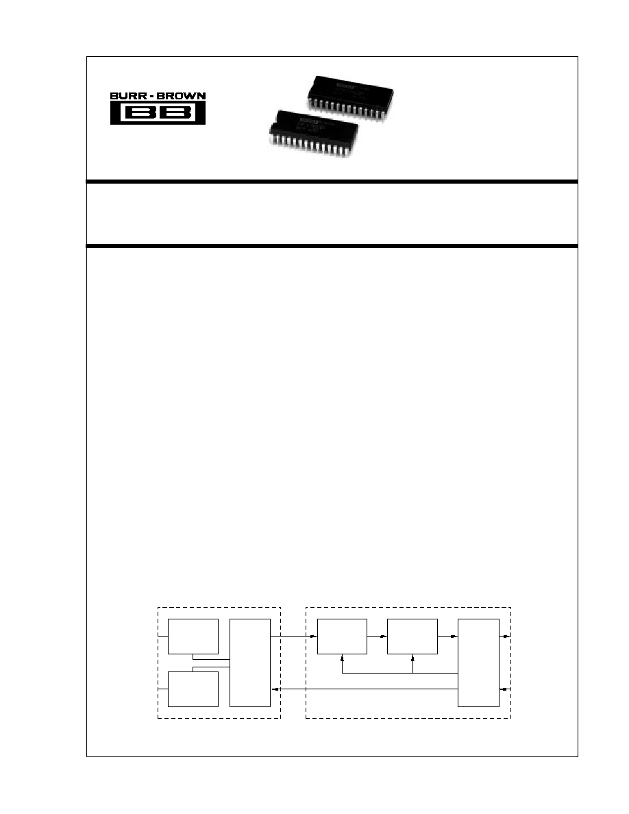
Multi-Bit Enhanced Noise Shaping 20-Bit
ANALOG-TO-DIGITAL CONVERSION SYSTEM
DESCRIPTION
The PCM1760 and DF1760 combine for a low-cost,
high-performance dual 20-bit, 48kHz sampling ana-
log-to-digital conversion system which is specifically
designed for dynamic applications.
The PCM1760/DF1760 pair form a 4-bit, 4th order,
64X oversampling analog-to-digital converter.
The PCM1760 is a delta-sigma modulator that uses a
4-bit quantizer within the modulation loop to achieve
very high dynamic range.
The DF1760 is a high-performance decimating digital
filter. The DF1760 accepts 4-bit 64fs data from the
PCM1760 and decimates to 20-bit 1fs data.
The FIR filter of the DF1760 has pass-band ripple of
less than
±
0.001dB and greater than 100dB of the
reject band attenuation.
4 Stage, 4-Bit
Delta-Sigma
Modulator
4 Stage, 4-Bit
Delta-Sigma
Modulator
Timing
Control
and
Interface
1/16
Filter
FIR
Filter
Timing
Control
and
Interface
PCM1760
Analog
Input (L)
Analog
Input (R)
64fs
256fs
4fs
fs
Data
System
Clock
256/384fs
64fs
DF1760
International Airport Industrial Park ∑ Mailing Address: PO Box 11400 ∑ Tucson, AZ 85734 ∑ Street Address: 6730 S. Tucson Blvd. ∑ Tucson, AZ 85706
Tel: (520) 746-1111 ∑ Twx: 910-952-1111 ∑ Cable: BBRCORP ∑ Telex: 066-6491 ∑ FAX: (520) 889-1510 ∑ Immediate Product Info: (800) 548-6132
PCM1760P/U
DF1760P/U
Æ
©
1993 Burr-Brown Corporation
PDS-1174C
Printed in U.S.A. July, 1994
SBAS025
Æ
PCM1760P/U DF1760P/U
2
SPECIFICATIONS
ELECTRICAL
At T
A
= +25
∞
C,
±
V
CC
,
±
V
dd
= +5V, +V
DD
= +5V, f
S
= 48kHz and ext. components =
±
2% unless otherwise noted.
PCM1760/DF1760
PARAMETER
CONDITIONS
MIN
TYP
MAX
UNITS
RESOLUTION
20
Bits
ANALOG INPUT
Input Range
R
IN
1 = 2.2k
±
2.5
Vp-p
Input Impedance
R
IN
1 = 2.2k
R
IN
1
SAMPLING FREQUENCY
Cover Range of fs
Integrator Constants: Application
(1)
30
48
50
kHz
ACCURACY
Gain Error
±
0.5
±
1.0
dB
Gain Mismatch
±
0.5
dB
Bipolar Zero Error
V
IN
= 0 at 20s After Power-On
±
0.4
% FSR
(2)
Gain Drift
0
∞
C to +70
∞
C
±
100
ppmfs/
∞
C
Bipolar Zero Drift
0
∞
C to +70
∞
C
±
20
ppmfs/
∞
C
DYNAMIC CHARACTERISTICS
(4)
THD+N/(0dBFS)
P, U
f
IN
= 1kHz
≠92
≠90
dB
P-L, U-L
≠90
≠88
dB
THD+N/(≠20dBFS)
P, U
f
IN
= 1kHz
≠76
≠70
dB
P-L, U-L
≠76
≠70
dB
THD+N/(≠60dBFS)
P, U
f
IN
= 1kHz
≠44
≠42
dB
P-L, U-L
≠44
≠42
dB
Dynamic Range
P, U
f
IN
= 1kHz, V
IN
= ≠60dBFS, A Filter
104
108
dB
P-L, U-L
104
108
dB
SNR
P, U
V
IN
= 0, A Filter
108
110
dB
P-L, U-L
106
110
dB
Frequency Response
f
IN
= 20kHz
±
0.1
dB
Channel Separation
f
IN
= 1kHz, A Filter
94
98
dB
DIGITAL FILTER
Over Sample Rate
64
fs
Ripple in Band
0 - 0.04535fs
±
0.0001
dB
Stopband Attenuation ≠1
0.5465fs - 63.4535fs
≠94
dB
Stopband Attenuation ≠2
0.5465fs - 3.4535fs
≠100
dB
LOGIC INPUTS AND OUTPUTS
Logic Family Input
TTL Level Compatible CMOS
Frequency (System Clock 1)
256fs
12.288
MHz
Frequency (System Clock 2)
384fs
18.432
MHz
Duty Cycle (System Clock 1)
256fs
40
50
60
%
Duty Cycle (System Clock 2)
384fs
45
50
55
%
Data Clock Input
32
48
64
fs
Logic Family Output
CMOS
Data Clock Output
64
fs
Data Coding
Two's Complement
Data Bit Length
16
20
Bits
Data Format
Selectable
Output Data Delay
fs = 48kHz
1.5
ms
POWER SUPPLY REQUIREMENTS
Supply Voltage
±
V
CC
PCM1760
±
4.75
±
5.0
±
5.25
V
±
V
dd
PCM1760
±
4.75
±
5.0
±
5.25
V
+V
DD
DF1760
4.75
5.0
5.25
V
Supply Current
+I
CC
PCM1760
24
36
mA
≠I
CC
PCM1760
≠30
≠45
mA
+I
dd
PCM1760
12
18
mA
≠I
DD
PCM1760
≠8
≠12
mA
+I
DD
≠1
DF1760, Normal Mode
40
55
mA
+I
DD
≠2
DF1760, Power-Down Mode
4
6.6
mA
Power Consumption
PCM1760
370
500
mW
DF1760, Normal Mode
200
275
mW
DF1760, Power-Down Mode
20
33
mW
TEMPERATURE RANGE
Operating
PCM1760/DF1760
0
+25
+70
∞
C
Storage
PCM1760/DF1760
≠50
+125
∞
C
NOTES: (1) Integrator Constants are determined by the external components shown in the block diagram. (2) FSR means Full Scale Range, digital output code is from
90000H to 70000H, FSR = 5.0V. (3) Use 20-bit DAC, 20kHz LPF, 400Hz HPF, average response. (4) Average response using a 20-bit reconstruction DAC with 20kHz
low-pass filter and 400Hz high-pass filter.
Æ
3
PCM1760P/U DF1760P/U
MODEL
PACKAGE
THD +N (fs)
SNR
PCM1760P
PDIP
≠90dB
108dB
PCM1760U
SOIC
≠90dB
108dB
PCM1760P-L
PDIP
≠88dB
106dB
PCM1760U-L
SOIC
≠88dB
106dB
DF1760P
PDIP
NA
NA
DF1760U
SOIC
NA
NA
Supply Voltage .................................................................................... 7.0V
Voltage Mismatch ............................................................................... 0.1V
Digital Input ............................................................................... +V
DD
+0.5V
V
SS
≠0.5V
Input Current
±
20mA
Power Dissipation/P ....................................................................... 460mW
Power Dissipation/U ....................................................................... 440mW
Lead Temperature/P (soldering, 10s) .............................................. 260
∞
C
Lead Temperature/U (soldering, 10s, reflow) ................................... 235
∞
C
Operating Temperature .......................................................... 0
∞
C to +70
∞
c
Storage Temperature ...................................................... ≠50
∞
C to +125
∞
C
Supply Voltage .....................................................................................
±
6V
Voltage Mismatch ............................................................................... 0.1V
Analog Input ........................................................................................
±
V
CC
Digital Input ............................................................................... +V
DD
+0.3V
GND ≠0.3V
Power Dissipation/P ....................................................................... 580mW
Power Dissipation/U ....................................................................... 550mW
Lead Temperature/P (soldering, 10s) .............................................. 260
∞
C
Lead Temperature/U (soldering, 10s) .............................................. 235
∞
C
Operating Temperature ......................................................... 0
∞
C to +70
∞
C
Storage Temperature ...................................................... ≠50
∞
C to +125
∞
C
ABSOLUTE MAXIMUM RATINGS--PCM1760
ABSOLUTE MAXIMUM RATINGS--DF1760
The information provided herein is believed to be reliable; however, BURR-BROWN assumes no responsibility for inaccuracies or omissions. BURR-BROWN
assumes no responsibility for the use of this information, and all use of such information shall be entirely at the user's own risk. Prices and specifications are subject
to change without notice. No patent rights or licenses to any of the circuits described herein are implied or granted to any third party. BURR-BROWN does not
authorize or warrant any BURR-BROWN product for use in life support devices and/or systems.
ORDERING INFORMATION
PACKAGE INFORMATION
PACKAGE DRAWING
MODEL
PACKAGE
NUMBER
(1)
PCM1760P
28-Pin PDIP
800
PCM1760U
28-Pin SOIC
804
PCM1760P-L
28-Pin PDIP
800
PCM1760U-L
28-Pin SOIC
804
DF1760P
28-Pin PDIP
801
DF1760U
28-Pin SOIC
805
NOTE: (1) For detailed drawing and dimension table, please see end of data
sheet, or Appendix D of Burr-Brown IC Data Book.
PIN ASSIGNMENTS PCM1760
PIN
I/O
(1)
NAME
DESCRIPTION
1
O
Out-2R
Right Channel Second Integrator Output
2
I
In-2R
Right Channel Second Integrator Input
3
O
Out-1R
Right Channel First Integrator Output
4
I
In-1R
Right Channel First Integrator Input
5
≠
SERVO DC
Servo Amp Decoupling Capacitor
6
≠
+V
CC
+5V Analog Supply Voltage
7
≠
AGND
Analog Common
8
≠
≠V
CC
≠5V Analog Supply Voltage
9
≠
BGDC
Band Gap Reference Decoupling Capacitor
10
≠
NC
No Connection
11
I
In-1L
Left Channel First Integrator Input
12
O
Out-1L
Left Channel First Integrator Output
13
I
In-2L
Left Channel Second Integrator Input
14
O
Out-2L
Left Channel Second Integrator Output
15
≠
NC
No Connection
16
≠
BPODC-L
Left Channel Bipolar Offset Decoupling Capacitor
17
O
L/RCK
LR Clock Output (64fs)
18
O
Strobe
Data Strobe Output (128fs)
19
I
256fs
256fs Clock Input
20
≠
≠V
DD
≠5V Digital Supply Voltage
21
≠
DGND
Digital Common
22
≠
+V
DD
+5V Digital Supply Voltage
23
O
D
0
D
0
Data Output (LSB)
24
O
D
1
D
1
Data Output
25
O
D
2
D
2
Data Output
26
O
D
3
D
3
Data Output (MSB)
27
≠
BPODC-R
Right Channel Bipolar Offset Decoupling Capacitor
28
≠
NC
No Connection
Top View
SOIC/DIP
PCM1760
28
27
26
25
24
23
22
21
20
19
18
17
16
15
Out-2R
In-2R
Out-1R
In-1R
SERVO DC
+V
CC
AGND
≠V
CC
BGDC
NC
In-1L
Out-1L
In-2L
Out-2L
NC
BPODC-R
D
3
D
2
D
1
D
0
+V
DD
DGND
≠V
DD
256fs
Strobe
L/RCK
BPODC-L
NC
1
2
3
4
5
6
7
8
9
10
11
12
13
14
NOTE: (1) O = Output terminal; I = Input terminal.
Æ
PCM1760P/U DF1760P/U
4
Top View
SOIC/DIP
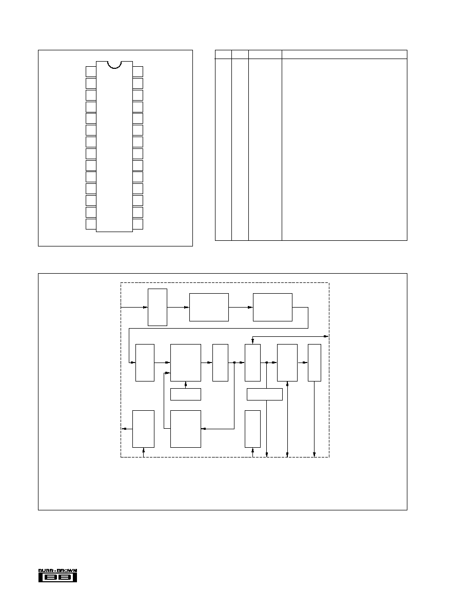
BLOCK DIAGRAM OF DF1760
DF1760
28
27
26
25
24
23
22
21
20
19
18
17
16
15
OVL
OVR
D
3
D
2
D
1
D
0
TP1
V
SS1
V
DD1
256fs
Strobe
LRCK
CALD
CAL
V
SS2
V
DD2
TP2
CLKSEL
S/M
Mode 1
Mode 2
/PD
LRSC
FSYNC
SDATA
L/R
SCLK
SYSCLK
1
2
3
4
5
6
7
8
9
10
11
12
13
14
PIN ASSIGNMENTS DF1760
NOTE: (1) O = Output terminal; I = Input terminal.
PIN
I/O
(1)
NAME
DESCRIPTION
1
O
OVL
Left Channel Overflow Output (Active High)
2
O
OVR
Right Channel Overflow Output (Active High)
3
I
D
3
D3 Data Input (MSB)
4
I
D
2
D2 Data Input
5
I
D
1
D1 Data Input
6
I
D
0
D0 Data Input (LSB)
7
≠
TP1
Test Pin (No Connection)
8
≠
V
SS1
Common Channel 1
9
≠
V
DD1
+5V Channel 1
10
O
256fs
256fs Clock Output
11
I
Strobe
Data Strobe Clock Input (128fs)
12
I
LRCK
LR Clock Input
13
I
CALD
Calibration Function Enable (Active Low)
14
O
CAL
Calibration Output (High During Calibration)
15
I
SYSCLK
System Clock Input (256fs or 384fs)
16
I
/O
SCLK
Data Clock
17
I
/O
L/R
LR Channel Phase Clock
18
O
SDATA
Serial Data Output (1fs)
19
I
/O
FSYNC
Frame Clock (2fs)
20
I
LRSC
Phase Control of LR Channel Phase Clock
21
I
/PD
Power Down Mode Enable Input (Active Low)
22
I
Mode2
Output Format Selection Input 2
23
I
Mode1
Output Format Selection Input 1
24
I
S/M
Slave/Master Mode Selection Input (High Makes
Slave Mode
25
I
CLKSEL
System Clock Selection Input (High Makes 256fs)
26
≠
TP2
Test Pin (No Connection)
27
≠
V
DD2
+5V Channel 2
28
≠
V
SS2
Common Channel 2
Boost
Filter
Input
LAT
1/16
Decimation
Filter
Input
RAM
Multiplier
ALU
Calib-
ration
Output
Control
P/S
Coefficient
Overflow DET
Main
Timing
Control
Temporary
RAM
Test
SYSCLK
CLKSEL
/PD
TP1
TP2
V
SS2
V
DD2
V
SS1
V
DD1
256fs
OVL
OVR
S/M
MODE 1
MODE 2
LRSC
FSYNC
L/R
SCLK
SDATA
(16-, 20-Bit)
CALD
CAL
D
3
D
2
D
1
D
0
Strobe
LRCK
Æ
5
PCM1760P/U DF1760P/U
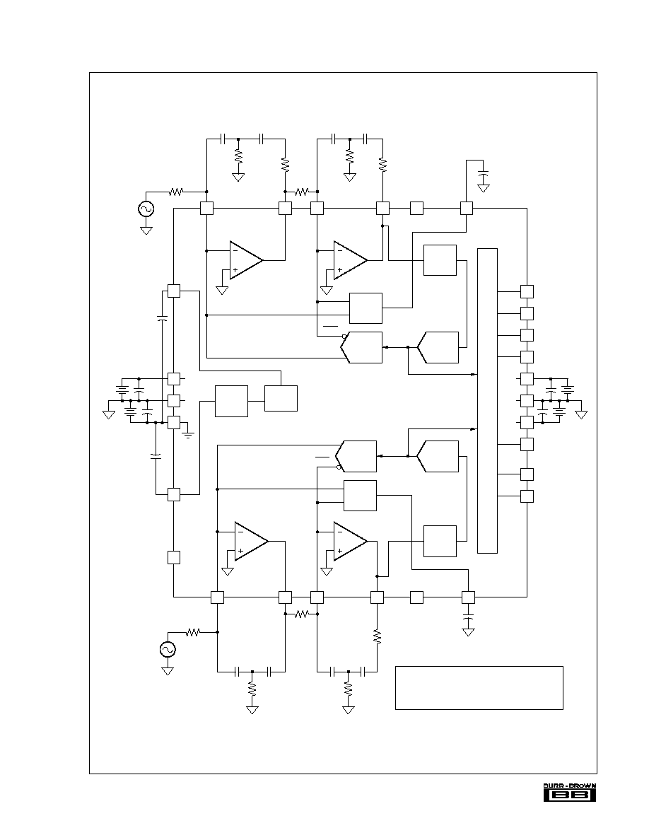
BLOCK DIAGRAM OF PCM1760
+V
CC
4
C
2
R
R
T
1R
R
IN
2R
C
1
R
R
IN
1R
C
4
R
R
Z
1R
R
T
2R
C
3
R
C
2
L
R
T
1L
R
IN
2L
C
1
L
C
4
L
R
T
2L
C
3
L
R
IN
1L
R
Z
1L
3
2
1
28
27
+
11
12
13
14
15
16
+
NC
In-1L
In-2L
Out-1L
Out-2L
NC
BPODC-L
In-1R
In-2R
Out-2R
BPODC-R
1R
2R
1L
2L
RCH
S/H
LCH
S/H
S/H
IN
L
LCH
BPO
RCH
BPO
S/H
IN
R
RCH
DAC
RCH
ADC
LCH
DAC
LCH
ADC
I
OUT
L
I
OUT
L
I
OUT
R
I
OUT
R
Band Gap
Bias
Servo
Amp
21
DGND
+
+
20
22
23
24
25
26
19
18
17
+V
DD
D
0
D
1
D
2
D
3
≠V
DD
256fs
Strobe
L/R CK
+5V
≠5V
D
e
c
o
d
e
r
T
i
m
i
n
g
C
T
L
AGND
≠V
CC
+
+
+5V
≠5V
7
8
6
Sub
SERVO
DC
5
+
+
BGDC
9
NC
10
External Components Condition
R
IN
1R/L
2.2k
C
1
, C
2
R/L
2200pF
R
TI
R/L
470
R
IN
2R/L
1.3k
C
3
, C
4
R/L
1800pF
R
T
2 R/L
560
R
Z
1 R/L
1.2k
RCH,
V
IN
Out-1R
LCH,
V
IN