DIR1703
SLES007≠ JULY 2001
DIGITAL AUDIO INTERFACE RECEIVER
1
www.ti.com
FEATURES
D
Standard Digital Audio Interface Receiver
(EIAJ1201)
D
Sampling Rate: 32 / 44.1 / 48 / 88.2 / 96 kHz
D
Recover 128 / 256 / 384 / 512 f
s
System Clock
D
Very Low Jitter System Clock Output (75 ps
Typically)
D
On-Chip Master Clock Oscillator, Only an
External Crystal Is Required:
24.576 / 22.5792 / 18.432 / 16.9344 / 16.384 /
12.288 / 11.2896 / 8.192 / 6.144 / 5.6448 /
4.096 MHz Crystals Are Available
D
Selectable Output PCM Audio Data Format
D
Selectable Crystal Clock and PPL Clock
Operation Mode
D
Output User Bit Data, Flag Signals, and
Channel Status Data With Block Start Signal
D
Single 3.3-V Power Supply
D
Package: 28 SSOP
APPLICATIONS
D
AV Receiver
D
MD Player
D
DAC Unit
DESCRIPTION
The DIR1703 is a digital audio interface receiver
(DIR) which receives and decodes audio data up
to 96 kHz according to the AES/EBU, IEC958,
S/PDIF, and EIAJCP340/1201 consumer and
professional format interface standards. The
DIR1703 demultiplexes the channel status bit and
user bit directly to serial output pins, and has
dedicated output pins for the most important
channel status bits. It also includes extensive
errors reporting.
The significant advantages of the DIR1703 are
96-kHz sampling rate capability and Low-jitter
clock recovery by the Sampling Period Adaptive
Controlled Tracking (SpAct
) system. The input
signal is reclocked with the patented Sampling
period Adaptive controlled tracking system for
maximum quality. These features are required for
recent consumer and professional audio
instruments, in which the DIR has an interface to
any kind of delta-sigma type ADC/DAC with a
96-kHz sampling rate.
This integrated circuit can be damaged by ESD. Burr-Brown recommends that all integrated circuits be handled with appropriate
precautions. Failure to observe proper handling and installation procedures can cause damage.
ESD damage can range from subtle performance degradation to complete device failure. Precision integrated circuits may be more
susceptible to damage because very small parametric changes could cause the device not to meet its published specifications.
Please be aware that an important notice concerning availability, standard warranty, and use in critical applications of
Texas Instruments semiconductor products and disclaimers thereto appears at the end of this data sheet.
PRODUCTION DATA information is current as of publication date.
Products conform to specifications per the terms of Texas Instruments
standard warranty. Production processing does not necessarily include
testing of all parameters.
Copyright
2001, Texas Instruments Incorporated
SpAct and Burr-Brown are trademarks of Texas Instruments.

DIR1703
SLES007≠ JULY 2001
2
www.ti.com
1
2
3
4
5
6
7
8
9
10
11
12
13
14
28
27
26
25
24
23
22
21
20
19
18
17
16
15
ADFLG
BRATE0
BRATE1
SCKO
V
DD
DGND
XTO
XTI
CKTRNS
LRCKO
BCKO
DOUT
SCF0
SCF1
CKSEL
UNLOCK
FMT1
FMT0
V
CC
AGND
FILT
RST
DIN
BRSEL
BFRAME
EMFLG
URBIT
CSBIT
DIR1703
(TOP VIEW)
PACKAGE/ORDERING INFORMATION
PRODUCT
PACKAGE
PACKAGE
DRAWING
NUMBER
OPERATION
TEMPERATURE
RANGE
PACKAGE
MARKING
ORDERING
NUMBER
}
TRANSPORT
MEDIA
DIR1703E
SSOP 28
324
25
∞
C to 85
∞
C
DIR1703E
DIR1703E
Rails
DIR1703E
SSOP≠28
324
≠25
∞
C to +85
∞
C
DIR1703E
DIR1703E/2K
Tape and Reel
TI equivalent no. 4040065.
Models with a slash (/) are available only in tape and reel in the quantities indicated (e.g., /2K indicates 2000 devices per reel). Ordering 2000
pieces of DIR1703E/2K will get a single 2000-piece tape and reel.
block diagram
OSC
OSC
Selector
PLL1
PLL2
SpAct
FIFO
SCKO
BRSEL
CKSEL
BCKO
LRCKO
DOUT
BFRAME
URBIT
CSBIT
ADFLG
EMFLG
SCF
FMT
DGND
AGND
2
XTI
RST
Audio Clock
And Data
Generator
XTO
DIN
BRATE
UNLOCK CKTRNS
FILT
100 MHZ
wrclk
rdclk
VDD
S/PDIF
Decoder
VCC

DIR1703
SLES007≠ JULY 2001
3
www.ti.com
Terminal Functions
TERMINAL
I/O
DESCRIPTIONS
NAME
PIN
I/O
DESCRIPTIONS
ADFLG
1
O
Audio data or digital data flag
BRATE0
2
O
fs rate flag 0 (32 k, 44.1 k, 48 k, and 88 k / 96 k)
BRATE1
3
O
fs rate flag 1 (32 k, 44.1 k, 48 k, and 88 k / 96 k)
SCKO
4
O
System clock output
VDD
5
≠
Digital power supply, +3.3 V
DGND
6
≠
Digital ground
XTO
7
O
Crystal oscillator output
XTI
8
I
Crystal oscillator input, external clock input
CKTRNS
9
O
Clock transition status output
LRCKO
10
O
Audio latch enable (LRCK, fs) output
BCKO
11
O
Audio bit clock output
DOUT
12
O
Audio serial data output
SCF0
13
I
System clock frequency select (128/256/384/512 fs) (see Note 1)
SCF1
14
I
System clock frequency select (128/256/384/512 fs) (see Note 1)
CSBIT
15
O
Channel status bit output (see Note 2)
URBIT
16
O
User bit output (see Note 2)
EMFLG
17
O
Emphasis flag
BFRAME
18
O
Block start clock (B-frame)
BRSEL
19
I
Default bit rate select (32 / 44.1 / 48 / 88.2 / 96 kHz) (see Note 1)
DIN
20
I
S/PDIF data digital input (see Note 4)
RST
21
I
Reset input, active LOW (see Note 3)
FILT
22
≠
External filter
AGND
23
≠
Analog ground
VCC
24
≠
Analog power supply, 3.3V
FMT0
25
I
Audio data format select (see Note 1)
FMT1
26
I
Audio data format select (see Note 1)
UNLOCK
27
O
PLL unlock or parity error flag
CKSEL
28
I
System clock operation mode selected. Low: PLL, High: Crystal (see Note 1)
NOTES:
1. Schmitt trigger input with internal pulldown (TYP 51 k
), 5 V tolerant.
2. Serial outputs are utilized for both consumer and professional application.
3. Schmitt trigger input with internal pullup (TYP 51 k
), 5 V tolerant.
4. CMOS level input with internal pulldown (TYP 51 k
), 5 V tolerant.

DIR1703
SLES007≠ JULY 2001
4
www.ti.com
absolute maximum ratings
Supply voltage, V
CC
, V
DD
4.0 V
. . . . . . . . . . . . . . . . . . . . . . . . . . . . . . . . . . . . . . . . . . . . . . . . . . . . . . . . . . . . . . . . .
Supply voltage differences, V
CC
, V
DD
±
0.1 V
. . . . . . . . . . . . . . . . . . . . . . . . . . . . . . . . . . . . . . . . . . . . . . . . . . . . . . .
Ground voltage differences, AGND, DGND
±
0.1 V
. . . . . . . . . . . . . . . . . . . . . . . . . . . . . . . . . . . . . . . . . . . . . . . . . .
Digital input voltage:
Digital input pins except XTI
≠0.3 V to (6.5 V + 0.3 V)
. . . . . . . . . . . . . . . . . . . . . . . . . .
XTI
≠0.3 V to (V
DD
+ 0.3 V)
. . . . . . . . . . . . . . . . . . . . . . . . . . . . . . . . . . . . . . . . . . . . . . . . .
Input current (Any pins except supplies)
±
10 mA
. . . . . . . . . . . . . . . . . . . . . . . . . . . . . . . . . . . . . . . . . . . . . . . . . . . .
Ambient temperature under bias
≠40
∞
C to 125
∞
C
. . . . . . . . . . . . . . . . . . . . . . . . . . . . . . . . . . . . . . . . . . . . . . . . . . . .
Storage temperature
≠55
∞
C to 150
∞
C
. . . . . . . . . . . . . . . . . . . . . . . . . . . . . . . . . . . . . . . . . . . . . . . . . . . . . . . . . . . . .
Junction temperature
150
∞
C
. . . . . . . . . . . . . . . . . . . . . . . . . . . . . . . . . . . . . . . . . . . . . . . . . . . . . . . . . . . . . . . . . . . . .
Lead temperature (soldering)
260
∞
C, 5 sec
. . . . . . . . . . . . . . . . . . . . . . . . . . . . . . . . . . . . . . . . . . . . . . . . . . . . . . . .
Package temperature (IR reflow, peak)
235
∞
C, 10 sec
. . . . . . . . . . . . . . . . . . . . . . . . . . . . . . . . . . . . . . . . . . . . . . .
Stresses beyond those listed under "absolute maximum ratings" may cause permanent damage to the device. These are stress ratings only, and
functional operation of the device at these or any other conditions beyond those indicated under "recommended operating conditions" is not
implied. Exposure to absolute-maximum-rated conditions for extended periods may affect device reliability.

DIR1703
SLES007≠ JULY 2001
5
www.ti.com
electrical characteristics, all specifications at T
A
= 25
∞
C, V
CC
= V
DD
= 3.3 V (unless otherwise noted)
PARAMETER
TEST CONDITIONS
MIN
TYP
MAX
UNIT
DIGITAL INPUT/OUTPUT
VIH (5)
2
5.5
VIL (5)
0.8
VIH2 (6)
Input logic level
70%VDD
VDC
VIL2 (6)
Input logic level
30%VDD
VDC
VIH3 (7)
70%VDD
5.5
VIL3 (7)
30%VDD
VOH (8)
IO = 1 mA
VDD≠0.4
VOL (8)
Output logic level
IO = ≠2 mA
0.5
VDC
VOH (9)
Output logic level
IO = 2 mA
VDD≠0.4
VDC
VOL (9)
IO = ≠4 mA
0.5
IIH(10)
VIN = VDD
65
100
IIL(10)
VIN = 0 V
≠10
10
IIH(11)
Input leakage current
VIN = VDD
≠10
10
µ
A
IIL(11)
Input leakage current
VIN = 0 V
≠100
≠65
µ
A
IIH(6)
VIN = VDD
≠10
10
IIL(6)
VIN = 0 V
≠10
10
fs(12)
Input sampling frequency
32
96
kHz
SCKO
System clock frequency
4.096
128/256/
384/512 fs
49.152
MHz
tj
SCKO clock jitter
75
ps RMS
SCKO duty cycle
50%
XTI clock accuracy
≠500
See
Table 3
500
ppm
S/PDIF INPUT
Duty cycle
VIN = 1.5 V, fs = 96 kHz
15%
85%
Jitter
VIN = 1.5 V
±
10
ns p-p
POWER SUPPLY REQUIREMENTS
VDD, VCC
Voltage range
3
3.3
3.6
VDC
ICC (VCC)
Supply current (see Note 13)
3.4
4.7
mA
IDD (VDD)
Supply current (see Note 13)
26
36
mA
PD
Power dissipation
100
mW
TEMPERATURE RANGE
Operation temperature
≠25
85
∞
C
JA
Thermal resistance
28-pin SSOP
100
∞
C/W
NOTES:
5. TTL compatible, except pins 8, 20: XTI, DIN.
6. Pin 8: XTI (CMOS logic level).
7. Pin 20: DIN (CMOS logic level).
8. Pins 1
≠
3, 9, 17
≠
18, 27: ADFLG, BRATE0, BRATE1, CKTRNS, EMFLG, BFRAME, UNLOCK.
9. Pins 4, 10
≠
12, 15
≠
16: SCKO, LRCKO, BCKO, DOUT, CSBIT, URBIT.
10. Pins 13
≠
14, 19
≠
20, 25
≠
26, 28: SCF0, SCF1, BRSEL, DIN, FMT0, FMT1, CKSEL.
11. Pin 21: RST
12. fs is defined as the incoming audio sampling frequency per channel.
13. No load connected to SCKO, LRCKO, BCKO, DOUT, CSBIT, URBIT. Power supply current varies according to the system clock
frequency.

DIR1703
SLES007≠ JULY 2001
6
www.ti.com
basic operation theory
The DIR1703 is operated as either a PLL clock operation mode or a crystal clock operation mode. These basic
operation modes are user selectable.
Sampling period adaptive controlled tracking system (SpAct) is a newly developed clock recover architecture,
giving very low jitter clock from S/PDIF data input.
The DIR1703 has two PLLs, PLL1 and PLL2. SpAct is supplied with a 100 MHz executing clock from PLL1.
The DIR1703 requires system clock input for operation of SpAct at both the PLL clock operation mode and the
crystal clock operation mode. This system clock can be obtained by connecting a crystal resonator at the
XTI/XTO pins or applying an external clock input at the XTI pin as shown in Figure 1.
PLL2 generates the system clock SCKO by using the output signal of the SpAct. The source of SCKO, either
OSC (crystal) or PLL2, is selected by the CKSEL pin (called PLL clock operation mode and crystal clock
operation mode).
In the PLL clock operation mode, when the S/PDIF signal goes to noninput, SCKO may hold the latest tracked
frequency.
Also, the DIR1703 indicates the unlocked state by a high level output at the UNLOCK pin. When the S/PDIF
signal restarts, the analog PLL will lock to the incoming S/PDIF signal with very low jitter. The PLL lock-in time
is around 1 ms using the SpAct.
Then, the DIR1703 indicates the locked status by a low output at the UNLOCK pin. In this status, the BRATE
pins simultaneously indicate the bit rate of the incoming S/PDIF signal.
After RST
(pin 21) is removed, SCKO is set to the default frequency, which can be selected by the BRSEL and
SCF pins. The sampling rate (f
S
), 32 k, 44.1 k, 48 k, 88.2 k, or 96 k is selected by the BRSEL pin. The system
clock frequency, 128, 256, 384, or 512 f
S
is also selected by the SCF pins.
In the crystal clock operation mode, the crystal oscillator generates three audio clocks SCKO, BCKO, and
LRCKO. In this mode, DOUT is always set to mute (zero). BRATE and UNLOCK can be indicated according
to the incoming S/PDIF signal.
If CKSEL (pin 28) is connected to UNLOCK (pin 27), which indicates the S/PDIF decoding status and the PLL2
lock-state, the system clock source can be selected automatically when the S/PDIF signal is active and the bit
rate is detected.
Crystal
C 1
DIR1703
XTO
XTI
Open
DIR1703
XTO
XTI
C2
R1 = 1 M
,
C1, C2 = 10 TO 33 pF
XTAL
OSC
CIR
XTAL
OSC
CIR
External Clock
R1
Crystal Resonator Connection
External Clock Input
Figure 1. System Clock Connections

DIR1703
SLES007≠ JULY 2001
7
www.ti.com
system clock output
The primary function of the DIR1703 is to recover audio data and a low jitter clock from a digital audio
transmission line. The system clock (SCKO) can be selected in two clocks that are generated by the crystal
oscillator clock (crystal mode) or the PLL clock (PLL mode) by the SpAct.
The two operation modes are selected by the CKSEL pin. In the PLL clock operation mode, the clock that can
be generated is SCKO (128 / 256 / 384 / 512 f
S
, shown in Table 1), BCKO (64 f
S
), and LRCKO (1 f
S
). SCKO
is the output of the voltage controlled oscillator (VCO) in an analog PLL. The PLL function consists of a VCO,
phase and frequency detector, and a external second-order loop filter. The closed-loop transfer function, which
specifies the PLL jitter attenuation characteristics, is shown in Figure 2. In the crystal clock operation mode,
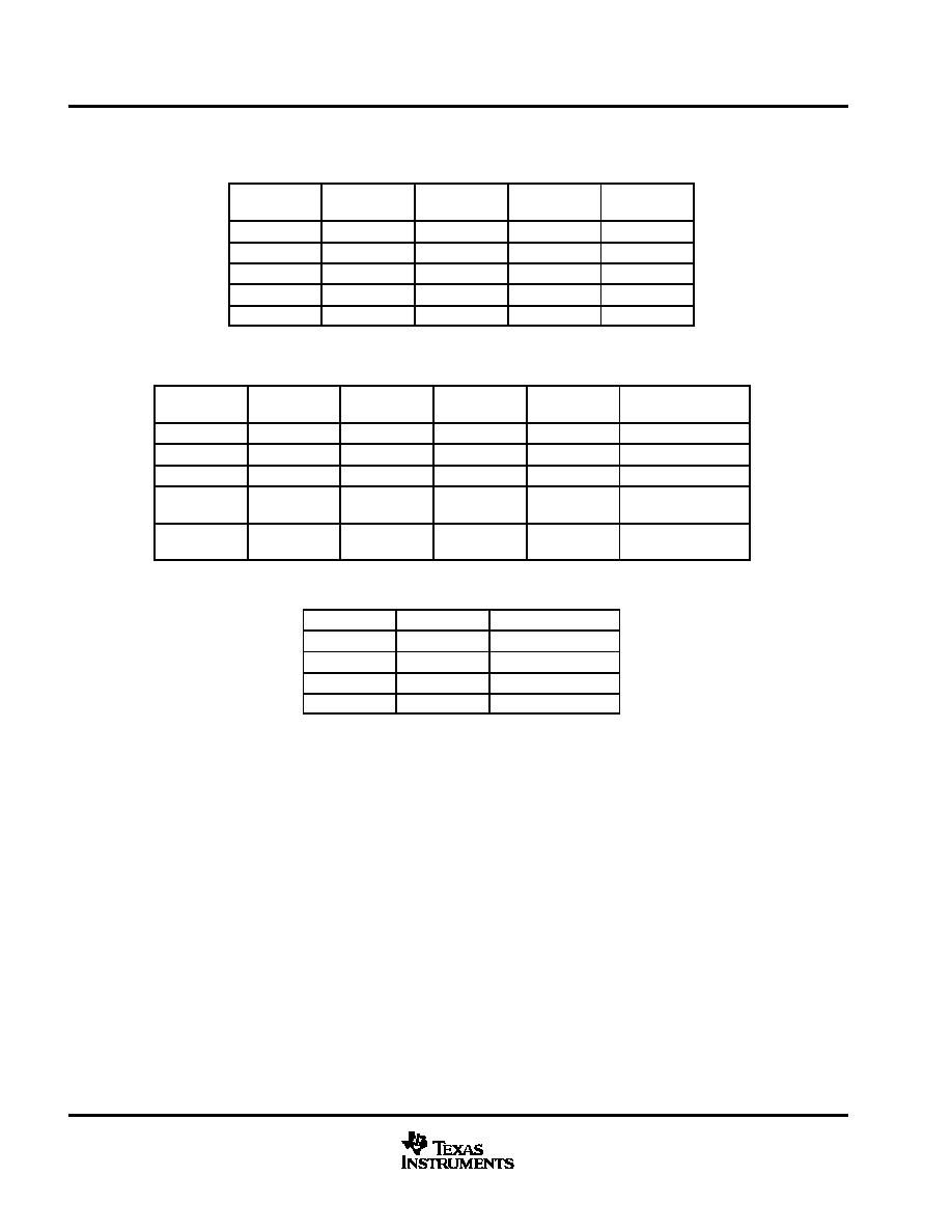
SCKO can be generated from several crystal oscillators shown in Table 2.
The crystal frequency should be defined for internal PLL by connecting the BRSEL pin to one of the output pins
BFRAME, EMFLG, URBIT, or CSBIT as shown in Table 3. A 12.288 MHz crystal resonator can be used for
96-kHz ≠ 128 f
S
(CSBIT), 48-kHz ≠ 256 f
S
(OPEN) and 32-kHz ≠ 384 f
S
(BFRAME). If BRSEL is not connected
to any pins, the 48-kHz sampling rate is selected. The system clock frequency of both modes can be selected
by control data at SCF0 and SCF1 pins shown in Table 4.
Table 5 shows the state of the system and the condition of audio clocks and flags in both the PLL and crystal
operation modes. In the crystal clock operation mode, SpAct also detects the bit rate of the incoming S/PDIF
signal and indicates the state at the UNLOCK pin. Therefore, by connecting CKSEL pin 28) to UNLOCK (pin
27), the system clock source can be selected automatically when the S/PDIF signal arrives and the bit rate is
detected. The required accuracy for clock frequency of the crystal resonator or external clock input is
±
500 ppm.
Table 1. Generated System Clock (SCKO) PLL Clock Operation Mode
SAMPLING
RATE
128 fS
256 fS
384 fS
512 fS
32 kHz
yes
yes
yes
yes
44.1 kHz
yes
yes
yes
yes
48 kHz
yes
yes
yes
yes
88.2 kHz
yes
yes
yes
yes
96 kHz
yes
yes
yes
yes
≠100
≠80
≠60
≠40
≠20
0
100
10 k
1 M
100 M
Closed Loop Gain
≠
dB
f ≠ Frequency ≠ kHz
1 k
100 k
10 M
Figure 2. Jitter Attenuator Characteristics With Specified Loop Filter
DIR1703
SLES007≠ JULY 2001
8
www.ti.com
system clock output (continued)
Table 2. Generated System Clock (SCKO) Crystal Clock Operation Mode
SAMPLING
RATE
128 fS
256 fS
384 fS
512 fS
32 kHz
yes
yes
yes
yes
44.1 kHz
yes
yes
yes
yes
48 kHz
yes
yes
yes
yes
88.2 kHz
yes
yes
yes
yes
96 kHz
yes
yes
See Note 14
See Note 14
NOTE 14: External clock only
Table 3. Selectable Crystal Oscillator
SAMPLING
RATE
128 fS
256 fS
384 fS
512 fS
BRSEL
CONNECTED TO
32 kHz
4.096 MHz
8.192 MHz
12.288 MHz
16.384 MHz
BFRAME
44.1 kHz
5.6448 MHz
11.2896 MHz
16.9344 MHz
22.5792 MHz
EMFLG
48 kHz
6.144 MHz
12.288 MHz
18.432 MHz
24.576 MHz
open
88.2kHz
11.2896 MHz
22.5792 MHz
33.8688 MHz
(see Note 14)
45.1584 MHz
(see Note 14)
URBIT
96 kHz
12.288 MHz
24.576 MHz
36.864 MHz
(see Note 14)
49.152 MHz
(see Note 14)
CSBIT
Table 4. System Clock Selection
SCF1
SCF0
SYSTEM CLOCK
LOW
LOW
128 fS
LOW
HIGH
256 fS
HIGH
LOW
384 fS
HIGH
HIGH
512 fS

DIR1703
SLES007≠ JULY 2001
9
www.ti.com
system clock output (continued)
Table 5. System Clock Operation Mode
CONDITIONS
CLOCK AND DATA OUTPUTS
MODE
CKSEL
S/PDIF
DATA
SCKO
BCKO
LRCKO
DOUT
BRATE
UNLOCK
CS. UR
BIT
AD.
EMFLG
After
RESET
Default PLL
(128, 256, 384, 512
fS)
Default
PLL
(64 fS)
Default
PLL
(1 fS)
MUTE
LOW
HIGH
LOW
LOW
PLL
LOW
YES
PLL
(128, 256, 384, 512
fS)
PLL
(64 fS)
PLL
(1 fS)
DATA
DETECT
LOW
DATA
DATA
NO
HOLD
(128, 256, 384, 512
fS)
HOLD
(64 fS)
HOLD
(1 fS)
MUTE
HOLD
HIGH
Unknown
HOLD
After
RESET
Crystal
(128, 256, 384, 512
fS)
Crystal
(64 fS)
Crystal
(1 fS)
MUTE
LOW
HIGH
LOW
LOW
CRYSTAL
HIGH
YES
Crystal
(128, 256, 384, 512
fS)
Crystal
(64 fS)
Crystal
(1 fS)
MUTE
DETECT
LOW
Unknown
LOW
NO
Crystal
(128, 256, 384, 512
fS)
Crystal
(64 fS)
Crystal
(1 fS)
MUTE
Unknown
HIGH
Unknown
LOW
In the PLL mode, the DIR1703 will be the same frequencies as the crystal mode after RESET; however, the frequency error is below 1%.
Holds the latest tracked frequency.
SCKO timing
L
H
0.8 V
2 V
System Clock Pulse
Cycle Time
tSCKH
tSCKL
SCKO
SCKO Clock Pulse Width High
tSCKH
7 ns (min)
SCKO Clock Pulse Width Low
tSCKL
7 ns (min)
1/128 fS, 1/256 fS, 1/384 fS or 1/512 fS.

DIR1703
SLES007≠ JULY 2001
10
www.ti.com
bit rate detection
By using the SpAct frequency estimator (not the S/PDIF channel status bit), the DIR1703 automatically detects
the sample rate of an incoming S/PDIF signal and indicates the frequency at the BRATE pins.
Table 6 lists the frequency ranges reported. Except for 88.2 and 96 kHz, these sample rates are the same as
the channel status bit defined in the S/PDIF specifications. When the bit-rate is 88.2 or 96 kHz the indicator
shows the same HL value. This state is not defined in the S/PDIF specifications.
Table 6. Incoming Sample Frequency Bits
SAMPLING RATE
BRATE1
BRATE0
32 kHz
HIGH
HIGH
44.1 kHz
LOW
LOW
48 kHz
LOW
HIGH
88.2 kHz
HIGH
LOW
96 kHz
HIGH
LOW
timing specification for PLL operation
lock-up time
Lock
L
H
tINT< 1 ms
Unlock
DIN Start
PLL
Condition
PLL Status
Indicator Pin
Site UNLOCK
Figure 3. PLL Lock Up Timing
relation between audio-data-output timing and PLL condition indicator timing
In the PLL clock operation mode, when the S/PDIF signal is not detected after reset removal, audio clocks
(SCKO, BCKO, LRCKO) which are not related to S/PDIF signal are generated by SpAct. The bit rate can be
selected by setting pin BRSEL. If BRSEL is OPEN or connected to DGND, the default bit rate frequency is set
to 48 kHz. If BRSEL is connected to one of the output pins BFRAME, EMFLG, URBIT, or CSBIT, the frequency
is set to 32, 44.1, 88.2, or 96 kHz, respectively. Therefore, the initial frequency is the same as the crystal
resonator, however, its error frequency is below 1% after reset.
When the analog PLL is still unlocked after at least ten rising-edges of the S/PDIF, a S/PDIF decoder can detect
the incoming S/PDIF signal. Thus, DOUT becomes low (MUTE) until the analog PLL locks. This MUTE period
is less than 1 ms (analog PLL's lock-up time is less than 0.5 ms). When the decoder does not detect an incoming
S/PDIF signal, UNLOCK will output high level status at the LRCKO clock transition. SCKO keeps its frequency
at the latest tracked bit rate.

DIR1703
SLES007≠ JULY 2001
11
www.ti.com
relation between audio-data-output timing and PLL condition indicator timing (continued)
2
1
Mute
L
H
31
32
Mute
Unlock
Lock
PLL
Condition
UNLOCK
LRCKO
BCKO
DOUT
Figure 4. Relation Between Audio Data Output Timing and UNLOCK Flag Timing
unlock flag minimum pulse width time
CASE-A when PLL is unlocked
In the PLL clock operation mode, when PLL goes to unlock by a disconnected S/PDIF signal, the UNLOCK flag
pin indicates high and the audio data output DOUT becomes low (MUTE). The MUTE period, t
(UNL)
, is a
minimum of 200 ms. In this period, SCKO, BCKO, and LRCKO frequencies hold the latest tracked frequency.
If the S/PDIF signal is connected again in this unlock period, the bit rate is changed to the incoming signal
frequency, after at least 1 ms (before the UNLOCK flag becomes low). CKTRNS indicates the validity of SCKO.
When CKTRNS is high, the frequency of SCKO, BCKO, and LRCKO is in transition.

DIR1703
SLES007≠ JULY 2001
12
www.ti.com
2
1
L
H
Mute
t(UNL)>200 ms
S/PDIF Signal Bit Rate
S/PDIF Signal Starts Again
New Bit Rate
t(TRNS) < 1 ms
UNLOCK
LRCKO
CKTRANS
BCKO
DOUT
Figure 5. UNLOCK Flag Minimum Pulse Width Time for PLL Unlocked
CASE-B when parity error occurs
When a parity error occurs in one subframe interval, UNLOCK becomes high during this subframe, then returns
low at the next arriving subframe.
During this subframe with parity error, the data output will hold the previous data of each channel.
H
L
Same as The Previous Data
24
1
24
1
2
UNLOCK
LRCKO
BCKO
DOUT
CASE-B When Parity Error Occurs
Figure 6. UNLOCK Timing for Parity Error

DIR1703
SLES007≠ JULY 2001
13
www.ti.com
PCM audio interface
The DIR1703 can produce 16-bit or 24-bit output data in standard format and 24-bit output data in IIS format.
The PCM audio interface format of the DIR1703 is selected using the format pins FMT1, FMT0. Table 7 shows
the FMT pin configuration.
Table 7. Audio Output Data Format Select
FMT1
FMT0
AUDIO DATA FORMAT
LOW
LOW
16 bit MSB first, Right justified
LOW
HIGH
24 bit MSB first, Right justified
HIGH
LOW
24 bit MSB first, Left justified
HIGH
HIGH
24 bit IIS
22 23 24
14 15 16
MSB
2
1
LSB
15 16
MSB
2
1
LSB
23 24
MSB
2
1
LSB
23 24
MSB
2
1
LSB
15 16
MSB
2
1
LSB
23 2 4
MSB
2
1
LSB
23 24
1
MSB
2
1
LSB
23 24
MSB
2
1
LSB
23 24
1/fS
L≠Channel
R≠Channel
LRCKO
BCKO
Right Justified
Audio Data Word = 16≠Bit
Right Justified
Audio Data Word = 24≠Bit
Left Justified
Audio Data Word = 24≠Bit
LRCKO
BCKO
Audio Data Word = 24≠Bit
DOUT
DOUT
DOUT
DOUT
1/fS
L≠Channel
R≠Channel
Standard Data Format; L≠Channel = HIGH, R≠Channel = LOW
IIS Data Format; L≠Channel = LOW, R≠Channel = HIGH
Figure 7. Audio Data Output Format

DIR1703
SLES007≠ JULY 2001
14
www.ti.com
PCM audio interface (continued)
50% of VDD
50% of VDD
50% of VDD
50% of VDD
t(SL)
t(LS)
t(BCH)
t(BCL)
t(LB)
t(BL)
t(BCY)
t(DS)
t(DH)
SCKO
LRCKO
BCKO
DOUT
PARAMETERS
MIN
MAX
UNITS
t(SL)
SCKO rising edge to LRCKO edge
11
ns
t(LS)
LRCKO edge to SCKO rising edge
5
ns
t(BCY)
BCKO pulse cycle time
64 fS
t(BCL)
BCKO pulse width low
78
ns
t(BCH)
BCKO pulse width high
78
ns
t(BL)
BCKO rising edge to LRCKO edge
78
ns
t(LB)
LRCKO edge to BCKO rising edge
78
ns
t(DS)
DOUT setup time
78
ns
t(DH)
DOUT hold time
78
ns
Figure 8. Audio Data Output Timing
dedicated output pins for both professional and consumer applications
The DIR1703 has parallel output pins for both professional and consumer applications. In the professional mode
de-emphasis flag EMFLG indicates a 50/15-
µ
s time constant pre-emphasis. Professional mode is set when Bit
0 of CSBIT Byte 0 is high. When Bits 2 to 4 of CSBIT Byte 0 is 110, the EMFLG becomes high. In other cases,
EMFLG is low. Audio/non-audio flag ADFLG indicates S/PDIF data mode, i.e., Bit 1 of CSBIT Byte 0. When
ADFLG is low, S/PDIF data includes PCM audio signal. In other cases, ADFLG is high.
In the consumer mode EMFLG indicates 2-channel audio with a 50/15-
µ
s time constant pre-emphasis.
Consumer mode is set when Bit 0 of CSBIT Byte 0 is low. When Bits 3 to 5 of CSBIT Byte 0 is 100, EMFLG
becomes high. In other cases, EMFLG is low. The ADFLG signal indicates whether S/PDIF includes digital data,
such as AC-3 or not. When Bit 1 of CSBIT Byte 0 is high, the incoming S/PDIF includes a non-audio signal. In
other cases, ADFLG is low.
These dedicated output pins are checked for only L-ch CS information. The DIR1703 does not support CRC
check function in the professional mode. As for other flags, CS bit and user-bit for professional and consumer
applications, are directly supplied by serial mode at CSBIT (pin 15) and URBIT (pin 16). These pins indicate
L-ch and R-ch information sequentially.

DIR1703
SLES007≠ JULY 2001
15
www.ti.com
dedicated output pins for both professional and consumer applications (continued)
Audio data and clock timing are described below. The serial output data starts after 16
±
8 BCKO clocks from
when the corresponding subframe arrives. When B subframe arrives, the BFRAME pin becomes high during
1/f
s
x 32 (s), then BFRAME returns to low after 32 frames.
S/PDIF
URBIT/CSBIT/UNLOCK etc.
LRCKO
BFRAME
LRCKO
Frame 0
Frame 1
B
W
M
W
M
W
B
Frame 191
Frame 0
L191
R191
L0
R0
L1
R1
64 1
2
3
BCKO
DOUT
1/fS (S)
1/fS x 32 (S)
1/fS x 192 (S)
16
±
8 BCKO Delay
64 BCKO
Figure 9. Timing Chart for Audio Data and Channel Status

DIR1703
SLES007≠ JULY 2001
16
www.ti.com
reset sequence
The DIR1703 requires external reset operation after power on. Figure 10 shows the reset sequence after power
on. The DIR1703 is ready for receiving S/PDIF signal when the internal reset sequence has finished and
CKTRNS goes to LOW. BFRAME, EMFLG, URBIT and CSBIT pins are used for configuration during the period
from the rising edge of RST to the falling edge of CKTRNS. S/PDIF signal is accepted after CKTRNS goes to
LOW. The minimum pulse width of RST, t
RST
is 100 ns. The RST delay after the power supply reaches 3 V should
be at least 10 ms. All of the output pins except CKTRNS and UNLOCK are LOW during RST LOW.
LOW
HIGH
LOW
HIGH
HIGH
Chip Status Information
LOW
Unstable
Stable
3 V
VDD, VCC
XTI
XTO
RST
BFRAME,
EMFLG,
VRBIT,
CSBIT
CKTRNS
DIN
UNLOCK
DIR1703 Ready
Internal PLL ON
tSTT > 10 ms
tRST > 100 ns
12.5XTI Clock
Unknown
Valid
1160XTI Clock
< 5 fs
S/PDIF Acceptable
< 1 ms
NOTE: SCF0 and SCF1 should be settled during RST assertion. The change of SCF0 and SCF1 is not permitted during normal operation. When
the change is needed, the reset sequence must be started by asserting RST again.
Figure 10. After Power ON

DIR1703
SLES007≠ JULY 2001
17
www.ti.com
typical circuit connection
ADFLG
BRATE0
BRATE1
SCKO
VDD
DGND
XTO
XTI
CKTRNS
LRCKO
BCKO
DOUT
SCF0
SCF1
CKSEL
UNLOCK
FMT1
FMT0
VCC
AGND
FILT
RST
DIN
BRSEL
BFRAME
EMFLG
URBIT
CSBIT
1
2
3
4
5
6
7
8
9
10
11
12
13
14
28
27
26
25
24
23
22
21
20
19
18
17
16
15
C7
C8
R2
C2
3.3 V VCC
C4
Data Format Select
Reset (Active LOW)
Receiver Circuit
BRSEL Connection Depends Upon
Crystal Resonator Frequency.
Audio Data
Processor
System Clock
Frequency Select
(128,256,348, 512 fs)
C6
R1
C5
C1
C3
3.3 V VDD
Bit Rate Indicator
C1 , C2: Bypass Capacitor, 1
µ
F to 10
µ
F
C3 , C4: Bypass Capacitor, 0.01
µ
F to 0.1
µ
F
C5 , C6: OSC Capacitor, 10 to 33 pF
C7:
Loop Filter Capacitor, 0.068
µ
F
C8:
Loop Filter Capacitor, 0.0082
µ
F
R1:
OSC Resistor, 1 M
R2:
Loop Filter Resistor, 1.2 k
+
+
For Automatic System Clock Selection

DIR1703
SLES007≠ JULY 2001
18
www.ti.com
DB (R-PDSO-G**)
PLASTIC SMALL-OUTLINE
4040065/D 09/00
28 PINS SHOWN
Gage Plane
8,20
7,40
0,15 NOM
0,55
0,95
0,25
38
12,90
12,30
28
10,50
24
8,50
Seating Plane
9,90
7,90
30
10,50
9,90
0,38
5,60
5,00
15
0,22
14
A
28
1
20
16
6,50
6,50
14
0,05 MIN
5,90
5,90
DIM
A MAX
A MIN
PINS **
2,00 MAX
6,90
7,50
0,65
M
0,15
0
∞
≠8
∞
0,10
NOTES: A. All linear dimensions are in millimeters.
B. This drawing is subject to change without notice.
C. Body dimensions do not include mold flash or protrusion not to exceed 0,15.
D. Falls within JEDEC MO-150

IMPORTANT NOTICE
Texas Instruments and its subsidiaries (TI) reserve the right to make changes to their products or to discontinue
any product or service without notice, and advise customers to obtain the latest version of relevant information
to verify, before placing orders, that information being relied on is current and complete. All products are sold
subject to the terms and conditions of sale supplied at the time of order acknowledgment, including those
pertaining to warranty, patent infringement, and limitation of liability.
TI warrants performance of its products to the specifications applicable at the time of sale in accordance with
TI's standard warranty. Testing and other quality control techniques are utilized to the extent TI deems necessary
to support this warranty. Specific testing of all parameters of each device is not necessarily performed, except
those mandated by government requirements.
Customers are responsible for their applications using TI components.
In order to minimize risks associated with the customer's applications, adequate design and operating
safeguards must be provided by the customer to minimize inherent or procedural hazards.
TI assumes no liability for applications assistance or customer product design. TI does not warrant or represent
that any license, either express or implied, is granted under any patent right, copyright, mask work right, or other
intellectual property right of TI covering or relating to any combination, machine, or process in which such
products or services might be or are used. TI's publication of information regarding any third party's products
or services does not constitute TI's approval, license, warranty or endorsement thereof.
Reproduction of information in TI data books or data sheets is permissible only if reproduction is without
alteration and is accompanied by all associated warranties, conditions, limitations and notices. Representation
or reproduction of this information with alteration voids all warranties provided for an associated TI product or
service, is an unfair and deceptive business practice, and TI is not responsible nor liable for any such use.
Resale of TI's products or services with
statements different from or beyond the parameters stated by TI for
that product or service voids all express and any implied warranties for the associated TI product or service,
is an unfair and deceptive business practice, and TI is not responsible nor liable for any such use.
Also see: Standard Terms and Conditions of Sale for Semiconductor Products. www.ti.com/sc/docs/stdterms.htm
Mailing Address:
Texas Instruments
Post Office Box 655303
Dallas, Texas 75265
Copyright
2001, Texas Instruments Incorporated