 | –≠–ª–µ–∫—Ç—Ä–æ–Ω–Ω—ã–π –∫–æ–º–ø–æ–Ω–µ–Ω—Ç: HCPL4502 | –°–∫–∞—á–∞—Ç—å:  PDF PDF  ZIP ZIP |
6N135, 6N136, HCPL4502
OPTOCOUPLERS/OPTOISOLATORS
SOES022A ≠ JULY 1986 ≠ REVISED APRIL 1998
1
POST OFFICE BOX 655303
∑
DALLAS, TEXAS 75265
D
Compatible with TTL Inputs
D
High-Speed Switching . . . 1 Mbit/s Typ
D
Bandwidth . . . 2 MHz Typ
D
High Common-Mode Transient
Immunity . . . 1000 V/
µ
s Typ
D
High-Voltage Electrical
Insulation . . . 3000 Vdc Min
D
Open-Collector Output
D
UL Recognized . . . File Number 65085
description
These high-speed optocouplers are designed for use in analog or digital interface applications that require
high-voltage isolation between the input and output. Applications include line receivers that require high
common-mode transient immunity, and analog or logic circuits that require input-to-output electrical isolation.
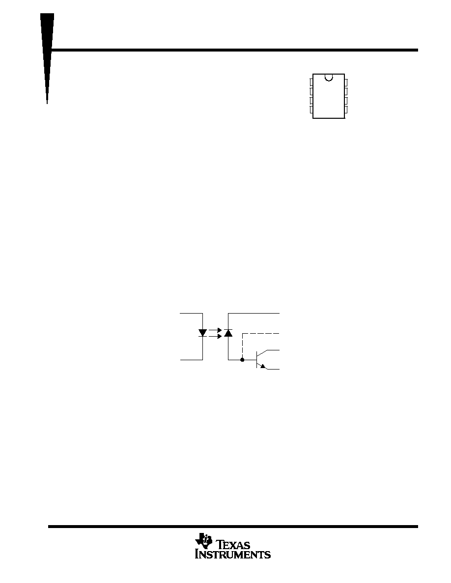
The 6N135, 6N136, and HCPL4502 optocouplers each consists of a light-emitting diode and an integrated
photon detector composed of a photodiode and an open-collector output transistor. Separate connections are
provided for the photodiode bias and the transistor-collector output. This feature, which reduces the transistor
base-to-collector capacitance, results in speeds up to one hundred times that of a conventional phototransistor
optocoupler.
The 6N135 is designed for TTL/CMOS, TTL/LSTTL, and wide-band analog applications.
The 6N136 and HCPL4502 are designed for high-speed TTL/TTL applications. The HCPL4502 has no base
connection.
schematic
VCC
BASE: 6N135, 6N136
OPEN: HCPL4502
OUTPUT
GND
8
7
6
5
2
3
ANODE
CATHODE
Copyright
©
1998, Texas Instruments Incorporated
PRODUCTION DATA information is current as of publication date.
Products conform to specifications per the terms of Texas Instruments
standard warranty. Production processing does not necessarily include
testing of all parameters.
1
2
3
4
8
7
6
5
NC
ANODE
CATHODE
NC
V
CC
BASE/OPEN
OUTPUT
GND
6N135, 6N136, OR HCPL4502 PACKAGE
(TOP VIEW)
Terminal 7 is BASE on the 6N135 and
6N136 and OPEN on the HCPL4502
NC ≠ No internal connection

6N135, 6N136, HCPL4502
OPTOCOUPLERS/OPTOISOLATORS
SOES022A ≠ JULY 1986 ≠ REVISED APRIL 1998
2
POST OFFICE BOX 655303
∑
DALLAS, TEXAS 75265
absolute maximum ratings at 25
∞
C free-air temperature (unless otherwise noted)
Supply and output voltage range, V
CC and
V
O
≠ 0.5 V to 15 V
. . . . . . . . . . . . . . . . . . . . . . . . . . . . . . . . . . . . . . . .
Reverse input voltage
5 V
. . . . . . . . . . . . . . . . . . . . . . . . . . . . . . . . . . . . . . . . . . . . . . . . . . . . . . . . . . . . . . . . . . . . . . .
Emitter-base reverse voltage
5 V
. . . . . . . . . . . . . . . . . . . . . . . . . . . . . . . . . . . . . . . . . . . . . . . . . . . . . . . . . . . . . . . . .
Peak input forward current (pulse duration = 1 ms, 50% duty cycle, see Note 1)
50 mA
. . . . . . . . . . . . . . . . . .
Peak transient input forward current (pulse duration 1
µ
s, 300 Hz)
1 A
. . . . . . . . . . . . . . . . . . . . . . . . . . . . . . . . .
Average forward input current(see Note 2)
25 mA
. . . . . . . . . . . . . . . . . . . . . . . . . . . . . . . . . . . . . . . . . . . . . . . . . .
Peak output current
16 mA
. . . . . . . . . . . . . . . . . . . . . . . . . . . . . . . . . . . . . . . . . . . . . . . . . . . . . . . . . . . . . . . . . . . . . .
Average output current
8 mA
. . . . . . . . . . . . . . . . . . . . . . . . . . . . . . . . . . . . . . . . . . . . . . . . . . . . . . . . . . . . . . . . . . . .
Base current
5 mA
. . . . . . . . . . . . . . . . . . . . . . . . . . . . . . . . . . . . . . . . . . . . . . . . . . . . . . . . . . . . . . . . . . . . . . . . . . . . .
Input power dissipation at (or below) 70
∞
C free-air temperature (see Note 3)
45 mW
. . . . . . . . . . . . . . . . . . . . .
Output power dissipation at (or below) 70
∞
C free-air temperature (see Note 4)
100 mW
. . . . . . . . . . . . . . . . . .
Storage temperature range, T
stg
≠ 55
∞
C to 125
∞
C
. . . . . . . . . . . . . . . . . . . . . . . . . . . . . . . . . . . . . . . . . . . . . . . . . . .
Operating free-air temperature range, T
A
≠ 55
∞
C to 100
∞
C
. . . . . . . . . . . . . . . . . . . . . . . . . . . . . . . . . . . . . . . . . . .
Lead temperature 1,6 mm (1/16 inch) from case for 10 seconds
260
∞
C
. . . . . . . . . . . . . . . . . . . . . . . . . . . . . . .
Stresses beyond those listed under "absolute maximum ratings" may cause permanent damage to the device. These are stress ratings only, and
functional operation of the device at these or any other conditions beyond those indicated under "recommended operating conditions" is not
implied. Exposure to absolute-maximum-rated conditions for extended periods may affect device reliability.
JEDEC registered data for 6N135 and 6N136
NOTES:
1. Derate linearly above 70
∞
C free-air temperature at the rate of 1.67 mA/
∞
C.
2. Derate linearly above 70
∞
C free-air temperature at the rate of 0.83 mA/
∞
C.
3. Derate linearly above 70
∞
C free-air temperature at the rate of 1.50 mW/
∞
C.
4. Derate linearly above 70
∞
C free-air temperature at the rate of 3.33 mW/
∞
C.

6N135, 6N136, HCPL4502
OPTOCOUPLERS/OPTOISOLATORS
SOES022A ≠ JULY 1986 ≠ REVISED APRIL 1998
3
POST OFFICE BOX 655303
∑
DALLAS, TEXAS 75265
electrical characteristics over operating free-air temperature range of 0
∞
C to 70
∞
C (unless
otherwise noted)
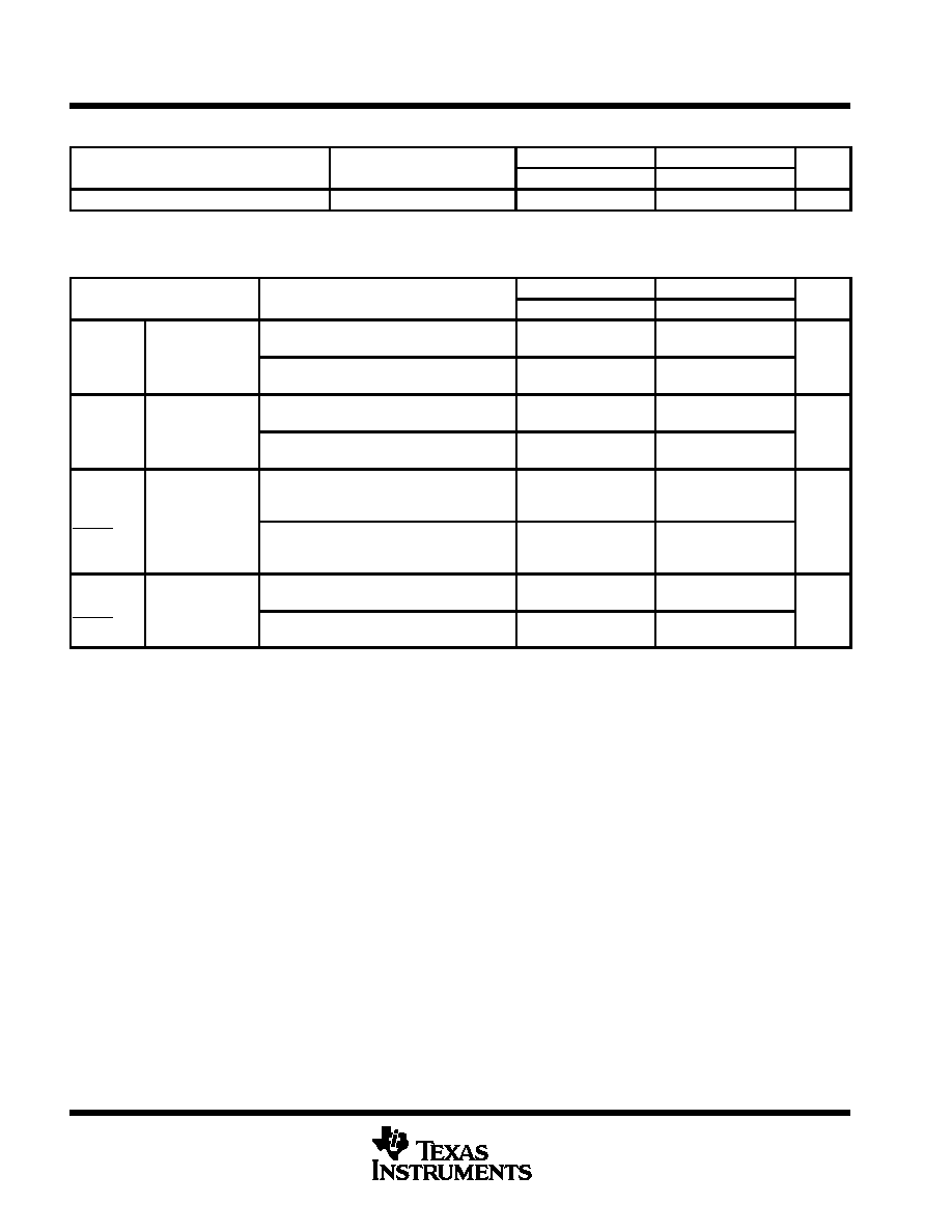
PARAMETER
TEST CONDITIONS
6N135
6N136, HCPL4502
UNIT
PARAMETER
TEST CONDITIONS
MIN
TYP
MAX
MIN
TYP
MAX
UNIT
VF
Input forward voltage
IF = 16 mA,
TA = 25
∞
C
1.6
1.7
1.6
1.7
V
VF
Temperature coefficient of
forward voltage
IF = 16 mA
≠ 1.8
≠ 1.8
mV/
∞
C
VBR
Input breakdown voltage
IR = 10
µ
A,
TA = 25
∞
C
5
5
V
VOL
Low level output voltage
VCC = 4.5 V,
IF 16 mA
IOL = 1.1 mA
0.1
0.4
V
VOL
Low-level output voltage
IF = 16 mA,
IB = 0
IOL = 2.4 mA
0.1
0.4
V
I
High level output current
IF = 0,
IB 0
VCC = VO = 5.5 V
3
500
3
500
nA
IOH
High-level output current
IB = 0,
TA = 25
∞
C
VCC = VO = 15 V
0.01
1
0.01
1
µ
A
IOH
High-level output current
VCC = 15 V,
IF = 0,
VO = 15 V,
IB = 0
50
50
µ
A
ICCH
Supply current, high-level
output
VCC = 15 V,
IF = 0,
TA = 25
∞
C
IO = 0,
IB = 0,
0.02
1
0.02
1
µ
A
ICCH
Supply current, high-level
output
VCC = 15 V,
IF = 0,
IO = 0,
IB = 0
2
2
µ
A
ICCL
Supply current, low-level
output
VCC = 15 V,
IF = 16 mA,
IO = 0,
IB = 0
40
40
µ
A
hFE
Transistor forward current
transfer ratio
VO = 5 V,
IO = 3 mA
100
100
(6N136
only)
CTR
Current transfer ratio
VCC = 4.5 V,
IF = 16 mA,
TA = 25
∞
C,
VO = 0.4 V,
IB = 0,
See Note 5
7%
18%
19%
24%
CTR
Current transfer ratio
VCC = 4.5 V,
IF = 16 mA,
See Note 5
VO = 0.5 V,
IB = 0,
5%
15%
rIO
Input-output resistance
VIO = 500 V,
See Note 6
TA = 25
∞
C,
1012
1012
IIO
Input-output insulation
leakage current
VIO = 3000 V,
TA = 25
∞
C,
See Note 6
t = 5 s,
RH = 45%,
1
1
µ
A
Ci
Input capacitance
VF = 0,
f = 1 MHz
60
60
pF
Cio
Input-output capacitance
f = 1 MHz,
See Note 6
0.6
0.6
pF
All typical values are at TA = 25
∞
C.
JEDEC registered data for 6N135 and 6N136
NOTES:
5. Current transfer ratio is defined as the ratio of output collector current IO to the forward LED input current IF times 100%.
6. These parameters are measured with terminals 2 and 3 shorted together and terminals 5, 6, 7, and 8 shorted together.
6N135, 6N136, HCPL4502
OPTOCOUPLERS/OPTOISOLATORS
SOES022A ≠ JULY 1986 ≠ REVISED APRIL 1998
4
POST OFFICE BOX 655303
∑
DALLAS, TEXAS 75265
operating characteristics, V
CC
= 5 V, I
F
= 16 mA, T
A
= 25
∞
C (unless otherwise noted)
PARAMETER
TEST CONDITIONS
6N135
6N136, HCPL4502
UNIT
PARAMETER
TEST CONDITIONS
MIN
TYP
MAX
MIN
TYP
MAX
UNIT
BW
Bandwidth (≠ 3 dB)
RL = 100
,
See Note 7
2
2
MHz
NOTE 7: Bandwidth is the range of frequencies within which the ac output voltage is not more than 3 dB below the low-frequency value.
switching characteristics at V
CC
= 5 V, I
F
= 16 mA, T
A
= 25
∞
C
PARAMETER
TEST CONDITIONS
6N135
6N136, HCPL4502
UNIT
PARAMETER
TEST CONDITIONS
MIN
TYP
MAX
MIN
TYP
MAX
UNIT
t
Propagation delay
time low to high
RL = 4.1 k
,
See Figure 1
See Note 8,
1
1.5
µ
s
tPLH
time, low-to-high-
level output
RL = 1.9 k
,
See Figure 1
See Note 9,
0.6
0.8
µ
s
t
Propagation delay
time high to low
RL = 4.1 k
,
See Figure 1
See Note 8,
0.7
1.5
µ
s
tPHL
time, high-to-low-
level output
RL = 1.9 k
,
See Figure 1
See Note 9,
0.6
0.8
µ
s
dV
CM
Common-mode
input transient
VCM = 10 V,
RL = 4.1 k
,
See Figure 2
IF = 0,
See Notes 8 and 10,
1000
V/
µ
s
CM
dt
(H)
immunity,
high-level output
VCM = 10 V,
RL = 1.9 k
,
See Figure 2
IF = 0,
See Notes 9 and 10,
1000
V/
µ
s
dV
CM
Common-mode
input transient
VCM = 10 V,
See Notes 9 and 10,
RL = 4.1 k
,
See Figure 2
1000
V/
µ
s
CM
dt
(L)
immunity,
low-level output
VCM = 10 V,
See Notes 9 and 10,
RL = 1.9 k
,
See Figure 2
1000
V/
µ
s
JEDEC registered data for 6N135 and 6N136
NOTES:
8. The 4.1-k
load represents one LSTTL unit load of 0.36 mA and a 6.1-k
pullup resistor.
9. The 1.9-k
load represents one TTL unit load of 1.6 mA and a 5.6-k
pullup resistor.
10. Common-mode transient immunity, high-level output, is the maximum rate of rise of the common-mode input voltage that does not
cause the output voltage to drop below 2 V. Common-mode input transient immunity, low-level output, is the maximum rate of fall
of the common-mode input voltage that does not cause the output voltage to rise above 0.8 V.
6N135, 6N136, HCPL4502
OPTOCOUPLERS/OPTOISOLATORS
SOES022A ≠ JULY 1986 ≠ REVISED APRIL 1998
5
POST OFFICE BOX 655303
∑
DALLAS, TEXAS 75265
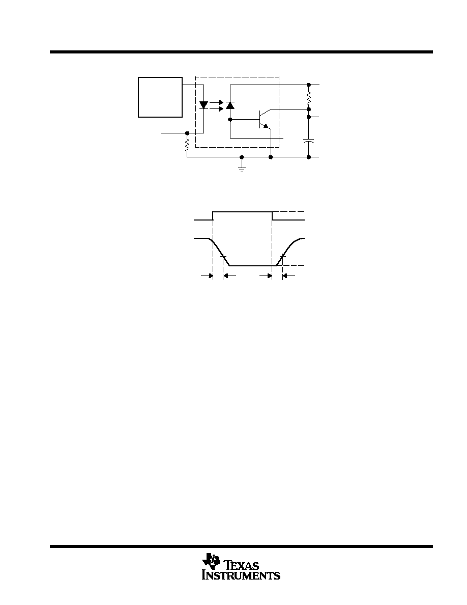
PARAMETER MEASUREMENT INFORMATION
GND
Open
Pulse
Generator
ZO = 50
tr = 5 ns
Input Current
Monitor
100
RL
Output
5 V
CL = 15 pF
(see Note A)
TEST CIRCUIT
1.5 V
1.5 V
tPHL
tPLH
IF
0 V
5 V
VOL
Input
Current
Output
Voltage
WAVEFORMS
NOTE A: CL includes probe and stray capacitance.
Figure 1. Switching Test Circuit and Waveforms

6N135, 6N136, HCPL4502
OPTOCOUPLERS/OPTOISOLATORS
SOES022A ≠ JULY 1986 ≠ REVISED APRIL 1998
6
POST OFFICE BOX 655303
∑
DALLAS, TEXAS 75265
PARAMETER MEASUREMENT INFORMATION
GND
Open
RL
Output
5 V
TEST CIRCUIT
VOLTAGE WAVEFORMS
IF
A
B
VFF
Generator
10 V
90%
90%
10%
10%
tr
tf
Generator
0 V
Output
Switch at A: IF = 0
Switch at B: IF = 16 mA
Output
5 V
VOL
dVCM
dt
8 V
tr or tf
=
tr = 8 ns TYP
tf = 8 ns TYP
Figure 2. Transient Immunity Test Circuit and Waveforms
6N135, 6N136, HCPL4502
OPTOCOUPLERS/OPTOISOLATORS
SOES022A ≠ JULY 1986 ≠ REVISED APRIL 1998
7
POST OFFICE BOX 655303
∑
DALLAS, TEXAS 75265
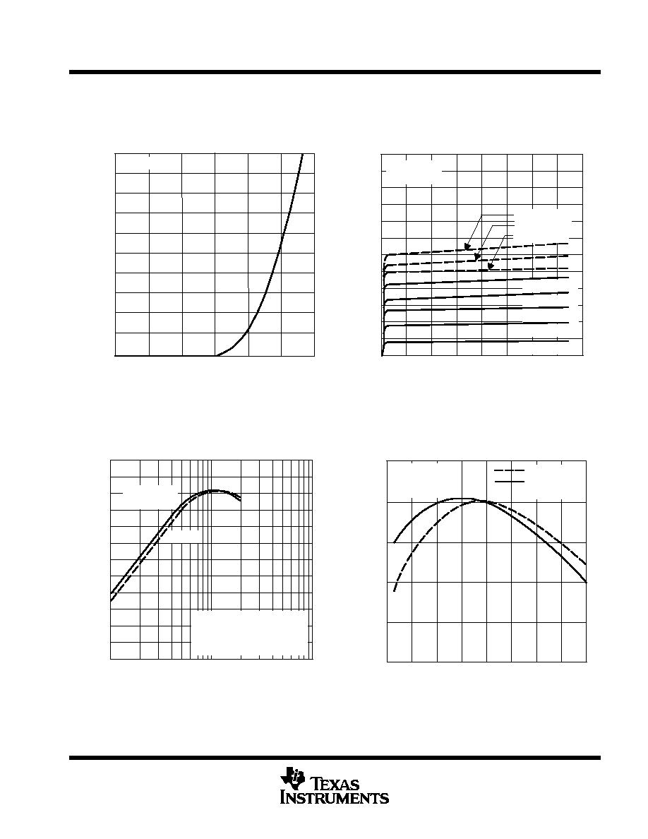
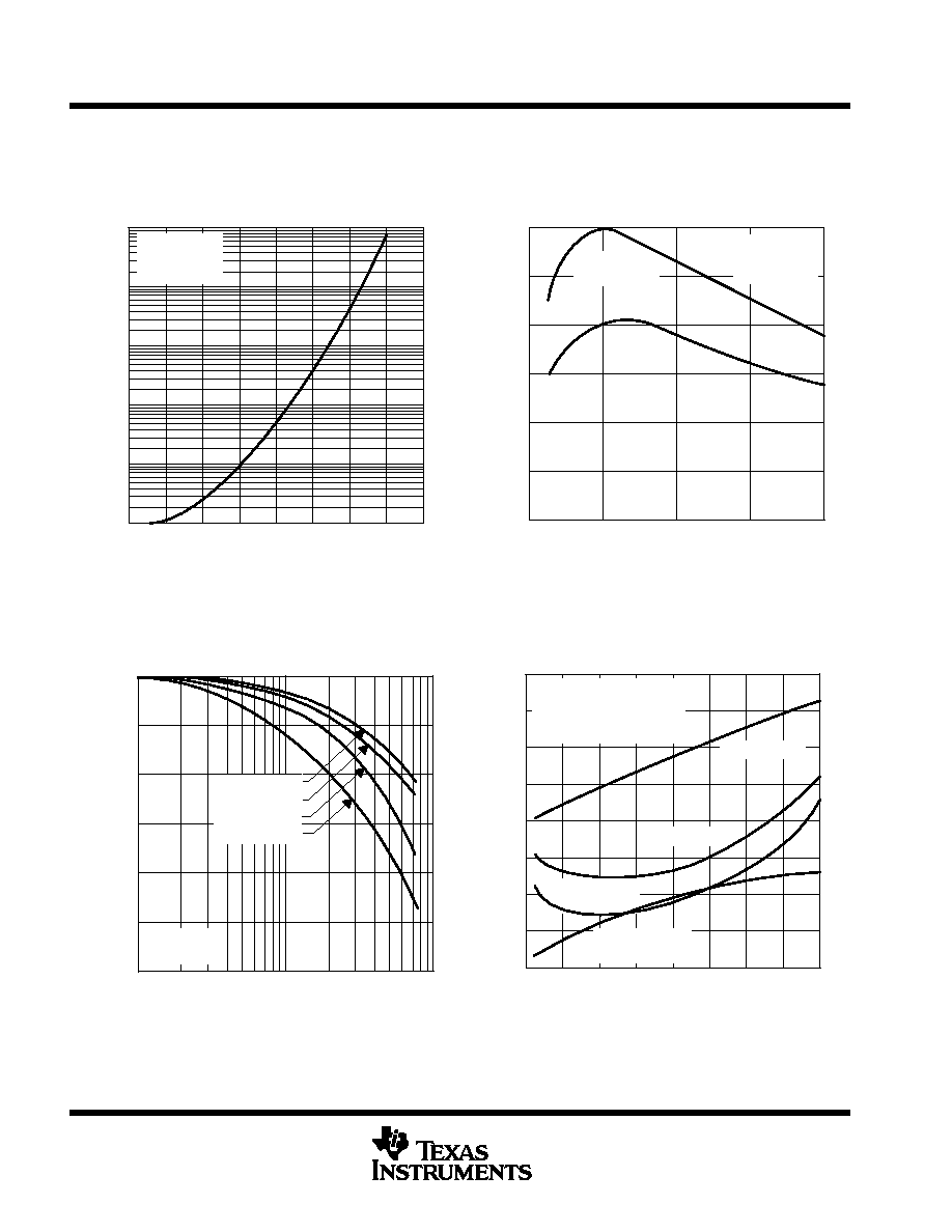
TYPICAL CHARACTERISTICS
Figure 3
10
8
4
2
0
18
6
1.1
1.2
1.3
1.4
14
12
16
INPUT-DIODE FORWARD CURRENT
vs
FORWARD VOLTAGE
20
1.5
1.6
1.7
VF ≠ Forward Voltage ≠ V
≠ Input-Diode Forward Current ≠ mA
I F
TA = 25
∞
C
Figure 4
7
5
3
0
0
4
6
10
≠ Output Current ≠ mA
9
6N135
CURRENT TRANSFER CHARACTERISTICS
12
14
16
2
8
12
11
10
8
6
4
2
1
I O
VO ≠ Output Voltage ≠ V
VCC = 5 V
TA = 25
∞
C
IF = 40 mA
IF = 35 mA
IF = 30 mA
IF = 25 mA
IF = 20mA
IF = 15mA
IF = 10mA
IF = 5 mA
Figure 5
0.6
0
1.2
1
2
4
7
10
40
100
CURRENT TRANSFER RATIO (NORMALIZED)
vs
INPUT DIODE FORWARD CURRENT
20
70
1.1
1
0.9
0.8
0.7
0.5
0.4
0.3
0.2
0.1
IF ≠ Input Diode Forward Current ≠ mA
6N136
HCPL4502
6N135
VCC = 5 V
VO = 0.4 V
TA = 25
∞
C
Normalized to IF = 16 mA
CTR ≠ Current T
ransfer
Ratio
(Normalized)
Figure 6
0.9
0.8
0.7
0.6
1
CURRENT TRANSFER RATIO (NORMALIZED)
vs
FREE-AIR TEMPERATURE
1.1
≠ 60
≠ 40
≠ 20
0
20
40
60
80
100
TA ≠ Free-Air Temperature ≠
∞
C
VCC = 5 V
VO = 0.4 V
IF = 16 mA
6N135
6N136,
HCPL4502
CTR ≠ Current T
ransfer
Ratio
(Normalized)
6N135, 6N136, HCPL4502
OPTOCOUPLERS/OPTOISOLATORS
SOES022A ≠ JULY 1986 ≠ REVISED APRIL 1998
8
POST OFFICE BOX 655303
∑
DALLAS, TEXAS 75265
TYPICAL CHARACTERISTICS
Figure 7
1
0.4
0.1
≠ High-Level Output Current ≠ nA
HIGH-LEVEL OUTPUT CURRENT
vs
FREE-AIR TEMPERATURE
10,000
10
4
100
40
1000
400
4000
≠ 75
≠ 50
≠2 5
0
25
50
75
100
125
I OH
TA ≠ Free-Air Temperature ≠
∞
C
VCC = 5 V
VO = 5 V
IF = 0
Figure 8
15
10
5
0
0
5
10
CTR(ac) ≠ Differential Current T
ransfer Ratio ≠ %
20
25
DIFFERENTIAL CURRENT TRANSFER RATIO
vs
INPUT-DIODE QUIESCENT FORWARD CURRENT
30
15
20
IF ≠ Input-Diode Quiescent Forward Current ≠ mA
VCC = 5 V
VO = 0.4 V
TA = 25
∞
C
6N136
HCPL4502
6N135
Figure 9
0.1
0.2
0.7 1
2
4
10
f ≠ Frequency ≠ MHz
FREQUENCY RESPONSE (NORMALIZED)
vs
FREQUENCY
0
≠ 5
≠ 10
≠ 15
≠ 20
≠ 25
≠ 30
0.4
7
RL = 100
RL = 220
RL = 470
RL = 1 k
IF = 16 mA
TA = 25
∞
C
Frequency Response (Normalized)
Figure 10
0.8
0.6
0.5
0.4
≠ Propagation Delay T
ime ≠
1
1.1
PROPAGATION DELAY TIME
vs
FREE-AIR TEMPERATURE
1.2
0.9
0.7
≠ 60
≠ 40
≠ 20
0
20
40
60
80
100
t
PLH
t
PHL
,
s
µ
TA ≠ Free-Air Temperature ≠
∞
C
VCC = 5 V
IF = 16 mA
RL = 4.1 k
for 6N135
RL = 1.9 k
for 6N136
6N135 tPLH
6N135 tPHL
6N136 tPHL
HCPL4502
6N136 tPLH
HCPL4502
6N135, 6N136, HCPL4502
OPTOCOUPLERS/OPTOISOLATORS
SOES022A ≠ JULY 1986 ≠ REVISED APRIL 1998
9
POST OFFICE BOX 655303
∑
DALLAS, TEXAS 75265
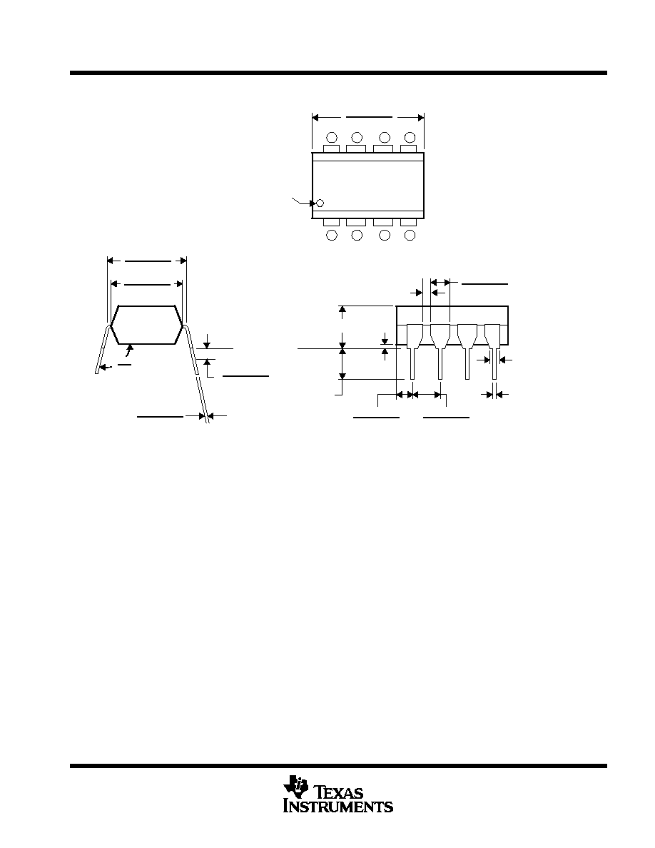
MECHANICAL INFORMATION
Gauge Plane
Seating Plane
C
L
L
C
8 Places
0,84 (0.033) MIN
2,79 (0.110)
2,29 (0.090)
3,17 (0.125) MIN
MIN
0,51 (0.020)
4,70 (0.185) MAX
1,78 (0,070)
1,14 (0.045)
Index Dot
9,91 (0.390)
9,49 (0.370)
0,76 (0.030)
0,00 (0.000)
105
∞
90
∞
8 Places
7,87 (0.310)
7,37 (0.290)
6,60 (0.260)
6,10 (0.240)
0,33 (0.013)
0,18 (0.007)
1,40 (0.055)
0,76 (0.030)
0, 457
±
0,076
(0.018
±
0.003)
8 Places
0,89 (0.035) MIN
1
2
3
4
8
7
6
5
NOTES: A. JEDEC registered data. This data sheet contains all applicable registered data in effect at the time of publication.
B. All linear dimensions are given in millimeters and parenthetically given in inches.
Figure 11. Packaging Specifications

PACKAGING INFORMATION
Orderable Device
Status
(1)
Package
Type
Package
Drawing
Pins Package
Qty
Eco Plan
(2)
Lead/Ball Finish
MSL Peak Temp
(3)
6N135
OBSOLETE
PDIP
N
8
TBD
Call TI
Call TI
6N136
OBSOLETE
PDIP
N
8
TBD
Call TI
Call TI
HCPL4502
OBSOLETE
PDIP
N
8
TBD
Call TI
Call TI
(1)
The marketing status values are defined as follows:
ACTIVE: Product device recommended for new designs.
LIFEBUY: TI has announced that the device will be discontinued, and a lifetime-buy period is in effect.
NRND: Not recommended for new designs. Device is in production to support existing customers, but TI does not recommend using this part in
a new design.
PREVIEW: Device has been announced but is not in production. Samples may or may not be available.
OBSOLETE: TI has discontinued the production of the device.
(2)
Eco
Plan
-
The
planned
eco-friendly
classification:
Pb-Free
(RoHS)
or
Green
(RoHS
&
no
Sb/Br)
-
please
check
http://www.ti.com/productcontent
for the latest availability information and additional product content details.
TBD: The Pb-Free/Green conversion plan has not been defined.
Pb-Free (RoHS): TI's terms "Lead-Free" or "Pb-Free" mean semiconductor products that are compatible with the current RoHS requirements
for all 6 substances, including the requirement that lead not exceed 0.1% by weight in homogeneous materials. Where designed to be soldered
at high temperatures, TI Pb-Free products are suitable for use in specified lead-free processes.
Green (RoHS & no Sb/Br): TI defines "Green" to mean Pb-Free (RoHS compatible), and free of Bromine (Br) and Antimony (Sb) based flame
retardants (Br or Sb do not exceed 0.1% by weight in homogeneous material)
(3)
MSL, Peak Temp. -- The Moisture Sensitivity Level rating according to the JEDEC industry standard classifications, and peak solder
temperature.
Important Information and Disclaimer:The information provided on this page represents TI's knowledge and belief as of the date that it is
provided. TI bases its knowledge and belief on information provided by third parties, and makes no representation or warranty as to the
accuracy of such information. Efforts are underway to better integrate information from third parties. TI has taken and continues to take
reasonable steps to provide representative and accurate information but may not have conducted destructive testing or chemical analysis on
incoming materials and chemicals. TI and TI suppliers consider certain information to be proprietary, and thus CAS numbers and other limited
information may not be available for release.
In no event shall TI's liability arising out of such information exceed the total purchase price of the TI part(s) at issue in this document sold by TI
to Customer on an annual basis.
PACKAGE OPTION ADDENDUM
www.ti.com
8-Apr-2005
Addendum-Page 1

IMPORTANT NOTICE
Texas Instruments Incorporated and its subsidiaries (TI) reserve the right to make corrections, modifications,
enhancements, improvements, and other changes to its products and services at any time and to discontinue
any product or service without notice. Customers should obtain the latest relevant information before placing
orders and should verify that such information is current and complete. All products are sold subject to TI's terms
and conditions of sale supplied at the time of order acknowledgment.
TI warrants performance of its hardware products to the specifications applicable at the time of sale in
accordance with TI's standard warranty. Testing and other quality control techniques are used to the extent TI
deems necessary to support this warranty. Except where mandated by government requirements, testing of all
parameters of each product is not necessarily performed.
TI assumes no liability for applications assistance or customer product design. Customers are responsible for
their products and applications using TI components. To minimize the risks associated with customer products
and applications, customers should provide adequate design and operating safeguards.
TI does not warrant or represent that any license, either express or implied, is granted under any TI patent right,
copyright, mask work right, or other TI intellectual property right relating to any combination, machine, or process
in which TI products or services are used. Information published by TI regarding third-party products or services
does not constitute a license from TI to use such products or services or a warranty or endorsement thereof.
Use of such information may require a license from a third party under the patents or other intellectual property
of the third party, or a license from TI under the patents or other intellectual property of TI.
Reproduction of information in TI data books or data sheets is permissible only if reproduction is without
alteration and is accompanied by all associated warranties, conditions, limitations, and notices. Reproduction
of this information with alteration is an unfair and deceptive business practice. TI is not responsible or liable for
such altered documentation.
Resale of TI products or services with statements different from or beyond the parameters stated by TI for that
product or service voids all express and any implied warranties for the associated TI product or service and
is an unfair and deceptive business practice. TI is not responsible or liable for any such statements.
Following are URLs where you can obtain information on other Texas Instruments products and application
solutions:
Products
Applications
Amplifiers
amplifier.ti.com
Audio
www.ti.com/audio
Data Converters
dataconverter.ti.com
Automotive
www.ti.com/automotive
DSP
dsp.ti.com
Broadband
www.ti.com/broadband
Interface
interface.ti.com
Digital Control
www.ti.com/digitalcontrol
Logic
logic.ti.com
Military
www.ti.com/military
Power Mgmt
power.ti.com
Optical Networking
www.ti.com/opticalnetwork
Microcontrollers
microcontroller.ti.com
Security
www.ti.com/security
Telephony
www.ti.com/telephony
Video & Imaging
www.ti.com/video
Wireless
www.ti.com/wireless
Mailing Address:
Texas Instruments
Post Office Box 655303 Dallas, Texas 75265
Copyright
2005, Texas Instruments Incorporated