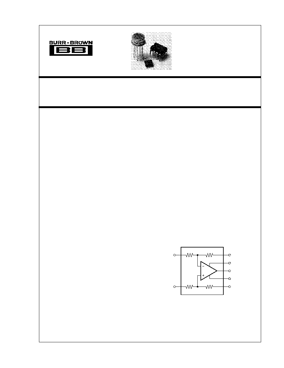
Precision Unity Gain Differential Amplifier
©
1985 Burr-Brown Corporation
PDS-617G
Printed in U.S.A. August, 1993
Precision Unity Gain
DIFFERENTIAL AMPLIFIER
INA105
DESCRIPTION
The INA105 is a monolithic Gain = 1 differential
amplifier consisting of a precision op amp and on-chip
metal film resistors. The resistors are laser trimmed
for accurate gain and high common-mode rejection.
Excellent TCR tracking of the resistors maintains
gain accuracy and common-mode rejection over
temperature.
The differential amplifier is the foundation of many
commonly used circuits. The INA105 provides this
precision circuit function without using an expensive
precision resistor network. The INA105 is available in
8-pin plastic DIP, SO-8 surface-mount and TO-99
metal packages.
Sense
V+
Output
V
Ref
In
+In
5
7
6
4
1
2
3
25k
25k
25k
25k
®
FEATURES
q
CMR 86dB min OVER TEMPERATURE
q
GAIN ERROR: 0.01% max
q
NONLINEARITY: 0.001% max
q
NO EXTERNAL ADJUSTMENTS
REQUIRED
q
EASY TO USE
q
COMPLETE SOLUTION
q
HIGHLY VERSATILE
q
LOW COST
q
PLASTIC DIP, TO-99 HERMETIC METAL,
AND SO-8 SOIC PACKAGES
APPLICATIONS
q
DIFFERENTIAL AMPLIFIER
q
INSTRUMENTATION AMPLIFIER
BUILDING BLOCK
q
UNITY-GAIN INVERTING AMPLIFIER
q
GAIN-OF-1/2 AMPLIFIER
q
NONINVERTING GAIN-OF-2 AMPLIFIER
q
AVERAGE VALUE AMPLIFIER
q
ABSOLUTE VALUE AMPLIFIER
q
SUMMING AMPLIFIER
q
SYNCHRONOUS DEMODULATOR
q
CURRENT RECEIVER WITH COMPLIANCE
TO RAILS
q
4mA TO 20mA TRANSMITTER
q
VOLTAGE-CONTROLLED CURRENT
SOURCE
q
ALL-PASS FILTERS
International Airport Industrial Park · Mailing Address: PO Box 11400, Tucson, AZ 85734 · Street Address: 6730 S. Tucson Blvd., Tucson, AZ 85706 · Tel: (520) 746-1111 · Twx: 910-952-1111
Internet: http://www.burr-brown.com/ · FAXLine: (800) 548-6133 (US/Canada Only) · Cable: BBRCORP · Telex: 066-6491 · FAX: (520) 889-1510 · Immediate Product Info: (800) 548-6132
SBOS145
®
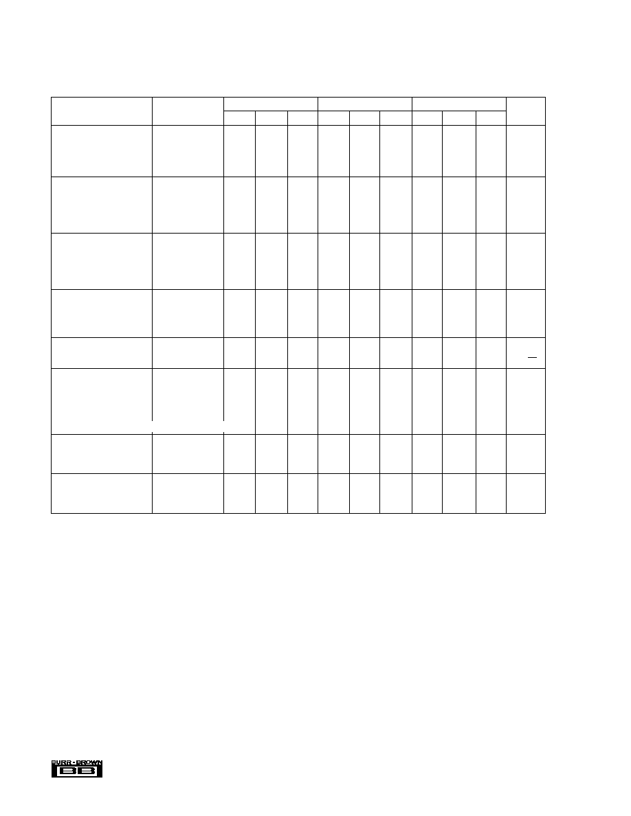
INA105
2
INA105AM
INA105BM
INA105KP, KU
PARAMETER
CONDITIONS
MIN
TYP
MAX
MIN
TYP
MAX
MIN
TYP
MAX
UNITS
SPECIFICATIONS
ELECTRICAL
At +25
°
C, V
CC
=
±
15V, unless otherwise noted.
The information provided herein is believed to be reliable; however, BURR-BROWN assumes no responsibility for inaccuracies or omissions. BURR-BROWN assumes
no responsibility for the use of this information, and all use of such information shall be entirely at the user's own risk. Prices and specifications are subject to change
without notice. No patent rights or licenses to any of the circuits described herein are implied or granted to any third party. BURR-BROWN does not authorize or warrant
any BURR-BROWN product for use in life support devices and/or systems.
GAIN
Initial
(1)
1
T
T
V/V
Error
0.005
0.01
T
T
0.01
0.025
%
vs Temperature
1
5
T
T
T
T
ppm/
°
C
Nonlinearity
(2)
0.0002
0.001
T
T
T
T
%
OUTPUT
Rated Voltage
I
O
= +20mA, 5mA
10
12
T
T
T
T
V
Rated Current
V
O
= 10V
+20, 5
T
T
mA
Impedance
0.01
T
T
Current Limit
To Common
+40/10
T
T
mA
Capacitive Load
Stable Operation
1000
T
T
pF
INPUT
Impedance
(3)
Differential
50
T
T
k
Common-Mode
50
T
T
k
Voltage Range
(4)
Differential
±
10
T
T
V
Common-Mode
±
20
T
T
V
Common-Mode Rejection
(5)
T
A
= T
MIN
to T
MAX
80
90
86
100
72
T
dB
OFFSET VOLTAGE
RTO
(6), (7)
Initial
50
250
T
T
T
500
µ
V
vs Temperature
5
20
5
10
T
T
µ
V/
°
C
vs Supply
±
V
S
= 6V to 18V
1
25
T
15
T
T
µ
V/V
vs Time
20
T
T
µ
V/mo
OUTPUT NOISE VOLTAGE
RTO
(6), (8)
f
B
= 0.01Hz to 10Hz
2.4
T
T
µ
Vp-p
f
O
= 10kHz
60
T
T
nV/
Hz
DYNAMIC RESPONSE
Small Signal Bandwidth
3dB
1
T
T
MHz
Full Power Bandwidth
V
O
= 20Vp-p
30
50
T
T
T
T
kHz
Slew Rate
2
3
T
T
T
T
V/
µ
s
Settling Time: 0.1%
V
O
= 10V Step
4
T
T
µ
s
0.01%
V
O
= 10V Step
5
T
T
µ
s
0.01%
V
CM
= 10V Step, V
DIFF
= 0V
1.5
T
T
µ
s
POWER SUPPLY
Rated
±
15
T
T
V
Voltage Range
Derated Performance
±
5
±
18
T
T
T
T
V
Quiescent Current
V
O
= 0V
±
1.5
±
2
T
T
T
T
mA
TEMPERATURE RANGE
Specification
40
+85
T
T
T
T
°
C
Operation
55
+125
T
T
40
+85
°
C
Storage
65
+150
T
T
40
+125
°
C
T
Specification same as for INA105AM.
NOTES: (1) Connected as difference amplifier (see Figure 4). (2) Nonlinearity is the maximum peak deviation from the best-fit straight line as a percent of full-scale peak-
to-peak output. (3) 25k
resistors are ratio matched but have
±
20% absolute value. (4) Maximum input voltage without protection is 10V more than either
±
15V supply
(
±
25V). Limit I
IN
to 1mA. (5) With zero source impedance (see "Maintaining CMR" section). (6) Referred to output in unity-gain difference configuration. Note that this
circuit has a gain of 2 for the operational amplifier's offset voltage and noise voltage. (7) Includes effects of amplifier's input bias and offset currents. (8) Includes effects
of amplifier's input current noise and thermal noise contribution of resistor network.
®
INA105
3
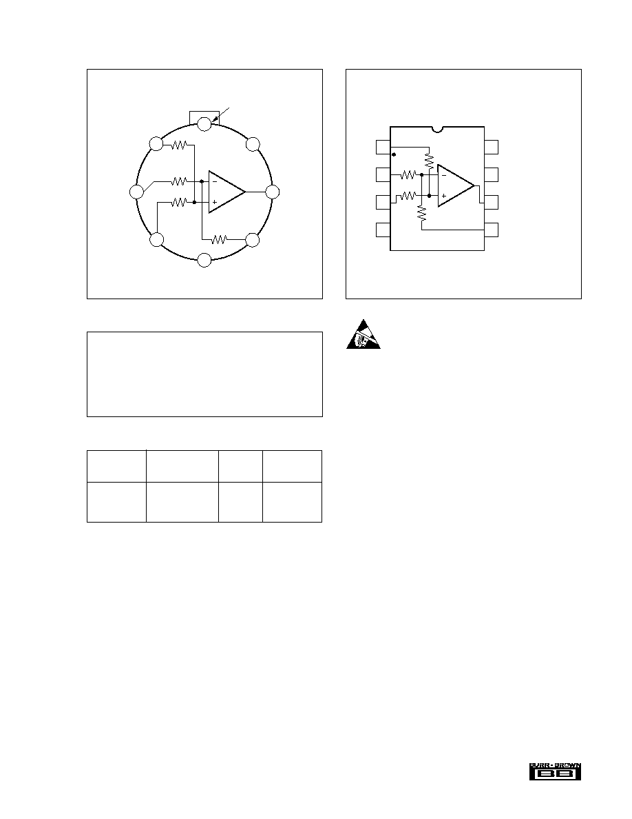
PIN CONFIGURATIONS
Top View
TO-99
INA105AM
INA105BM
NOTE: (1) Performance grade identifier box for small outline surface mount.
Blank indicates K grade. Part is marked INA105U.
Ref
In
+In
V
No Internal Connection
V+
Output
Sense
1
2
3
4
8
7
6
5
(1)
8
7
6
2
1
3
4
5
Tab
No Internal
Connection
Output
V+
V
Sense
Ref
In
+In
Case internally connected to V. Make no connection.
Top View
DIP/SOIC
ELECTROSTATIC
DISCHARGE SENSITIVITY
This integrated circuit can be damaged by ESD. Burr-Brown
recommends that all integrated circuits be handled with
appropriate precautions. Failure to observe proper handling
and installation procedures can cause damage.
ESD damage can range from subtle performance degradation
to complete device failure. Precision integrated circuits may
be more susceptible to damage because very small parametric
changes could cause the device not to meet its published
specifications.
ABSOLUTE MAXIMUM RATINGS
Supply ................................................................................................
±
18V
Input Voltage Range ............................................................................
±
V
S
Operating Temperature Range: M .................................. 55
°
C to +125
°
C
P, U ................................ 40
°
C to +85
°
C
Storage Temperature Range: M ..................................... 65
°
C to +150
°
C
P, U ................................. 40
°
C to +125
°
C
Lead Temperature (soldering, 10s) M, P ....................................... +300
°
C
Wave Soldering (3s, max) U .......................................................... +260
°
C
Output Short Circuit to Common .............................................. Continuous
PACKAGE
DRAWING
TEMPERATURE
PRODUCT
PACKAGE
NUMBER
(1)
RANGE
INA105AM
TO-99 Metal
001
40
°
C to +85
°
C
INA105BM
TO-99 Metal
001
40
°
C to +85
°
C
INA105KP
8-Pin Plastic DIP
006
40
°
C to +85
°
C
INA105KU
8-Pin SOIC
182
40
°
C to +85
°
C
NOTE: (1) For detailed drawing and dimension table, please see end of data
sheet, or Appendix C of Burr-Brown IC Data Book.
PACKAGE/ORDERING INFORMATION
®
INA105
4
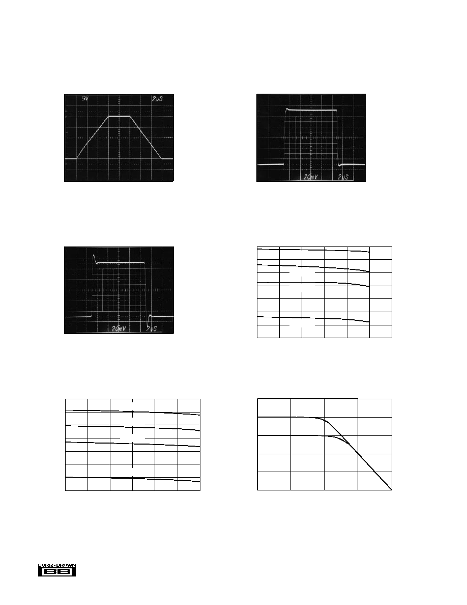
SMALL SIGNAL RESPONSE
(No Load)
Time (µs)
Output Voltage (mV)
0
5
10
+50
0
50
STEP RESPONSE
Time (µs)
Output Voltage (V)
10 to +10
0
4
8
12
16
SMALL SIGNAL RESPONSE
(R
LOAD
= , C
LOAD
= 1000pF)
Time (µs)
Output Voltage (mV)
0
5
10
+50
0
50
MAXIMUM V
OUT
vs I
OUT
(Negative Swing)
I
OUT
(mA)
0
V
OUT
(V)
17.5
15
12.5
10
7.5
5
2.5
0
2
4
6
8
10
12
V
S
= ±5V
V
S
= ±12V
V
S
= ±15V
V
S
= ±18V
CMR vs FREQUENCY
Frequency (Hz)
10
CMR (dB)
110
100
90
80
70
60
100
1k
10k
100k
AM, KP, U
BM
MAXIMUM V
OUT
vs I
OUT
(Positive Swing)
I
OUT
(mA)
0
V
OUT
(V)
17.5
15
12.5
10
7.5
5
2.5
0
6
12
18
24
30
36
V
S
= ±5V
V
S
= ±12V
V
S
= ±15V
V
S
= ±18V
TYPICAL PERFORMANCE CURVES
At T
A
= 25
°
C, V
S
=
±
15V, unless otherwise noted.
®
INA105
5
COMMON-MODE INPUT RANGE vs SUPPLY
(Difference Amplifier Connected, V
OUT
= 0)
Supply Voltage (V)
±3
Input Range (V)
36
30
24
18
12
6
0
±6
±9
±12
±15
±18
±21
Negative CMV
Positive CMV
POWER SUPPLY REJECTION
vs FREQUENCY
Frequency (Hz)
1
PSRR (dB)
140
120
100
80
60
40
10
100
1k
10k
100k
V
V+
TYPICAL PERFORMANCE CURVES
(CONT)
At T
A
= 25
°
C, V
S
=
±
15V, unless otherwise noted.
APPLICATION INFORMATION
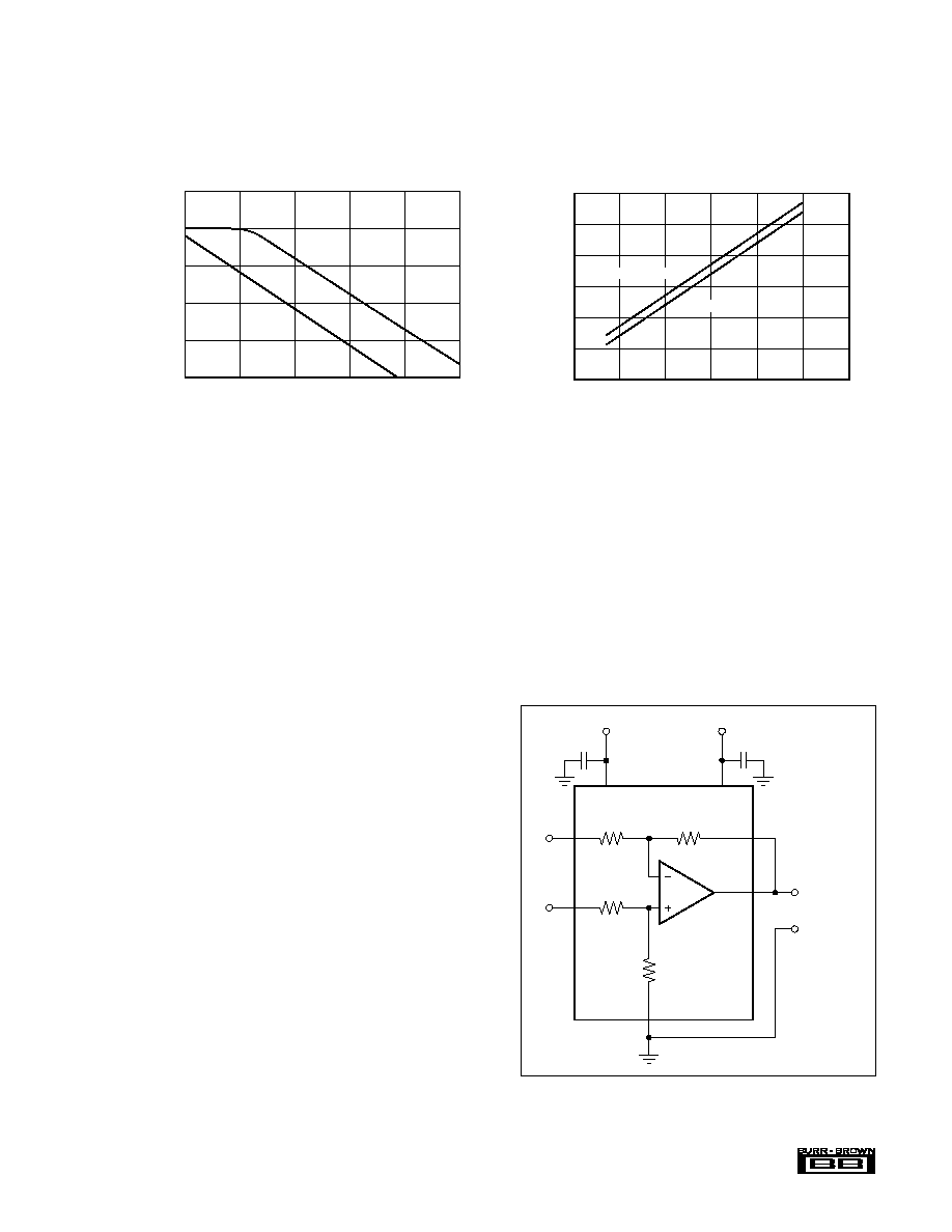
Figure 1 shows the basic connections required for operation
of the INA105. Power supply bypass capacitors should be
connected close to the device pins.
The differential input signal is connected to pins 2 and 3 as
shown. The source impedances connected to the inputs must
be nearly equal to assure good common-mode rejection. A
5
mismatch in source impedance will degrade the com-
mon-mode rejection of a typical device to approximately
80dB. If the source has a known mismatch in source imped-
ance, an additional resistor in series with one input can be
used to preserve good common-mode rejection.
The output is referred to the output reference terminal (pin
1) which is normally grounded. A voltage applied to the Ref
terminal will be summed with the output signal. This can be
used to null offset voltage as shown in Figure 2. The source
impedance of a signal applied to the Ref terminal should be
less than 10
to maintain good common-mode rejection.
Do not interchange pins 1 and 3 or pins 2 and 5, even though
nominal resistor values are equal. These resistors are laser
trimmed for precise resistor ratios to achieve accurate gain
and highest CMR. Interchanging these pins would not pro-
vide specified performance.
FIGURE 1. Basic Power Supply and Signal Connections.
V
3
5
6
3
INA105
V
OUT
= V
3
V
2
2
R
3
R
1
R
2
R
4
V
2
25k
25k
25k
25k
1µF
V
4
1µF
V+
7
1