INA138
INA168
FEATURES
q
COMPLETE UNIPOLAR HIGH-SIDE
CURRENT MEASUREMENT CIRCUIT
q
WIDE SUPPLY AND COMMON-MODE RANGE
q
INA138: 2.7V to 36V
q
INA168: 2.7V to 60V
q
INDEPENDENT SUPPLY AND INPUT COMMON-
MODE VOLTAGES
q
SINGLE RESISTOR GAIN SET
q
LOW QUIESCENT CURRENT (25
µ
A typ)
q
WIDE TEMPERATURE RANGE: ≠40
∞
C to +125
∞
C
q
SOT23-5 PACKAGE
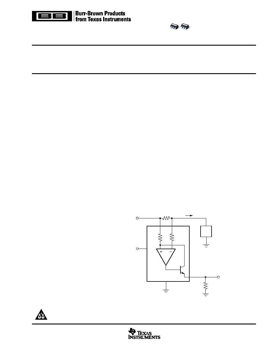
High-Side Measurement
CURRENT SHUNT MONITOR
DESCRIPTION
The INA138 and INA168 are high-side, unipolar, current
shunt monitors. Wide input common-mode voltage range,
low quiescent current, and tiny SOT23 packaging enable use
in a variety of applications.
Input common-mode and power-supply voltages are inde-
pendent and can range from 2.7V to 36V for the INA138 and
2.7V to 60V for the INA168. Quiescent current is only 25
µ
A,
which permits connecting the power supply to either side of
the current measurement shunt with minimal error.
The device converts a differential input voltage to a current
output. This current is converted back to a voltage with an
external load resistor that sets any gain from 1 to over 100.
Although designed for current shunt measurement, the circuit
invites creative applications in measurement and level shifting.
Both the INA138 and INA168 are available in SOT23-5 and
are specified for the ≠40
∞
C to +125
∞
C temperature range.
APPLICATIONS
q
CURRENT SHUNT MEASUREMENT:
Automotive, Telephone, Computers
q
PORTABLE AND BATTERY-BACKUP
SYSTEMS
q
BATTERY CHARGERS
q
POWER MANAGEMENT
q
CELL PHONES
q
PRECISION CURRENT SOURCE
R
S
2
1
OUT
GND
R
L
V
O
= I
S
R
S
R
L
/5k
Load
5k
5k
V
IN+
Up To 60V
V
IN+
V
IN≠
3
4
I
S
V+
5
www.ti.com
PRODUCTION DATA information is current as of publication date.
Products conform to specifications per the terms of Texas Instruments
standard warranty. Production processing does not necessarily include
testing of all parameters.
Copyright © 1999, 2002 Texas Instruments Incorporated
Please be aware that an important notice concerning availability, standard warranty, and use in critical applications of
Texas Instruments semiconductor products and disclaimers thereto appears at the end of this data sheet.
SBOS122A ≠ DECEMBER 1999 ≠ REVISED DECEMBER 2002
INA138, INA168
2
SBOS122A
www.ti.com
Supply Voltage, V+
INA138 ............................................................................... ≠0.3V to 60V
INA168 ............................................................................... ≠0.3V to 75V
Analog Inputs, V
IN+
, V
IN≠
INA138
Common Mode ............................................................... ≠0.3V to 60V
Differential (V
IN+
) ≠ (V
IN≠
) .................................................. ≠40V to 2V
INA168
Common Mode ............................................................... ≠0.3V to 75V
Differential (V
IN+
) ≠ (V
IN≠
) .................................................. ≠40V to 2V
Analog Output, Out .............................................................. ≠0.3V to 40V
Operating Temperature .................................................. ≠55
∞
C to +150
∞
C
Storage Temperature ..................................................... ≠55
∞
C to +150
∞
C
Junction Temperature .................................................................... +150
∞
C
Lead Temperature (soldering, 10s) ............................................... +300
∞
C
NOTE: (1) Stresses above these ratings may cause permanent damage.
Exposure to absolute maximum conditions for extended periods may degrade
device reliability. These are stress ratings only, and functional operation of the
device at these or any other conditions beyond those specified is not implied.
ABSOLUTE MAXIMUM RATINGS
(1)
SPECIFIED
PACKAGE
TEMPERATURE
PACKAGE
ORDERING
TRANSPORT
PRODUCT
PACKAGE-LEAD
DESIGNATOR
(1)
RANGE
MARKING
NUMBER
MEDIA, QUANTITY
INA138
SOT23-5 Surface-Mount
DBV
≠40
∞
C to +125
∞
C
B38
INA138NA/250
Tape and Reel, 250
"
"
"
"
"
INA138NA/3K
Tape and Reel, 3000
INA168
SOT23-5 Surface-Mount
DBV
≠40
∞
C to +125
∞
C
A68
INA168NA/250
Tape and Reel, 250
"
"
"
"
"
INA168NA/3K
Tape and Reel, 3000
NOTE: (1) For the most current specifications and package information, refer to our web site at www.ti.com.
PACKAGE/ORDERING INFORMATION
PIN CONFIGURATION
Top View
SOT23
OUT
GND
V
IN+
V+
V
IN≠
1
2
3
5
4
ELECTROSTATIC
DISCHARGE SENSITIVITY
This integrated circuit can be damaged by ESD. Texas Instru-
ments recommends that all integrated circuits be handled with
appropriate precautions. Failure to observe proper handling
and installation procedures can cause damage.
ESD damage can range from subtle performance degrada-
tion to complete device failure. Precision integrated circuits
may be more susceptible to damage because very small
parametric changes could cause the device not to meet its
published specifications.
INA138, INA168
3
SBOS122A
www.ti.com
ELECTRICAL CHARACTERISTICS
Boldface limits apply over the specified temperature range, T
A
= ≠40
∞
C to +125
∞
C.
All other characteristics at T
A
= +25
∞
C, V
S
= 5V, V
IN+
= 12V, and R
OUT
= 125k
, unless otherwise noted.
PARAMETER
CONDITION
MIN
TYP
MAX
MIN
TYP
MAX
UNITS
INPUT
Full-Scale Sense Voltage
V
SENSE
= V
IN+
≠ V
IN≠
100
500
mV
Common-Mode Input Range
2.7
36
60
V
Common-Mode Rejection
V
IN+
= 2.7V to 40V, V
SENSE
= 50mV
100
120
dB
V
IN+
= 2.7V to 60V, V
SENSE
= 50mV
100
120
dB
Offset Voltage
(1)
±
0.2
±
1
mV
Over Temperature
±
2
mV
vs Temperature
1
µ
V/
∞
C
vs Power Supply, V+
V≠
= 2.7V to 40V, V
SENSE
= 50mV
0.1
10
µ
V/V
V≠
= 2.7V to 60V, V
SENSE
= 50mV
0.1
10
µ
V/V
Input Bias Current
V
IN+
≠ V
IN≠
2
µ
A
vs Temperature
10
µ
A
OUTPUT
Transconductance
T
A
= +25
∞
C, V
SENSE
= 10mV
≠ 150mV
198
200
202
µ
A/V
Over Temperature
196
204
µ
A/V
vs Temperature
V
SENSE
= 100mV
10
nA/
∞
C
Nonlinearity Error
V
SENSE
= 10mV
to 150mV
±
0.01
±
0.1
%
Total Output Error
V
SENSE
= 100mV
±
0.5
±
2
%
Over Temperature
±
2.5
%
Output Impedance
1 || 5
G
|| pF
Voltage Output
Swing to Power Supply, V+
(V+) ≠ 0.8 (V+) ≠ 1.0
V
Swing to Common Mode, V
CM
V
CM
≠ 0.5 V
CM
≠ 0.8
V
FREQUENCY RESPONSE
Bandwidth
R
OUT
= 5k
800
kHz
R
OUT
= 125k
32
kHz
Settling Time (0.1%)
5V Step, R
OUT
= 5k
1.8
µ
s
5V Step, R
OUT
= 125k
30
µ
s
NOISE
Output-Current Noise Density
9
pA/
Hz
Total Output-Current Noise
BW = 100kHz
3
nA RMS
POWER SUPPLY
Operating Range, V+
2.7
36
60
V
Quiescent Current
T
A
= +25
∞
C, V
SENSE
= 0, I
O
= 0
25
45
µ
A
Over Temperature
60
µ
A
TEMPERATURE RANGE
Specification, T
MIN
to T
MAX
≠40
125
∞
C
Operating
≠55
150
∞
C
Storage
≠65
150
∞
C
Thermal Resistance
JA
200
∞
C/W
specification same as INA138NA
NOTE: (1) Defined as the amount of input voltage, V
SENSE
, to drive the output to zero.
INA138NA
INA168NA
INA138, INA168
4
SBOS122A
www.ti.com
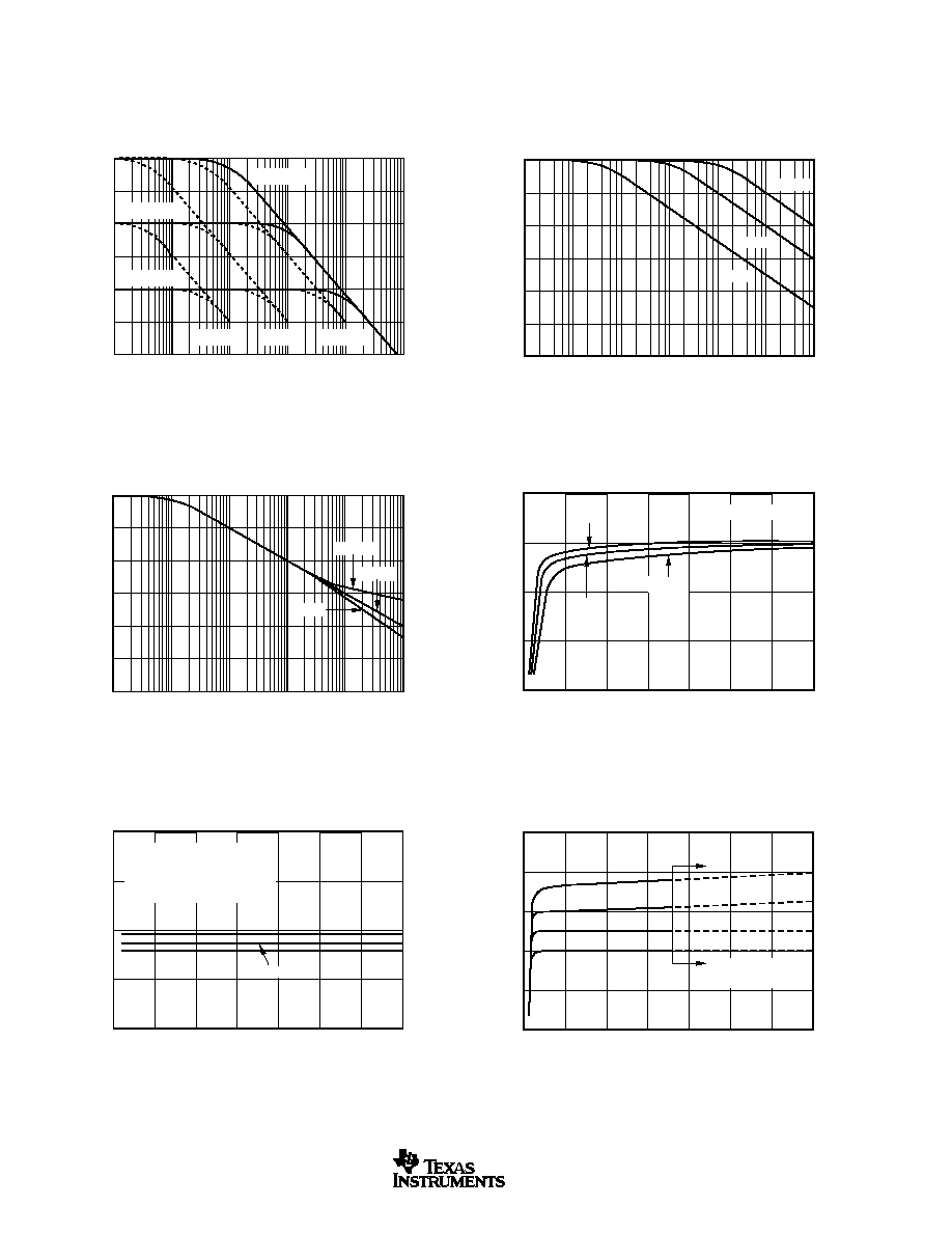
TYPICAL CHARACTERISTICS
At T
A
= +25
∞
C, V+ = 5V, V
IN+
= 12V, and R
L
= 125k
, unless otherwise noted.
40
30
20
10
0
≠10
≠20
100
1k
10k
100k
1M
10M
Gain (dB)
Frequency (Hz)
GAIN vs FREQUENCY
R
L
= 50k
R
L
= 500k
C
L
= 10nF
C
L
= 1nF
C
L
= 100pF
R
L
= 5k
120
100
80
60
40
20
0
0.1
1
10
100
1k
10k
Common-Mode Rejection (dB)
Frequency (Hz)
100k
G = 1
G = 10
G = 100
COMMON-MODE REJECTION vs FREQUENCY
140
120
100
80
60
40
20
1
10
100
1k
10k
100k
Power-Supply Rejection (dB)
Frequency (Hz)
POWER-SUPPLY REJECTION vs FREQUENCY
G = 1
G = 10
G = 100
5
0
≠5
≠10
≠15
0
25
50
75
100
125
Total Output Error (%)
V
IN
(mV)
TOTAL OUTPUT ERROR vs V
IN
150
200
≠55
∞
C
+25
∞
C
+150
∞
C
V
IN
= (V
IN+
≠ V
IN≠
)
2
1
0
≠1
≠2
0
10
20
30
40
50
Total Output Error (%)
Power-Supply Voltage (V)
TOTAL OUTPUT ERROR
vs POWER-SUPPLY VOLTAGE
60
70
G = 1
G = 10
G = 25
Output error is essentially
independent of both
V+ supply voltage and
input common-mode voltage.
50
40
30
20
10
0
0
10
20
30
40
50
Quiescent Current (
µ
A)
Power-Supply Voltage (V)
QUIESCENT CURRENT
vs POWER-SUPPLY VOLTAGE
60
70
+150
∞
+125
∞
+25
∞
≠55
∞
Use INA168 with
(V+) > 36V
INA138, INA168
5
SBOS122A
www.ti.com
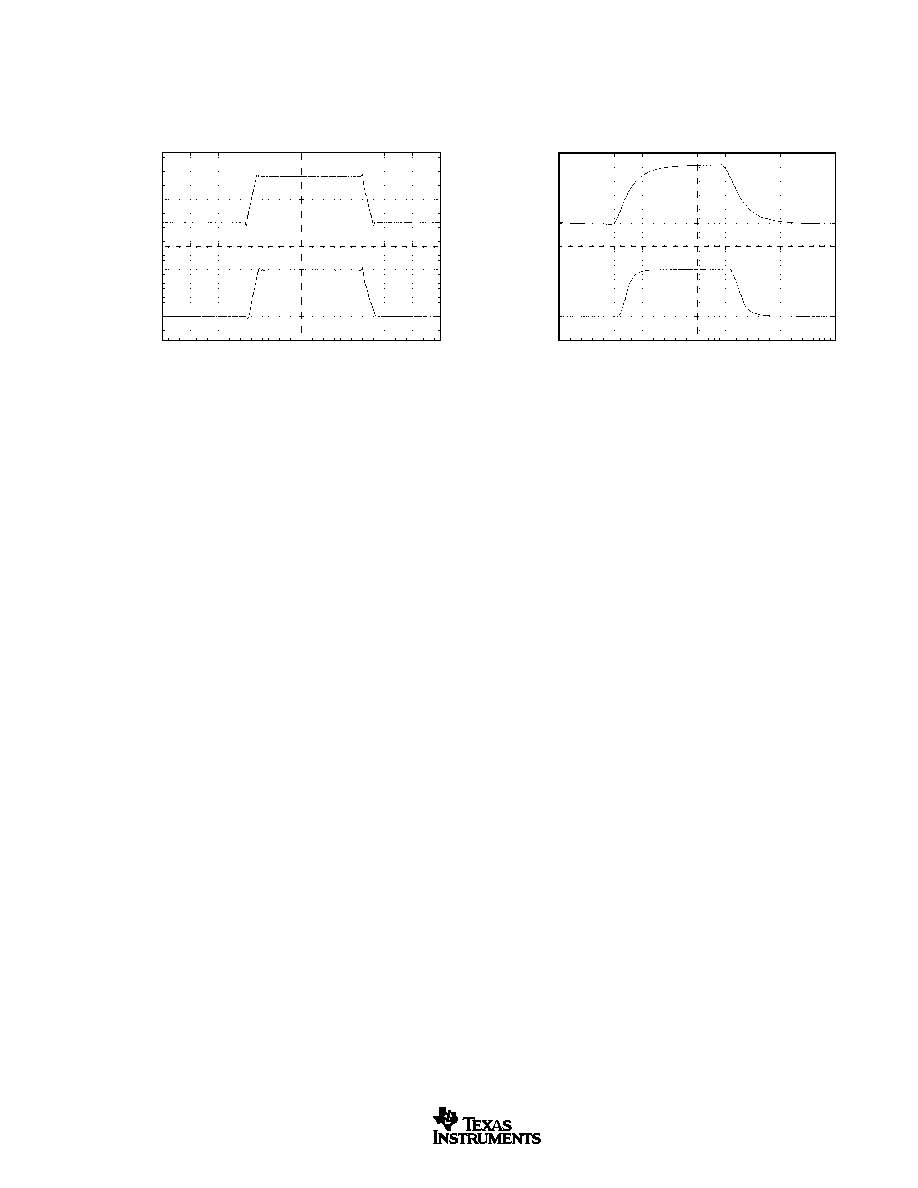
TYPICAL CHARACTERISTICS
(Cont.)
At T
A
= +25
∞
C, V+ = 5V, V
IN+
= 12V, and R
L
= 125k
, unless otherwise noted.
STEP RESPONSE
10
µ
s/div
200mV
G = 1
100mV
100mV
G = 1
0mV
50mV/div
STEP RESPONSE
10
µ
s/div
G = 25
0V
G = 10
0V
1V/div
500mV/div
OPERATION
Figure 1 illustrates the basic circuit diagram for both the
INA138 and INA168. Load current I
S
is drawn from supply V
S
through shunt resistor R
S
. The voltage drop in shunt resistor
V
S
is forced across R
G1
by the internal op amp, causing
current to flow into the collector of Q1. External resistor R
L
converts the output current to a voltage, V
OUT
, at the OUT pin.
The transfer function for the INA138 is:
I
O
= g
m
(V
IN+
≠ V
IN≠
)
(1)
where g
m
= 200
µ
A/V.
In the circuit of Figure 1, the input voltage, (V
IN+
≠ V
IN≠
), is
equal to I
S
∑ R
S
and the output voltage, V
OUT
, is equal to
I
O
∑ R
L
. The transconductance, g
m
, of the INA138 is
200
µ
A/V. The complete transfer function for the current
measurement amplifier in this application is:
V
OUT
= (I
S
) (R
S
) (200
µ
A/V) (R
L
)
(2)
The maximum differential input voltage for accurate mea-
surements is 0.5V, which produces a 100
µ
A output current.
A differential input voltage of up to 2V will not cause damage.
Differential measurements (pins 3 and 4) must be unipolar
with a more-positive voltage applied to pin 3. If a more-
negative voltage is applied to pin 3, the output current, I
O
, will
be zero, but it will not cause damage.
BASIC CONNECTION
Figure 1 shows the basic connection of the INA138. The
input pins, V
IN+
and V
IN≠
, should be connected as closely as
possible to the shunt resistor to minimize any resistance in
series with the shunt resistance. The output resistor, R
L
, is
shown connected between pin 1 and ground. Best accuracy
is achieved with the output voltage measured directly across
R
L
. This is especially important in high-current systems
where load current could flow in the ground connections,
affecting the measurement accuracy.
No power-supply bypass capacitors are required for stability
of the INA138. However, applications with noisy or high-
impedance power supplies may require decoupling capaci-
tors to reject power-supply noise. Connect bypass capacitors
close to the device pins.
POWER SUPPLIES
The input circuitry of the INA138 can accurately measure
beyond its power-supply voltage, V+. For example, the V+
power supply can be 5V, whereas the load power supply
voltage is up to +36V (or +60V with the INA168). The output
voltage range of the OUT terminal, however, is limited by the
lesser of the two voltages (see "Output Voltage Range" section).
SELECTING R
S
AND R
L
The value chosen for the shunt resistor, R
S
, depends on the
application and is a compromise between small-signal accu-
racy and maximum permissible voltage loss in the measure-
ment line. High values of R
S
provide better accuracy at lower
currents by minimizing the effects of offset, while low values of
R
S
minimize voltage loss in the supply line. For most applica-
tions, best performance is attained with an R
S
value that
provides a full-scale shunt voltage range of 50mV to 100mV.
Maximum input voltage for accurate measurements is 500mV.
R
L
is chosen to provide the desired full-scale output voltage.
The output impedance of the INA138 OUT terminal is very
high which permits using values of R
L
up to 500k
with
excellent accuracy. The input impedance of any additional
circuitry at the output should be much higher than the value
of R
L
to avoid degrading accuracy.