1
Æ
INA145
Æ
INA145
©
1999 Burr-Brown Corporation
PDS-1567B
Printed in U.S.A. March, 2000
Programmable Gain
DIFFERENCE AMPLIFIER
International Airport Industrial Park ∑ Mailing Address: PO Box 11400, Tucson, AZ 85734 ∑ Street Address: 6730 S. Tucson Blvd., Tucson, AZ 85706 ∑ Tel: (520) 746-1111
Twx: 910-952-1111 ∑ Internet: http://www.burr-brown.com/ ∑ Cable: BBRCORP ∑ Telex: 066-6491 ∑ FAX: (520) 889-1510 ∑ Immediate Product Info: (800) 548-6132
For most current data sheet and other product
information, visit www.burr-brown.com
DESCRIPTION
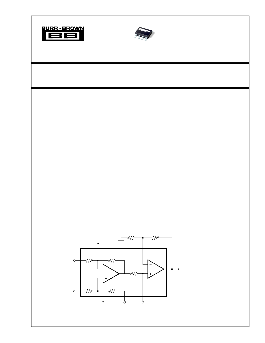
The INA145 is a precision, unity-gain difference
amplifier consisting of a precision op amp and on-
chip precision resistor network. Two external resistors
set the gain from 1V/V to 1000V/V. The input com-
mon-mode voltage range extends beyond the positive
and negative rails.
On-chip precision resistors are laser-trimmed to achieve
accurate gain and high common-mode rejection. Ex-
cellent TCR tracking of these resistors assures contin-
ued high precision over temperature.
The INA145 is available in the SO-8 surface-mount
package specified for the extended industrial tempera-
ture range, ≠40
∞
C to +85
∞
C.
FEATURES
q
DIFFERENTIAL GAIN = 1V/V TO 1000V/V:
Set with External Resistors
q
LOW QUIESCENT CURRENT: 570
µ
A
q
WIDE SUPPLY RANGE:
Single Supply: 4.5V to 36V
Dual Supplies:
±
2.25V to
±
18V
q
HIGH COMMON-MODE VOLTAGE:
+8V at V
S
= +5V
±
28V at V
S
=
±
15V
q
LOW GAIN ERROR: 0.01%
q
HIGH CMR: 86dB
q
SO-8 PACKAGE
APPLICATIONS
q
CURRENT SHUNT MEASUREMENTS
q
SENSOR AMPLIFIER
q
DIFFERENTIAL LINE RECEIVER
q
BATTERY POWERED SYSTEMS
INA145
R
5
10k
(1%)
A1
V
IN
INA145
V
O
R
2
40k
R
1
40k
V
IN
R
3
40k
R
4
40k
R
G1
R
G
R
G2
A2
V
01
Ref
V≠
V+
G = 1
+
≠
2
5
7
4
1
8
6
3
V
O
= (V
IN
≠ V
IN
)(1 + R
G2
/R
G1
)
+
≠
SBOS120
2
Æ
INA145
The information provided herein is believed to be reliable; however, BURR-BROWN assumes no responsibility for inaccuracies or omissions. BURR-BROWN assumes
no responsibility for the use of this information, and all use of such information shall be entirely at the user's own risk. Prices and specifications are subject to change
without notice. No patent rights or licenses to any of the circuits described herein are implied or granted to any third party. BURR-BROWN does not authorize or warrant
any BURR-BROWN product for use in life support devices and/or systems.
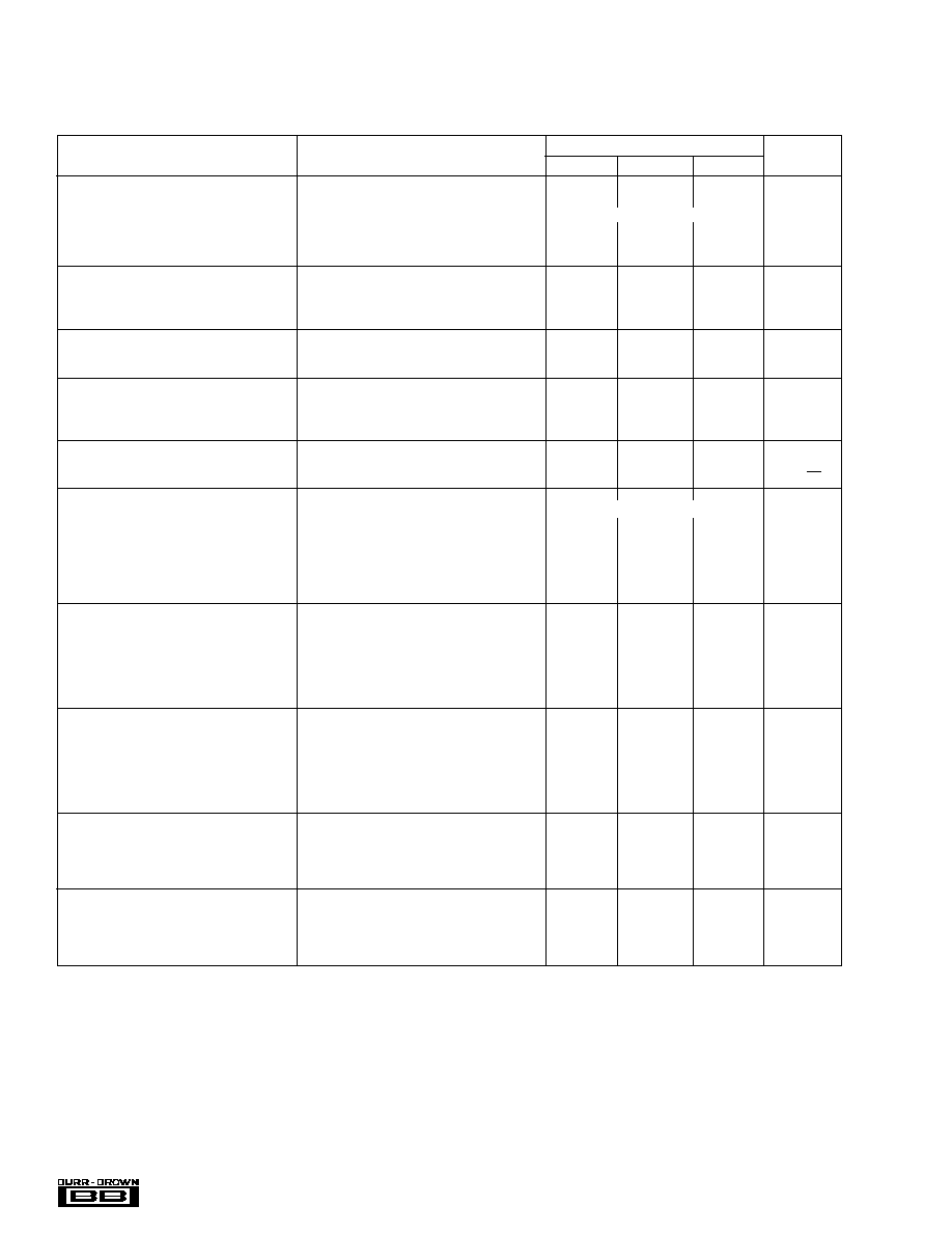
INA145UA
PARAMETER
CONDITION
MIN
TYP
MAX
UNITS
OFFSET VOLTAGE, V
O
RTI
(1, 2)
Input Offset Voltage
V
OS
V
CM
= V
O
= 0V
±
0.2
±
1
mV
vs Temperature
V
OS
/
T
See Typical Curve
vs Power Supply
PSRR
V
S
=
±
1.35V to
±
18V
±
20
±
60
µ
V/ V
vs Time
±
0.3
µ
V/mo
Offset Voltage, V
01
RTI
(1, 2)
±
0.4
mV
INPUT VOLTAGE RANGE
Common-Mode Voltage Range
V
CM
(V
IN
+) ≠ (V
IN
≠) = 0V, V
O
= 0V
2(V≠)
2(V+) ≠2
V
Common-Mode Rejection
CMRR
V
CM
= 2(V≠) to 2(V+) ≠ 2V, R
S
= 0
76
86
dB
Over Temperature
V
S
=
±
15V
70
80
dB
INPUT BIAS CURRENT
(2)
V
CM
= V
S
/2
Bias Current
I
B
±
50
nA
Offset Current
I
OS
±
5
nA
INPUT IMPEDANCE
Differential (non-inverting input)
80
k
Differential (inverting input)
27
k
Common-Mode
40
k
NOISE
RTI
(1, 3)
Voltage Noise, f = 0.1Hz to 10Hz
2
µ
Vp-p
Voltage Noise Density, f = 1kHz
e
n
90
nV/
Hz
GAIN
G = 1 to 1000
Gain Equation
G = 1 + R
G2
/ R
G1
V/ V
Initial
(1)
1
V/V
Gain Error
R
L
= 100k
, V
O
= (V≠)+0.15 to (V+)≠1, G = 1
±
0.01
±
0.1
%
vs Temperature
R
L
= 100k
, V
O
= (V≠)+0.25 to (V+)≠1, G = 1
±
2
±
10
ppm /
∞
C
R
L
= 10k
, V
O
= (V≠)+0.3 to (V+)≠1.25, G = 1
±
0.01
±
0.1
%
vs Temperature
R
L
= 10k
, V
O
= (V≠)+0.5 to (V+)≠1.25, G = 1
±
2
±
10
ppm /
∞
C
Nonlinearity
R
L
= 10k
, V
O
= (V≠)+0.3 to (V+)≠1.25, G = 1
±
0.0002
±
0.005
% of FS
FREQUENCY RESPONSE
Small Signal Bandwidth
G = 1
500
kHz
G = 10
50
kHz
Slew Rate
0.45
V/
µ
s
Settling Time, 0.1%
G = 1, 10V Step
40
µ
s
0.01%
G = 1, 10V Step
90
µ
s
Overload Recovery
50% Input Overload
40
µ
s
OUTPUT, V
O
Voltage Output
R
L
= 100k
, G = 1
(V≠) + 0.15
(V+) ≠ 1
V
Over Temperature
R
L
= 100k
, G = 1
(V≠) + 0.25
(V+) ≠ 1
V
R
L
= 10k
, G = 1
(V≠) + 0.3
(V+) ≠ 1.25
V
Over Temperature
R
L
= 10k
, G = 1
(V≠) + 0.5
(V+) ≠ 1.25
V
Short-Circuit Current
Continuous to Common
±
15
mA
Capacitive Load
Stable Operation
1000
pF
POWER SUPPLY
Specified Voltage Range, Dual Supplies
±
2.25
±
18
V
Operating Voltage Range
±
1.35
±
18
V
Quiescent Current
V
IN
= 0, I
O
= 0
±
570
±
700
µ
A
Over Temperature
±
800
µ
A
TEMPERATURE RANGE
Specified Range
≠40
+85
∞
C
Operating Range
≠55
+125
∞
C
Storage Range
≠55
+125
∞
C
Thermal Resistance
JA
150
∞
C/W
NOTES: (1) Referred to input pins (V
IN
+ and V
IN
≠), Gain = 1V/V. Specified with 10k
in feedback of A2. (2) Input offset voltage specification includes effects of amplifier's
input bias and offset currents. (3) Includes effects of input bias current noise and thermal noise contribution of resistor network.
SPECIFICATIONS: V
S
=
±
2.25V to
±
18V
Boldface limits apply over the specified temperature range, T
A
= ≠40
∞
C to +85
∞
C
At T
A
= +25
∞
C, G = 1, R
L
= 10k
connected to ground and ref pin connected to ground unless otherwise noted.
3
Æ
INA145
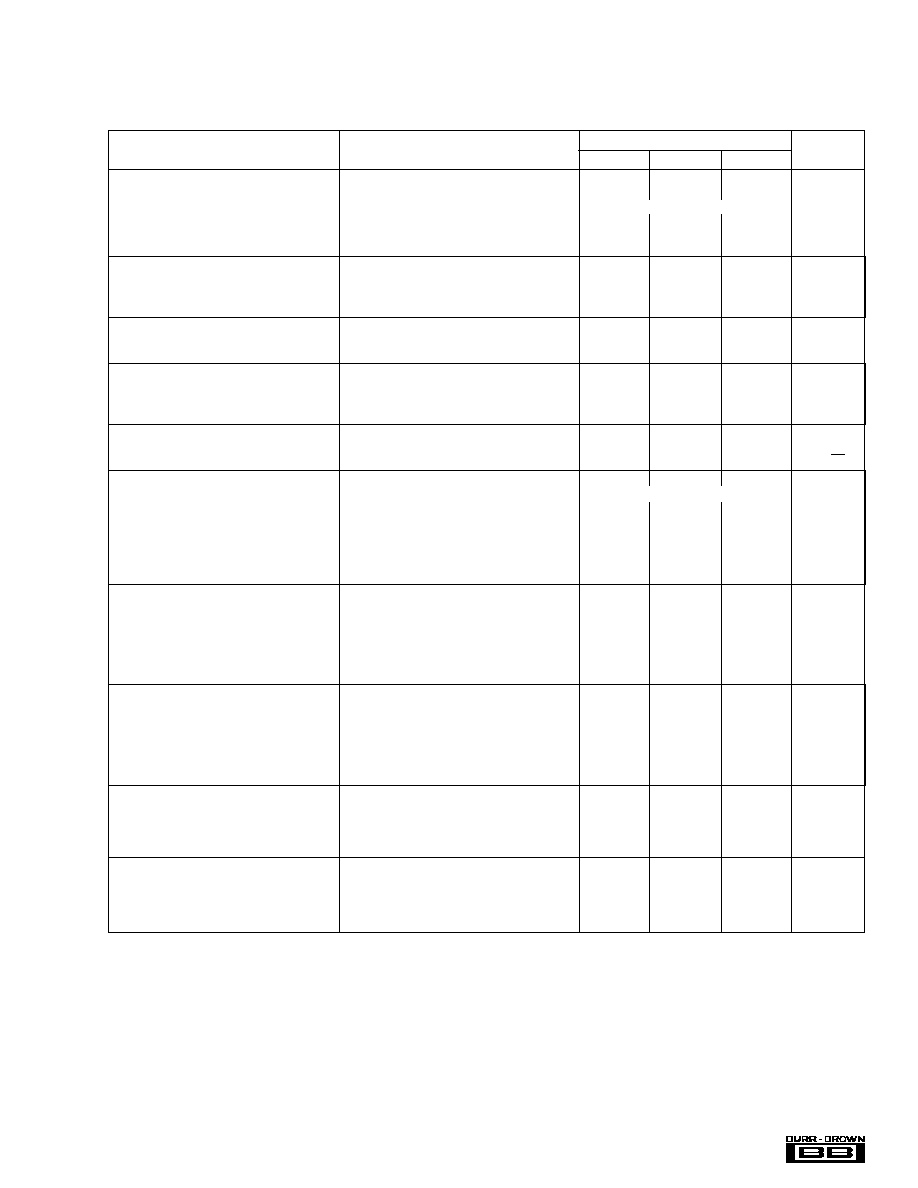
INA145UA
PARAMETER
CONDITION
MIN
TYP
MAX
UNITS
OFFSET VOLTAGE, V
O
RTI
(1, 2)
Input Offset Voltage
V
OS
V
CM
= V
O
= 2.5V
±
0.35
±
1
mV
vs Temperature
V
OS
/
T
See Typical Curve
vs Power Supply Rejection Ratio
PSRR
V
S
=
±
1.35V to
±
18V
±
20
±
60
µ
V/
∞
C
vs Time
±
0.3
µ
V/mo
Offset Voltage, V
01
RTI
(1, 2)
±
0.55
mV
INPUT VOLTAGE RANGE
Common-Mode Voltage Range
(3)
V
CM
V
IN
+ ≠ V
IN
≠ = 0V, V
O
= 2.5V
≠2.5
5.5
V
Common-Mode Rejection Ratio
CMRR
V
CM
= ≠2.5V to +5.5V, R
S
= 0
76
86
dB
Over Temperature
80
dB
INPUT BIAS CURRENT
(2)
Bias Current
I
B
±
50
nA
Offset Current
I
OS
±
5
nA
INPUT IMPEDANCE
Differential (non-inverting input)
80
k
Differential (inverting input)
27
k
Common-Mode
40
k
NOISE
RTI
(1, 4)
Voltage Noise, f = 0.1Hz to 10Hz
2
µ
Vp-p
Voltage Noise Density, f = 1kHz
e
n
90
nV/
Hz
GAIN
G = 1 to 1000
V/V
Gain Equation
G = 1 + R
G2
/ R
G1
V/V
Initial
(1)
1
V/V
Gain Error
R
L
= 100k
, V
O
= 0.15V to 4V, G = 1
±
0.01
±
0.1
%
vs Temperature
R
L
= 100k
, V
O
= 0.25V to 4V, G = 1
±
2
±
10
ppm /
∞
C
R
L
= 10k
, V
O
= 0.3V to 3.75V, G = 1
±
0.01
±
0.1
%
vs Temperature
R
L
= 10k
, V
O
= 0.5V to 3.75V, G = 1
±
2
±
10
ppm /
∞
C
Nonlinearity
R
L
= 10k
, V
O
= +0.3 to +3.75, G = 1
±
0.001
±
0.005
% of FS
FREQUENCY RESPONSE
Small Signal Bandwidth
G = 0.1
500
kHz
G = 1
50
kHz
Slew Rate
0.45
V/
µ
s
Settling Time, 0.1%
G = 1, 10V Step
40
µ
s
0.01%
G = 1, 10V Step
90
µ
s
Overload Recovery
50% Input Overload
40
µ
s
OUTPUT, V
O
Voltage Output
R
L
= 100k
, G = 1
0.15
4
V
Over Temperature
R
L
= 100k
, G = 1
0.25
4
V
R
L
= 10k
, G = 1
0.3
3.75
V
Over Temperature
R
L
= 10k
, G = 1
0.5
3.75
V
Short-Circuit Current
Continuous to Common
±
15
mA
Capacitive Load
Stable Operation
1000
pF
POWER SUPPLY
Specified Voltage Range, Single Supply
+4.5
+36
V
Operating Voltage Range
+2.7
+36
V
Quiescent Current
V
IN
= 0, I
O
= 0
550
700
µ
A
Over Temperature
800
µ
A
TEMPERATURE RANGE
Specified Range
≠40
+85
∞
C
Operating Range
≠55
+125
∞
C
Storage Range
≠55
+125
∞
C
Thermal Resistance
JA
150
∞
C/W
NOTES: (1) Referred to input pins (V
IN
+ and V
IN
≠), Gain = 1V/V. Specified with 10k
in feedback of A2. (2) Input offset voltage specification includes effects of
amplifier's input bias and offset currents. (3) Common-mode voltage range with single supply is 2(V+) ≠ 2V ≠ V
REF
to ≠V
REF
. (4) Includes effects of input current
noise and thermal noise contribution of resistor network.
SPECIFICATIONS: V
S
= +5V Single Supply
Boldface limits apply over the specified temperature range, T
A
= ≠40
∞
C to +85
∞
C
At T
A
= +25
∞
C, G = 1, R
L
= 10k
connected to ground and ref pin connected to 2.5V unless otherwise noted.
4
Æ
INA145
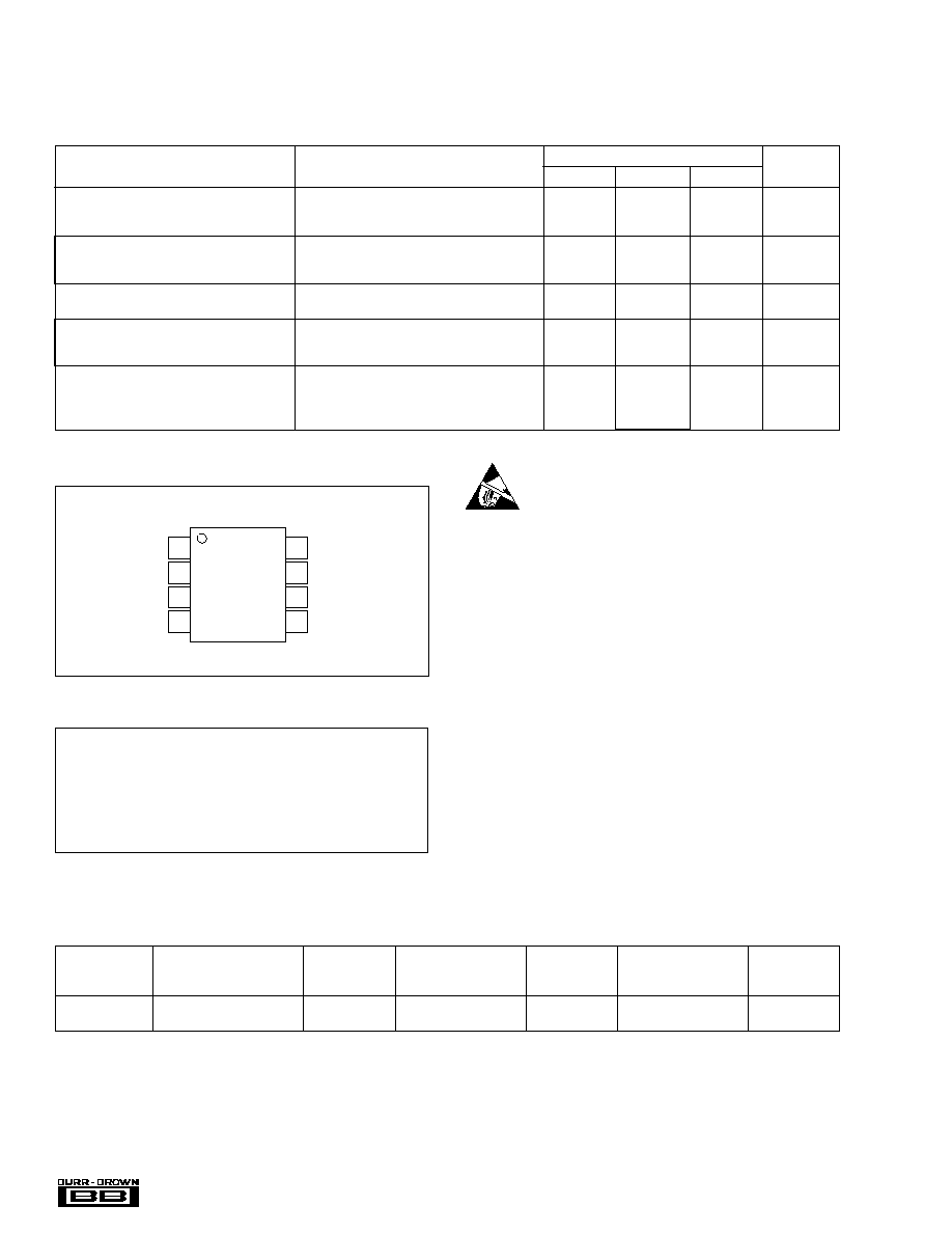
AMPLIFIER A1, A2 PERFORMANCE
Boldface limits apply over the specified temperature range, T
A
= ≠40
∞
C to +85
∞
C
At T
A
= +25
∞
C, G = 1, R
L
= 10k
connected to ground and ref pin connected to ground unless otherwise noted.
PIN CONFIGURATION
ELECTROSTATIC
DISCHARGE SENSITIVITY
This integrated circuit can be damaged by ESD. Burr-Brown
recommends that all integrated circuits be handled with
appropriate precautions. Failure to observe proper handling
and installation procedures can cause damage.
ESD damage can range from subtle performance degradation
to complete device failure. Precision integrated circuits may
be more susceptible to damage because very small parametric
changes could cause the device not to meet its published
specifications.
Supply Voltage, V+ to V≠ .................................................................... 36V
Signal Input Terminals, Voltage ........................................................
±
80V
Current .......................................................
±
1mA
Output Short Circuit (to ground) .............................................. Continuous
Operating Temperature .................................................. ≠55
∞
C to +125
∞
C
Storage Temperature ..................................................... ≠55
∞
C to +150
∞
C
Junction Temperature .................................................................... +150
∞
C
Lead Temperature (soldering, 10s) ............................................... +240
∞
C
NOTE: (1) Stresses above these ratings may cause permanent damage.
Exposure to absolute maximum conditions for extended periods may degrade
device reliability.
ABSOLUTE MAXIMUM RATINGS
(1)
Top View
SO-8
PACKAGE
SPECIFIED
DRAWING
TEMPERATURE
PACKAGE
ORDERING
TRANSPORT
PRODUCT
PACKAGE
NUMBER
RANGE
MARKING
NUMBER
(1)
MEDIA
INA145UA
SO-8
182
≠40
∞
C to +85
∞
C
INA145UA
INA145UA
Rails
"
"
"
"
"
INA145UA/2K5
Tape and Reel
NOTE: (1) Models with a slash (/) are available only in Tape and Reel in the quantities indicated (e.g., /2K5 indicates 2500 devices per reel). Ordering 2500 pieces
of "INA145UA/2K5" will get a single 2500-piece Tape and Reel.
PACKAGE/ORDERING INFORMATION
INA145UA
PARAMETER
CONDITION
MIN
TYP
MAX
UNITS
OFFSET VOLTAGE, V
O
RTI
(1, 2)
Input Offset Voltage
V
OS
V
S
=
±
15V, V
CM
= V
O
= 0V
±
0.5
mV
vs Temperature
V
OS
/
T
±
1
µ
V/
∞
C
INPUT VOLTAGE RANGE
Common-Mode Voltage Range
V
CM
V
IN
+ ≠ V
IN
≠ = 0V, V
O
= 0V
(V≠) to (V+) ≠1
V
Common-Mode Rejection Ratio
CMRR
V
CM
= (V≠) to (V+) ≠1
90
dB
OPEN-LOOP GAIN
Open Loop Gain
A
OL
110
dB
INPUT BIAS CURRENT
(2)
Bias Current
I
B
±
50
nA
Offset Current
I
OS
±
5
nA
RESISTOR AT A1 OUTPUT, V
O1
Initial
10
k
Error
±
0.2
%
Temperature Drift Coefficient
±
50
ppm/
∞
C
Ref
V
IN
V
IN
V≠
≠
+
V
O1
V+
V
O
R
G
1
2
3
4
8
7
6
5
5
Æ
INA145
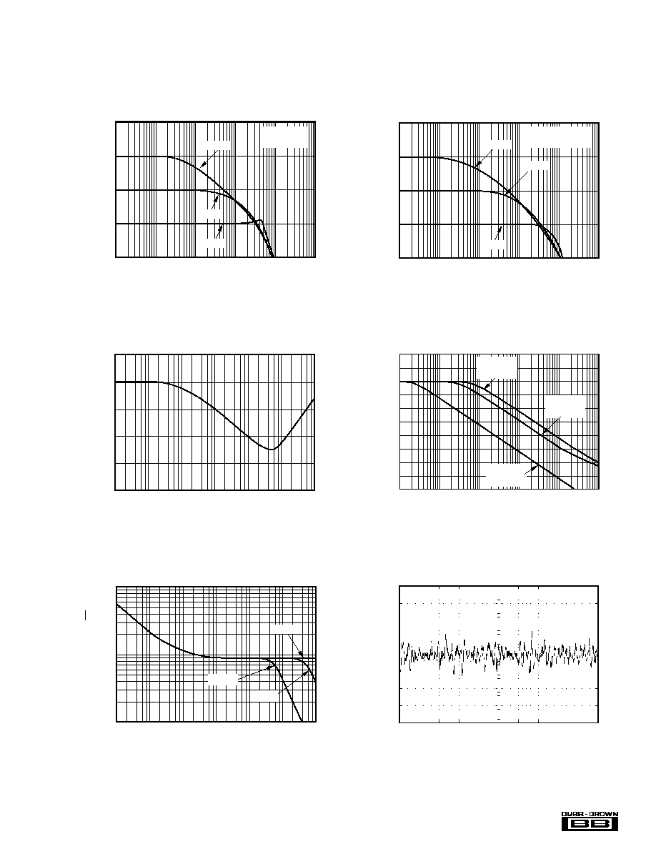
TYPICAL PERFORMANCE CURVES
At T
A
= +25
∞
C, V
S
=
±
15V, G = 1, R
L
= 10k
connected to ground and Ref pin connected to ground, unless otherwise noted.
0.1Hz to 10Hz VOLTAGE NOISE (RTI)
500ms/div
500nV/div
GAIN vs FREQUENCY
Frequency (Hz)
Voltage Gain (dB)
100
1K
10K
1M
10M
60
40
20
0
≠20
100K
G = 100
G = 10
G = 1
V
S
=
±
15V
C
L
= 200pF
10k
COMMON-MODE REJECTION vs FREQUENCY
Frequency (Hz)
Common-Mode Rejection (dB)
10
100
1k
1M
10M
100
80
60
40
20
0
10k
100k
POWER SUPPLY REJECTION vs FREQUENCY
Frequency (Hz)
Power Supply Rejection (dB)
1
10
100
10k
100k
100
80
60
40
20
0
1k
PSR+
(V
S
=
±
15V)
PSR≠
(V
S
=
±
15V)
PSR+
(V
S
= +5V)
INPUT VOLTAGE NOISE DENSITY
Frequency (Hz)
Input Voltage Noise (nV/
Hz
0.1
1
10
10k
100k
1k
100
10
100
1k
G = 1
G = 10
G = 100
GAIN vs FREQUENCY
Frequency (Hz)
Voltage Gain (dB)
100
1K
10K
1M
10M
60
40
20
0
≠20
100K
G = 100
G = 1
G = 10
V
S
=
±
15V
C
L
= 1000pF