Æ
INA148
©
1999 Burr-Brown Corporation
PDS-1579A
Printed in U.S.A.December, 1999
FEATURES
q
HIGH COMMON-MODE VOLTAGE:
+75V at V
S
= +5V
±
200V at V
S
=
±
15V
q
FIXED DIFFERENTIAL GAIN = 1V/V
q
LOW QUIESCENT CURRENT: 260
µ
A
q
WIDE SUPPLY RANGE:
Single Supply: 2.7V to 36V
Dual Supplies:
±
1.35V to
±
18V
q
LOW GAIN ERROR: 0.075% max
q
LOW NONLINEARITY: 0.002% max
q
HIGH CMR: 86dB
q
SO-8 PACKAGE
±
200V Common-Mode Voltage
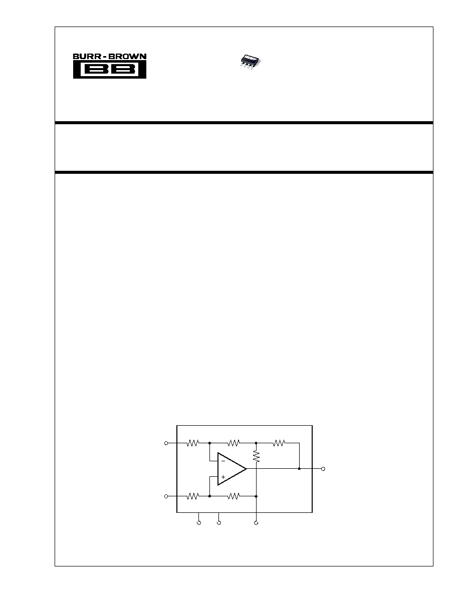
DIFFERENCE AMPLIFIER
DESCRIPTION
The INA148 is a precision, low-power, unity-gain
difference amplifier with a high common-mode input
voltage range. It consists of a monolithic precision
bipolar op amp with a thin-film resistor network.
The on-chip resistors are laser trimmed for an accu-
rate 1V/V differential gain and high common-mode
rejection. Excellent temperature tracking of the resis-
tor network maintains high gain accuracy and com-
mon-mode rejection over temperature. The INA148
will operate on single or dual supplies.
The INA148 is available in a small SO-8 surface-
mount package and it is specified for the ≠40
∞
C to
+85
∞
C extended industrial temperature range.
APPLICATIONS
q
CURRENT SHUNT MEASUREMENTS
q
DIFFERENTIAL SENSOR AMPLIFIERS
q
LINE RECEIVERS
q
BATTERY POWERED SYSTEMS
q
AUTOMOTIVE INSTRUMENTATION
q
STACKED CELL MONITORS
International Airport Industrial Park ∑ Mailing Address: PO Box 11400, Tucson, AZ 85734 ∑ Street Address: 6730 S. Tucson Blvd., Tucson, AZ 85706 ∑ Tel: (520) 746-1111
Twx: 910-952-1111 ∑ Internet: http://www.burr-brown.com/ ∑ Cable: BBRCORP ∑ Telex: 066-6491 ∑ FAX: (520) 889-1510 ∑ Immediate Product Info: (800) 548-6132
For most current data sheet and other product
information, visit www.burr-brown.com
INA148
1M
50k
52.6316k
50k
2.7778k
1M
V+
V
IN
7
3
2
6
4
1
A1
INA148
V≠
Ref
V
O
+
V
IN
≠
SBOS123
2
Æ
INA148
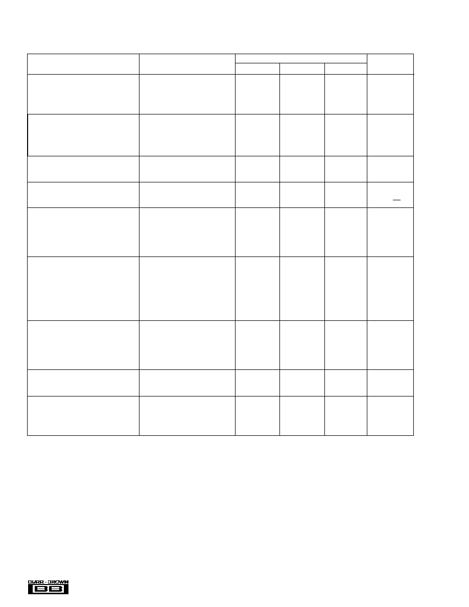
SPECIFICATIONS: V
S
=
±
5V to
±
15V Dual Supplies
At T
A
= +25
∞
C, R
L
= 10k
connected to ground and Ref pin connected to ground, unless otherwise noted.
INA148UA
PARAMETER
CONDITIONS
MIN
TYP
MAX
UNITS
OFFSET VOLTAGE (V
O
)
RTI
(1)(2)
Input Offset Voltage
V
OS
V
S
=
±
15V, V
CM
= 0V
±
1
±
5
mV
V
S
=
±
5V, V
CM
= 0V
±
1
±
5
mV
Drift
V
OS
/
T
At T
A
= ≠40
∞
C to +85
∞
C
±
10
µ
V
∞
C
vs Power Supply
PSRR
V
S
=
±
1.35V to
±
18V, V
CM
= 0V
±
50
±
400
µ
V/V
INPUT VOLTAGE RANGE
Common-Mode Voltage Range
V
CM
V
S
=
±
15V, (V
IN
+
) ≠ (V
IN
≠
) = 0V
≠200
+200
V
V
S
=
±
5V, (V
IN
+
) ≠ (V
IN
≠
) = 0V
≠100
+80
V
Common-Mode Rejection
CMRR
V
S
=
±
15V, V
CM
= ≠200V to +200V, R
S
= 0
70
86
dB
V
S
=
±
5V, V
CM
= ≠100V to +80V, R
S
= 0
70
86
dB
INPUT IMPEDANCE
Differential
2
M
Common Mode
1
M
NOISE
RTI
(1)(3)
Voltage Noise, f = 0.1Hz to 10Hz
e
n
17
µ
Vp-p
Voltage Noise Density, f = 1kHz
880
nV/
Hz
GAIN
Initial
(1)
1
V/V
Gain Error
V
O
= (V≠) + 0.5 to (V+) ≠ 1.5
±
0.01
±
0.075
%
vs Temperature
±
3
±
10
ppm/
∞
C
Nonlinearity
V
S
=
±
15V, V
O
= (V≠) + 0.5 to (V+) ≠ 1.5
±
0.001
±
0.002
% of FSR
V
S
=
±
5V, V
O
= (V≠) + 0.5 to (V+) ≠ 1.5
±
0.001
% of FSR
FREQUENCY RESPONSE
Small Signal Bandwidth
100
kHz
Slew Rate
1
V/
µ
s
Settling Time: 0.1%
V
S
=
±
15V, 10V Step
21
µ
s
0.01%
V
S
=
±
15V, 10V Step
25
µ
s
0.1%
V
S
=
±
5V, 6V Step
21
µ
s
0.01%
V
S
=
±
5V, 6V Step
25
µ
s
Overload Recovery
50% Input Overload
24
µ
s
OUTPUT (V
O
)
Voltage Output
R
L
= 100k
(V≠) + 0.25
(V+) ≠ 1
V
R
L
= 10k
(V≠) + 0.5
(V+) ≠ 1.5
V
Output Current
I
O
Short-Circiuit Current
Continuous to Common
±
13
mA
Capacitive Load
Stable Operation
10
nF
POWER SUPPLY
Operating Range, Dual Supplies
±
1.35
±
18
V
Quiescent Current
V
IN
= 0, I
O
= 0
±
260
±
300
µ
A
TEMPERATURE RANGE
Specified
≠40
85
∞
C
Operating
≠55
125
∞
C
Storage
≠55
125
∞
C
Thermal Resistance
JA
SO-8 Surface Mount
150
∞
C/W
NOTES: (1) Overall difference amplifier configuration. Referred to input pins (V
IN
+
and V
IN
≠
), gain = 1V/V (2) Input offset voltage specification includes effects of
amplifier's input bias and offset currents. (3) Includes effects of input current noise and thermal noise contribution of resistor network.
3
Æ
INA148
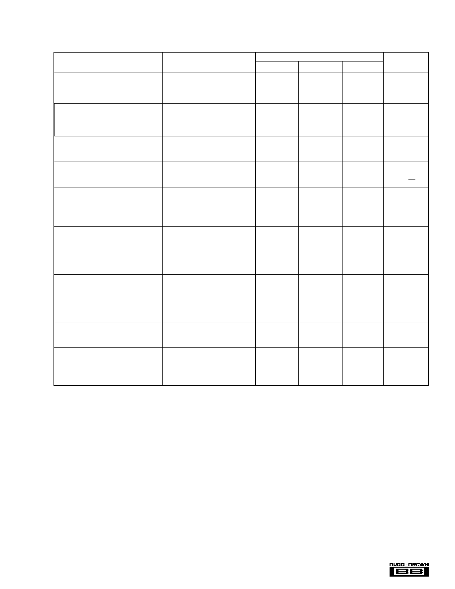
SPECIFICATIONS: V
S
= +5V Single Supply
At T
A
= +25
∞
C, R
L
= 10k
connected to V
S
/2 and Ref pin connected to V
S
/2, unless otherwise noted.
INA148UA
PARAMETER
CONDITIONS
MIN
TYP
MAX
UNITS
OFFSET VOLTAGE (V
O
)
RTI
(1)(2)
Input Offset Voltage
V
OS
V
CM
= V
S
/2
±
1
±
5
mV
Drift
V
OS
/
T
At T
A
= ≠40
∞
C to +85
∞
C
±
10
µ
V
∞
C
vs Power Supply
PSRR
V
S
= +2.7V to +36V, V
CM
= V
S
/2
±
50
±
400
µ
V/V
INPUT VOLTAGE RANGE
Common-Mode Voltage Range
V
CM
(V
IN
+
) ≠ (V
IN
≠
) = 0V, V
REF
= 0.25V
≠4
+75
V
(V
IN
+
) ≠ (V
IN
≠
) = 0V, V
REF
= V
S
/2
≠47.5
+32.5
V
Common-Mode Rejection
CMRR
V
CM
= ≠47.5V to +32.5V, R
S
= 0
70
86
dB
INPUT IMPEDANCE
Differential
2
M
Common Mode
1
M
NOISE
RTI
(1)(3)
Voltage Noise, f = 0.1Hz to 10Hz
e
n
17
µ
Vp-p
Voltage Noise Density, f = 1kHz
880
nV/
Hz
GAIN
Initial
(1)
1
V/V
Gain Error
V
O
= +0.5V to +3.5V
±
0.01
±
0.075
%
vs Temperature
±
3
±
10
ppm/
∞
C
Nonlinearity
V
O
= +0.5V to +3.5V
±
0.001
% of FSR
FREQUENCY RESPONSE
Small Signal Bandwidth
100
kHz
Slew Rate
1
V/
µ
s
Settling Time: 0.1%
V
S
= +5V, 3V Step
21
µ
s
0.01%
V
S
= +5V, 3V Step
25
µ
s
Overload Recovery
50% Input Overload
13
µ
s
OUTPUT (V
O
)
Voltage Output
R
L
= 100k
(V≠) + 0.25
(V+) ≠ 1
V
R
L
= 10k
(V≠) + 0.5
(V+) ≠ 1.5
V
Output Current
I
O
Short-Circiuit Current
Continuous to Common
±
8
mA
Capacitive Load
Stable Operation
10
nF
POWER SUPPLY
Operating Range, Single Supply
+2.7
+36
V
Quiescent Current
V
IN
= 0, I
O
= 0
260
300
µ
A
TEMPERATURE RANGE
Specified
≠40
85
∞
C
Operating
≠55
125
∞
C
Storage
≠55
125
∞
C
Thermal Resistance
JA
SO-8 Surface Mount
150
∞
C/W
NOTES: (1) Overall difference amplifier configuration. Referred to input pins (V
IN
+
and V
IN
≠
), gain = 1V/V (2) Input offset voltage specification includes effects of
amplifier's input bias and offset currents. (3) Includes effects of input current noise and thermal noise contribution of resistor network.
4
Æ
INA148
ELECTROSTATIC
DISCHARGE SENSITIVITY
This integrated circuit can be damaged by ESD. Burr-Brown
recommends that all integrated circuits be handled with
appropriate precautions. Failure to observe proper handling
and installation procedures can cause damage.
ESD damage can range from subtle performance degradation
to complete device failure. Precision integrated circuits may
be more susceptible to damage because very small parametric
changes could cause the device not to meet its published
specifications.
The information provided herein is believed to be reliable; however, BURR-BROWN assumes no responsibility for inaccuracies or omissions. BURR-BROWN assumes
no responsibility for the use of this information, and all use of such information shall be entirely at the user's own risk. Prices and specifications are subject to change
without notice. No patent rights or licenses to any of the circuits described herein are implied or granted to any third party. BURR-BROWN does not authorize or warrant
any BURR-BROWN product for use in life support devices and/or systems.
Supply Voltage, V+ to V≠ .................................................................... 36V
Signal Input Terminals, Continuous ................................................
±
200V
Peak (0.1s) ...............................................
±
500V
Output Short Circuit to GND Duration .................................... Continuous
Operating Temperature .................................................. ≠55
∞
C to +125
∞
C
Storage Temperature ..................................................... ≠55
∞
C to +125
∞
C
Junction Temperature .................................................................... +150
∞
C
Lead Temperature (soldering, 10s) ............................................... +300
∞
C
NOTE: (1) Stresses above these ratings may cause permanent damage.
Exposure to absolute maximum conditions for extended periods may degrade
device reliability. These are stress ratings only, and functional operation of the
device at these or any other conditions beyond those specified is not implied.
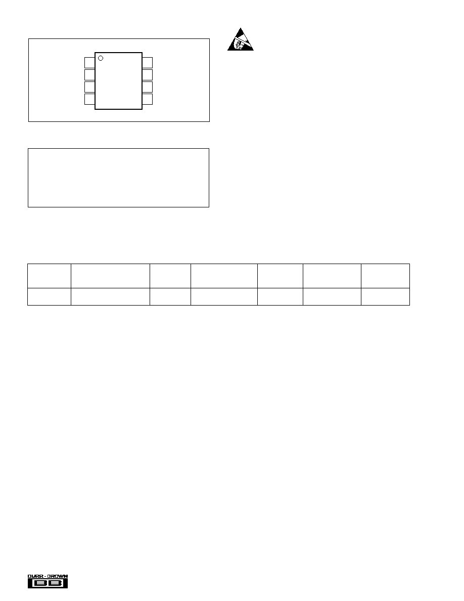
ABSOLUTE MAXIMUM RATINGS
(1)
PACKAGE
SPECIFIED
DRAWING
TEMPERATURE
PACKAGE
ORDERING
TRANSPORT
PRODUCT
PACKAGE
NUMBER
RANGE
MARKING
NUMBER
(1)
MEDIA
INA148UA
SO-8
182
≠40
∞
C to +85
∞
C
INA148UA
INA148UA
Rails
"
"
"
"
"
INA148UA/2K5
Tape and Reel
NOTE: (1) Models with a slash (/) are available only in Tape and Reel in the quantities indicated (e.g., /2K5 indicates 2500 devices per reel). Ordering 2500 pieces
of "INA148UA/2K5" will get a single 2500-piece Tape and Reel.
PACKAGE/ORDERING INFORMATION
PIN CONFIGURATION
TOP VIEW
SO-8
Ref
≠In
+In
V≠
NC
V+
Out
NC
1
2
3
4
8
7
6
5
5
Æ
INA148
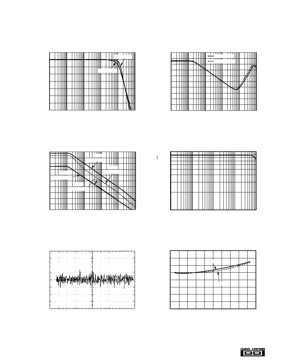
TYPICAL PERFORMANCE CURVES
At T
A
= +25
∞
C, V
S
=
±
15V, R
L
= 10k
to common, and V
REF
= 0V, unless otherwise noted.
5
0
≠5
≠10
≠20
≠25
≠30
≠35
10
100
1k
10k
100k
1M
Voltage Gain (dB)
Frequency (Hz)
GAIN vs FREQUENCY
V
S
=
±
1.35V
V
S
=
±
15V
100
80
60
40
20
0
10
100
1k
10k
100k
1M
Voltage Gain (dB)
Frequency (Hz)
COMMON-MODE REJECTION vs FREQUENCY
= V
S
=
±
15V
= V
S
=
±
1.35V
110
100
90
80
70
60
50
40
30
20
10
1
10
100
1k
10k
100K
Power Supply Rejection (dB)
Frequency (Hz)
POWER SUPPLY REJECTION vs FREQUENCY
PSR+
(V
S
=
±
18V)
PSR+
(V
S
=
±
1.35V)
PSR≠
(V
S
=
±
18V)
PSR≠
(V
S
=
±
1.35V)
800
1k
600
400
200
100
10
100
1k
10k
100k
INPUT VOLTAGE NOISE SPECTRAL DENSITY
Input Noise Spectral Density (nV/
Hz)
Frequency (Hz)
290
280
270
260
250
240
230
220
210
≠60
≠40
≠20
0
20
40
60
80
100
120
140
Temperature (
∞
C)
I
Q
(
µ
A)
QUIESCENT CURRENT vs TEMPERATURE
V
S
=
±
2.5V
V
S
=
±
15V
1s/div
5
µ
V/div
VOLTAGE NOISE (RTI)
0.1Hz to 10Hz