 | –≠–ª–µ–∫—Ç—Ä–æ–Ω–Ω—ã–π –∫–æ–º–ø–æ–Ω–µ–Ω—Ç: INA166UA | –°–∫–∞—á–∞—Ç—å:  PDF PDF  ZIP ZIP |
INA166
Copyright © 2000, Texas Instruments Incorporated
SBOS178
Printed in U.S.A. December, 2000
Low-Noise, Low-Distortion, G = 2000
INSTRUMENTATION AMPLIFIER
DESCRIPTION
The INA166 is a very low-noise, low-distortion, mon-
olithic instrumentation amplifier. Its current-feedback
circuitry achieves very wide bandwidth and excellent
dynamic response over a wide range of gain. It is ideal
for low-level signals such as microphones or hydro-
phones. Many industrial, instrumentation, and medical
applications also benefit from its low noise and wide
bandwidth.
APPLICATIONS
q
MOVING-COIL TRANSDUCER AMPLIFIERS
q
DIFFERENTIAL RECEIVERS
q
BRIDGE TRANSDUCER AMPLIFIERS
q
MICROPHONE AND HYDROPHONE
PREAMPS
www.ti.com
FEATURES
q
LOW NOISE: 1.3nV/
Hz at 1kHz
q
LOW THD+N: 0.09% at 1kHz
q
WIDE BANDWIDTH: 450kHz
q
WIDE SUPPLY RANGE:
±
4.5V to
±
18V
q
HIGH CMR: > 100dB
q
GAIN SET WITH EXTERNAL RESISTOR
q
SO-14 SURFACE-MOUNT PACKAGE
INA166
Unique distortion cancellation circuitry reduces dis-
tortion to extremely low levels, even in high gain.
The INA166 provides near-theoretical noise perfor-
mance for 200
source impedance. Its differential
input, low noise, and low distortion provide superior
performance as a low-level signal amplifier.
The INA166 is available in a space-saving SO-14
surface-mount package, specified for operation over
the ≠40
∞
C to +85
∞
C temperature range.
A1
A2
A3
6k
60k
Sense
8
9
10
14
11
6
4
3
12
5
6k
60k
V
IN
≠
+
V
IN
30.3
1
V
O
2
V
O
1
V+
V≠
INA166
G = 2000
3k
3k
V
O
Ref

INA166
2
SBOS178
INA166UA
PARAMETER
CONDITIONS
MIN
TYP
MAX
UNITS
GAIN
Gain Error
±
0.3
±
1
%
Gain Temp Drift Coefficient
±
10
ppm/
∞
C
Nonlinearity
±
0.005
% of FS
INPUT REFERRED NOISE
Voltage Noise
R
SOURCE
= 0
f
O
= 1kHz
1.3
nV/
Hz
f
O
= 100Hz
1.6
nV/
Hz
f
O
= 10Hz
2
nV/
Hz
Current Noise
f
O
= 1kHz
0.8
pA/
Hz
INPUT OFFSET VOLTAGE
Input Offset Voltage
V
CM
= V
OUT
= 0V
±
50
±
250
µ
V
vs Temperature
T
A
= T
MIN
to T
MAX
±
2.5
µ
V/
∞
C
vs Power Supply
V
S
=
±
4.5V to
±
18V
±
1
±
3
µ
V/V
INPUT VOLTAGE RANGE
Common-Mode Voltage Range
V
IN
+
≠ V
IN
≠
= 0V
(V+) ≠ 4
(V+) ≠ 3
V
V
IN
+
≠ V
IN
≠
= 0V
(V≠) + 4
(V≠) + 3
V
Common-Mode Rejection
V
CM
=
±
1V, R
SRC
= 0
100
120
dB
INPUT BIAS CURRENT
Initial Bias Current
2.5
12
µ
A
vs Temperature
15
nA/
∞
C
Initial Offset Current
0.1
1
µ
A
vs Temperature
0.5
nA/
∞
C
INPUT IMPEDANCE
Differential
60
2
M
pF
Common-Mode
60
2
M
pF
DYNAMIC RESPONSE
Bandwidth, Small Signal, ≠3dB
450
kHz
Slew Rate
15
V/
µ
s
THD+Noise, f = 1kHz
0.09
%
Settling Time, 0.1%
5V Step
2.5
µ
s
0.01%
5V Step
3.5
µ
s
Overload Recovery
50% Overdrive
1
µ
s
OUTPUT
Voltage
R
L
= 2k
to Ground
(V+) ≠ 2
(V+) ≠ 1.8
V
(V≠) + 2
(V≠) + 1.8
V
Load Capacitance Stability
1000
pF
Short-Circuit Current
Continuous-to-Common
±
60
mA
POWER SUPPLY
Rated Voltage
±
5
V
Voltage Range
±
4.5
±
18
V
Current, Quiescent
I
O
= 0mA
±
10
±
12
mA
TEMPERATURE RANGE
Specification
≠40
+85
∞
C
Operating
≠40
+125
∞
C
Thermal Resistance,
JA
100
∞
C/W
SPECIFICATIONS: V
S
=
±
5V
T
A
= +25
∞
C and at rated supplies, V
S
=
±
5V, R
L
= 2k
connected to ground, G = 2000, unless otherwise noted.
INA166
3
SBOS178
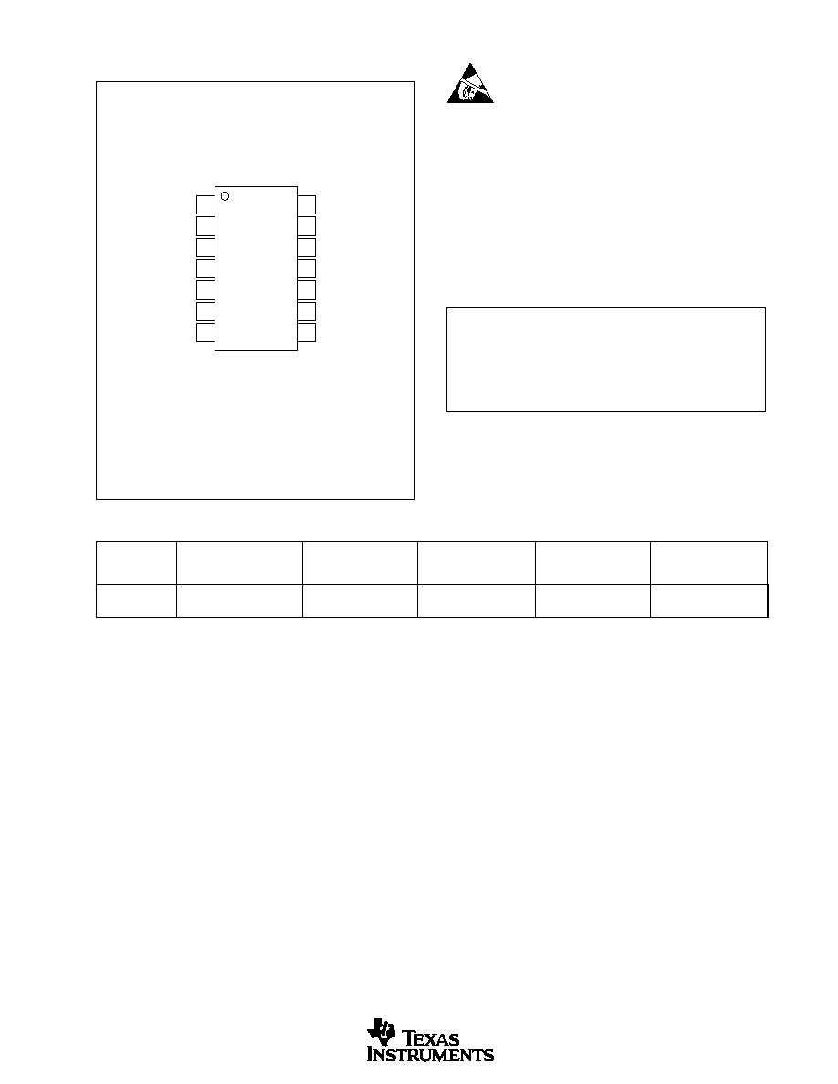
PACKAGE
DRAWING
PACKAGE
ORDERING
TRANSPORT
PRODUCT
PACKAGE
NUMBER
MARKING
NUMBER
(1)
MEDIA
INA166UA
SO-14 Surface Mount
235
INA166UA
INA166UA
Rails
"
"
"
"
INA166UA/2K5
Tape and Reel
NOTE: (1) Models with a slash (/) are available only in Tape and Reel in the quantities indicated (e.g., /2K5 indicates 2500 devices per reel). Ordering 2500 pieces
of "INA166UA/2K5" will get a single 2500-piece Tape and Reel.
ELECTROSTATIC
DISCHARGE SENSITIVITY
This integrated circuit can be damaged by ESD. Burr-Brown
recommends that all integrated circuits be handled with
appropriate precautions. Failure to observe proper handling
and installation procedures can cause damage.
ESD damage can range from subtle performance degradation
to complete device failure. Precision integrated circuits may
be more susceptible to damage because very small parametric
changes could cause the device not to meet its published
specifications.
Power Supply Voltage .......................................................................
±
18V
Signal Input Terminals, Voltage
(2)
.................. (V≠) ≠ 0.5V to (V+) + 0.5V
Current
(2)
.................................................... 10mA
Output Short-Circuit to Ground ............................................... Continuous
Operating Temperature .................................................. ≠55
∞
C to +125
∞
C
Storage Temperature ..................................................... ≠55
∞
C to +125
∞
C
Junction Temperature .................................................................... +150
∞
C
Lead Temperature (soldering, 10s) ............................................... +300
∞
C
NOTES: (1) Stresses above these ratings may cause permanent damage.
Exposure to absolute maximum conditions for extended periods may degrade
device reliability. These are stress ratings only, and functional operation of the
device at these or any other conditions beyond those specified is not implied.
(2) Input terminals are diode-clamped to the power-supply rails. Input signals
that can swing more than 0.5V beyond the supply rails should be current
limited to 10mA or less.
ABSOLUTE MAXIMUM RATINGS
(1)
PACKAGE/ORDERING INFORMATION
PIN CONFIGURATION
Top View
V
O
2
NC
GS2
V+
Ref
V
O
Sense
V
O
1
NC
GS1
V
IN
V
IN
V≠
NC
SO-14
NC = No Internal Connection
14
13
12
11
10
9
8
1
2
3
4
5
6
7
+
≠
INA166
4
SBOS178
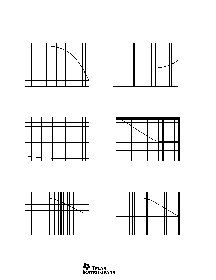
TYPICAL PERFORMANCE CURVES
At T
A
= +25
∞
C, V
S
=
±
5V, R
L
= 2k
, C
L
= 50pF, G = 2000, unless otherwise noted.
GAIN vs FREQUENCY
Gain (dB)
70
60
50
40
30
20
10
0
Frequency (Hz)
10k
100k
1M
10M
100
1k
10k
100k
1
0.1
0.01
THD+N (%)
THD+N vs FREQUENCY
Frequency (Hz)
V
O
= 5Vrms
R
L
= 10k
NOISE VOLTAGE (RTI) vs FREQUENCY
Frequency (Hz)
10
100
1k
10k
100
10
1
Noise (RTI) (nV/
Hz)
CURRENT NOISE SPECTRAL DENSITY
10.0
Current Noise Density (pA/
Hz)
1
10
100
1k
10k
Frequency (Hz)
0.1
1
CMR vs FREQUENCY
Input Referred CMR (dB)
140
120
100
80
60
40
20
0
Frequency (Hz)
10
1M
100
1k
10k
100k
POWER-SUPPLY REJECTION
vs FREQUENCY
Power-Supply Rejection (dB)
140
120
100
80
60
40
20
0
Frequency (Hz)
1
1M
10
100
1k
10k
100k
INA166
5
SBOS178
TYPICAL PERFORMANCE CURVES
(Cont.)
At T
A
= +25
∞
C, V
S
=
±
5V, R
L
= 2k
, C
L
= 50pF, G = 2000, unless otherwise noted.
OUTPUT VOLTAGE SWING vs OUTPUT CURRENT
V+
(V+)≠2
(V+)≠4
(V+)≠6
(V≠)+6
(V≠)+4
(V≠)+2
V≠
0
10
20
30
40
50
60
Output Current (mA)
Output Voltage to Rail (V)
SMALL-SIGNAL RESPONSE
500mV/div
2.5
µ
s/div
LARGE-SIGNAL RESPONSE
5V/div
2.5
µ
s/div
INA166
6
SBOS178
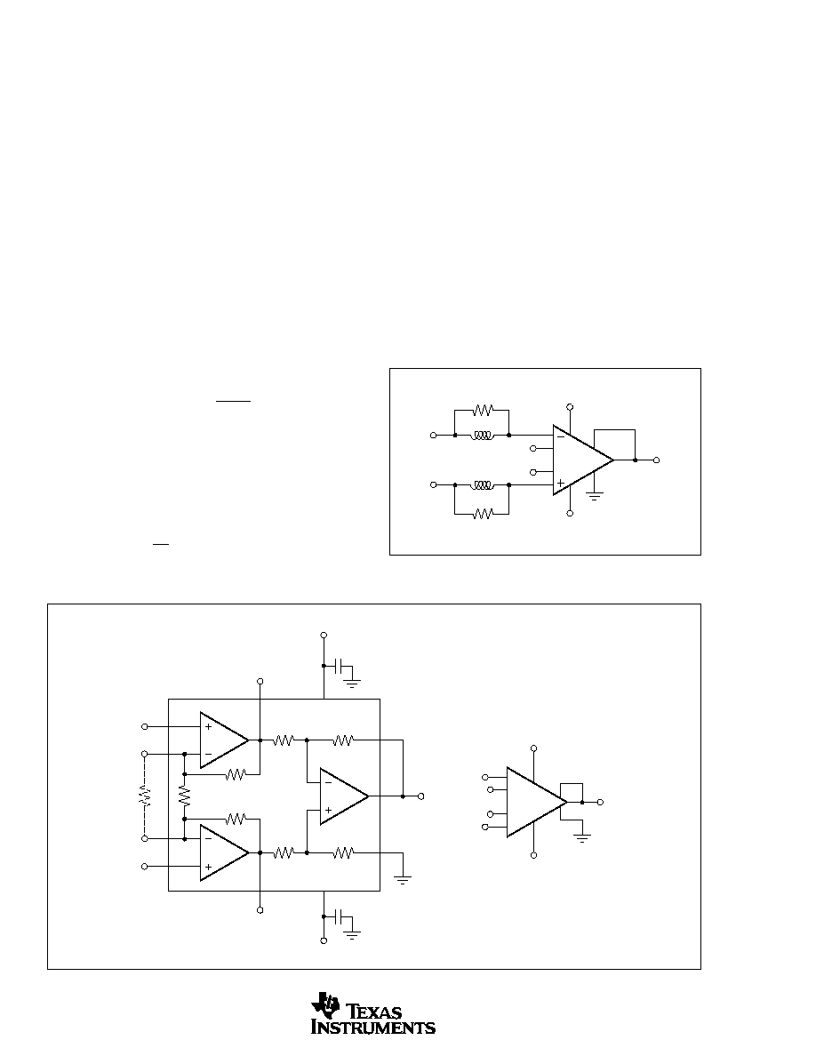
FIGURE 2. Input Stabilization Network.
APPLICATIONS INFORMATION
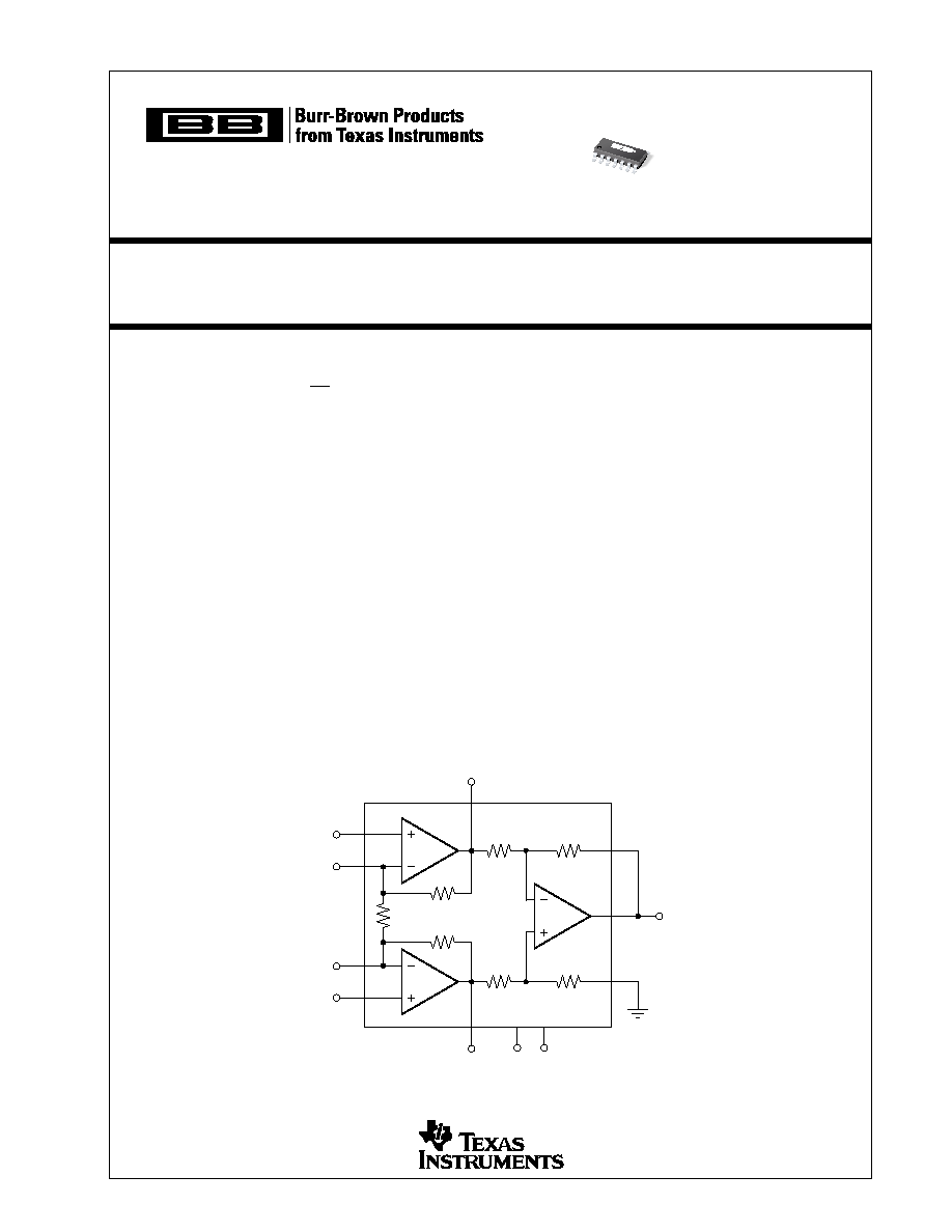
Figure 1 shows the basic connections required for operation.
Power supplies should be bypassed with 0.1
µ
F tantalum capaci-
tors near the device pins. The output Sense (pin 8) and output
Reference (pin 10) should be low-impedance connections. Re-
sistance of greater than 5
in series with these connections will
degrade the common-mode rejection of the INA166.
GAIN
Gain of the INA166 is internally set for G = 2000. Input stage
(A1, A2) gain is 200 and the output stage gain (A3) is 10.
Internal resistor values are laser trimmed for accurate ratios to
achieve excellent gain accuracy and common-mode rejection,
but absolute resistor values are approximately
±
20%. Nominal
resistor values are shown.
Although the INA166 is primarily intended for fixed-gain
applications, the gain can be increased by connecting a gain-
set resistor, R
G
, between pin 3 and pin 12 The nominal gain
will be:
G
R
G
=
+
2000
60000
Accuracy of the 60000 term in this equation is approxi-
mately
±
20%. The stability and temperature drift of R
G
contributes to the overall gain accuracy and these effects can
be inferred from this gain equation.
NOISE PERFORMANCE
The INA166 provides very low-noise with low-source im-
pedance. Its 1.3nV/
Hz voltage noise delivers near-theoreti-
cal noise performance with a source impedance of 200
.
FIGURE 1. Basic Circuit Connections.
The input stage design used to achieve this low noise, results
in relatively high input bias current and input bias current
noise. As a result, the INA166 may not provide the best
noise performance with a source impedance greater than
10k
. For source impedance greater than 10k
, other in-
strumentation amplifiers may provide improved noise per-
formance.
INPUT CONSIDERATIONS
Very low source impedance (less than 10
) can cause the
INA166 to oscillate. This depends on circuit layout, signal
source, and input cable characteristics. An input network
consisting of a small inductor and resistor, as shown in
Figure 2, can greatly reduce any tendency to oscillate. This
is especially useful if a variety of input sources are to be
connected to the INA166. Although not shown in other
figures, this network can be used as needed with all applica-
tions shown.
V+
V≠
V
O
11
6
V
IN
≠
V
IN
+
INA166
47
47
1.2
µ
H
1.2
µ
H
8
4
3
12
5
10
11
6
9
A1
A2
A3
6k
60k
Sense
8
9
10
14
6
1
11
4
3
12
5
6k
60k
V
IN
≠
+
V
IN
R
G
V+
V≠
V+
V≠
INA166
G = 2000
3k
3k
V
O
V
O
Sometimes Shown in
Simplified Form:
Ref
0.1
µ
F
0.1
µ
F
INA166
NOTE: Gain is internally set to G = 2000.
R
G
can be used to increase gain. See text.
30.3
INA166
7
SBOS178
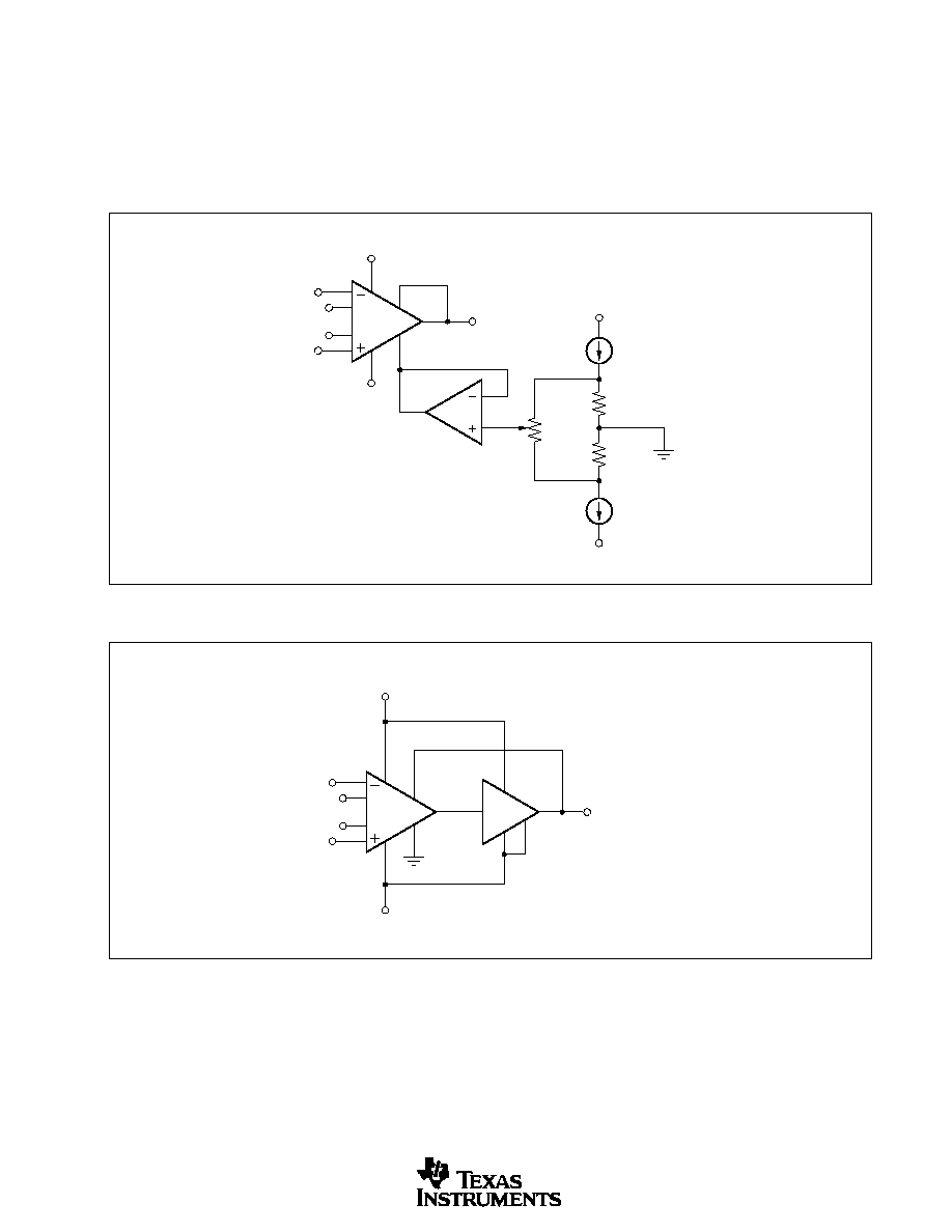
FIGURE 3. Offset Voltage Adjustment Circuit.
OFFSET VOLTAGE TRIM
A variable voltage applied to pin 10, as shown in Figure 3, can
be used to adjust the output offset voltage. A voltage applied
to pin 10 is summed with the output signal. An op amp
connected as a buffer is used to provide a low impedance at
pin 10 to assure good common-mode rejection.
FIGURE 4. Buffer for Increase Output Current.
INA166
V+
V≠
V
O
V+
150
10k
150
100
µ
A
100
µ
A
8
4
3
12
5
10
11
6
9
V≠
OPA237
OUTPUT SENSE
An output sense terminal allows greater gain accuracy in
driving the load. By connecting the sense connection at the
load, I ∑ R voltage loss to the load is included inside the
feedback loop. Current drive can be increased by connecting
a buffer amp inside the feedback loop, as shown in Figure 4.
+15V
≠15V
V
O
±
250mA
Output Drive
BW
BUF634 connected
for wide bandwidth.
8
11
6
10
9
INA166
BUF634
Sense
4
3
12
5

PACKAGING INFORMATION
ORDERABLE DEVICE
STATUS(1)
PACKAGE TYPE
PACKAGE DRAWING
PINS
PACKAGE QTY
INA166UA
ACTIVE
SOIC
D
14
58
INA166UA/2K5
ACTIVE
SOIC
D
14
2500
(1) The marketing status values are defined as follows:
ACTIVE: Product device recommended for new designs.
LIFEBUY: TI has announced that the device will be discontinued, and a lifetime-buy period is in effect.
NRND: Not recommended for new designs. Device is in production to support existing customers, but TI does not recommend using this part in
a new design.
PREVIEW: Device has been announced but is not in production. Samples may or may not be available.
OBSOLETE: TI has discontinued the production of the device.
PACKAGE OPTION ADDENDUM
www.ti.com
3-Oct-2003

IMPORTANT NOTICE
Texas Instruments Incorporated and its subsidiaries (TI) reserve the right to make corrections, modifications,
enhancements, improvements, and other changes to its products and services at any time and to discontinue
any product or service without notice. Customers should obtain the latest relevant information before placing
orders and should verify that such information is current and complete. All products are sold subject to TI's terms
and conditions of sale supplied at the time of order acknowledgment.
TI warrants performance of its hardware products to the specifications applicable at the time of sale in
accordance with TI's standard warranty. Testing and other quality control techniques are used to the extent TI
deems necessary to support this warranty. Except where mandated by government requirements, testing of all
parameters of each product is not necessarily performed.
TI assumes no liability for applications assistance or customer product design. Customers are responsible for
their products and applications using TI components. To minimize the risks associated with customer products
and applications, customers should provide adequate design and operating safeguards.
TI does not warrant or represent that any license, either express or implied, is granted under any TI patent right,
copyright, mask work right, or other TI intellectual property right relating to any combination, machine, or process
in which TI products or services are used. Information published by TI regarding third-party products or services
does not constitute a license from TI to use such products or services or a warranty or endorsement thereof.
Use of such information may require a license from a third party under the patents or other intellectual property
of the third party, or a license from TI under the patents or other intellectual property of TI.
Reproduction of information in TI data books or data sheets is permissible only if reproduction is without
alteration and is accompanied by all associated warranties, conditions, limitations, and notices. Reproduction
of this information with alteration is an unfair and deceptive business practice. TI is not responsible or liable for
such altered documentation.
Resale of TI products or services with statements different from or beyond the parameters stated by TI for that
product or service voids all express and any implied warranties for the associated TI product or service and
is an unfair and deceptive business practice. TI is not responsible or liable for any such statements.
Following are URLs where you can obtain information on other Texas Instruments products and application
solutions:
Products
Applications
Amplifiers
amplifier.ti.com
Audio
www.ti.com/audio
Data Converters
dataconverter.ti.com
Automotive
www.ti.com/automotive
DSP
dsp.ti.com
Broadband
www.ti.com/broadband
Interface
interface.ti.com
Digital Control
www.ti.com/digitalcontrol
Logic
logic.ti.com
Military
www.ti.com/military
Power Mgmt
power.ti.com
Optical Networking
www.ti.com/opticalnetwork
Microcontrollers
microcontroller.ti.com
Security
www.ti.com/security
Telephony
www.ti.com/telephony
Video & Imaging
www.ti.com/video
Wireless
www.ti.com/wireless
Mailing Address:
Texas Instruments
Post Office Box 655303 Dallas, Texas 75265
Copyright
2003, Texas Instruments Incorporated