 | –≠–ª–µ–∫—Ç—Ä–æ–Ω–Ω—ã–π –∫–æ–º–ø–æ–Ω–µ–Ω—Ç: INA169 | –°–∫–∞—á–∞—Ç—å:  PDF PDF  ZIP ZIP |
INA139
INA169
FEATURES
q
COMPLETE UNIPOLAR HIGH-SIDE
CURRENT MEASUREMENT CIRCUIT
q
WIDE SUPPLY AND COMMON-MODE RANGE
q
INA139: 2.7V to 40V
q
INA169: 2.7V to 60V
q
INDEPENDENT SUPPLY AND INPUT COMMON-
MODE VOLTAGES
q
SINGLE RESISTOR GAIN SET
q
LOW QUIESCENT CURRENT (60
µ
A typ)
q
SOT23-5 PACKAGE
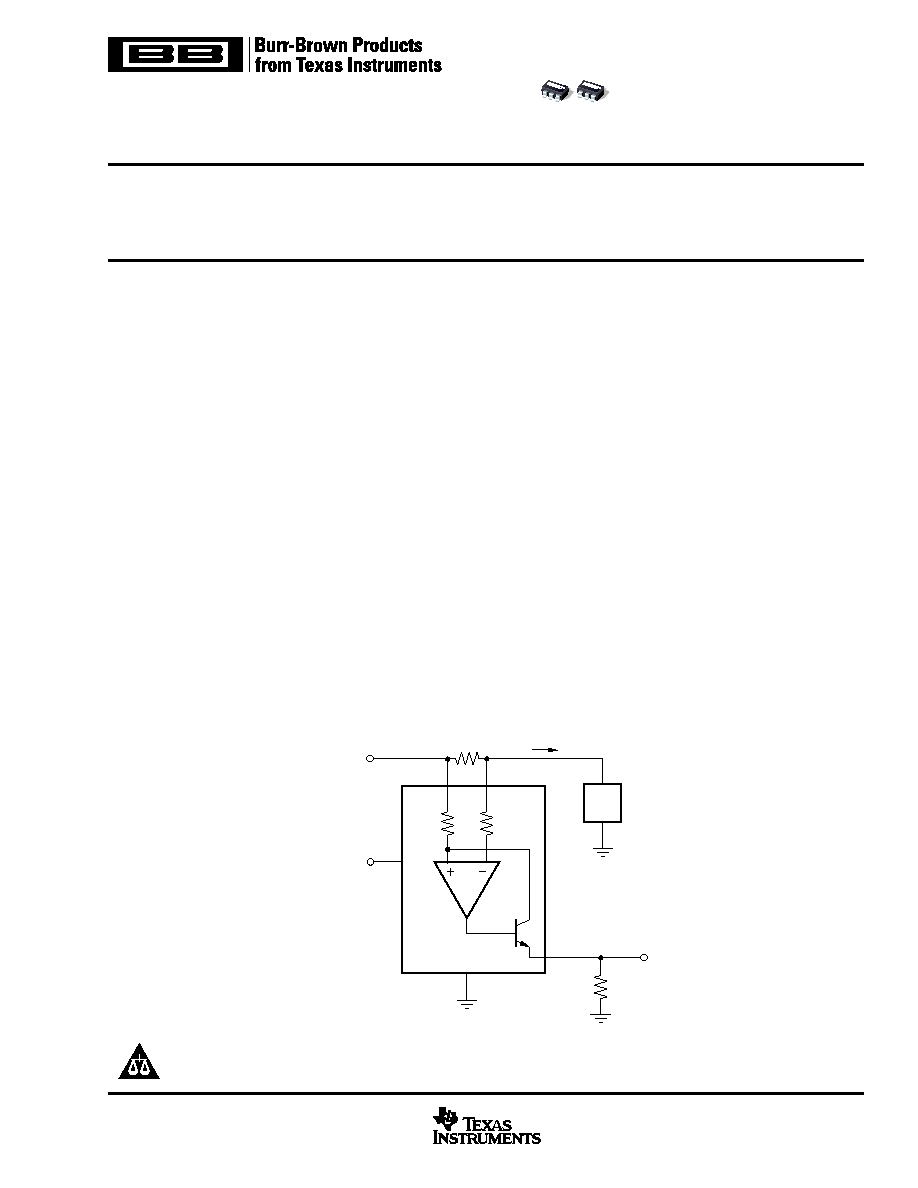
High-Side Measurement
CURRENT SHUNT MONITOR
DESCRIPTION
The INA139 and INA169 are high-side, unipolar, current
shunt monitors. Wide input common-mode voltage range,
high-speed, low quiescent current, and tiny SOT23 packag-
ing enable use in a variety of applications.
Input common-mode and power-supply voltages are inde-
pendent and can range from 2.7V to 40V for the INA139 and
2.7V to 60V for the INA169. Quiescent current is only 60
µ
A,
which permits connecting the power supply to either side of
the current measurement shunt with minimal error.
The device converts a differential input voltage to a current
output. This current is converted back to a voltage with an
external load resistor that sets any gain from 1 to over 100.
Although designed for current shunt measurement, the cir-
cuit invites creative applications in measurement and level
shifting.
Both the INA139 and INA169 are available in SOT23-5
packages and are specified for the ≠40
∞
C to +85
∞
C industrial
temperature range.
APPLICATIONS
q
CURRENT SHUNT MEASUREMENT:
Automotive, Telephone, Computers
q
PORTABLE AND BATTERY-BACKUP
SYSTEMS
q
BATTERY CHARGERS
q
POWER MANAGEMENT
q
CELL PHONES
q
PRECISION CURRENT SOURCE
R
S
2
1
OUT
GND
R
L
V
O
= I
S
R
S
R
L
/1k
Load
1k
1k
V
IN+
Up to 60V
V
IN+
V
IN≠
3
4
I
S
V+
5
SBOS181C ≠ DECEMBER 2000 ≠ REVISED JULY 2004
www.ti.com
PRODUCTION DATA information is current as of publication date.
Products conform to specifications per the terms of Texas Instruments
standard warranty. Production processing does not necessarily include
testing of all parameters.
Copyright © 2000-2004, Texas Instruments Incorporated
Please be aware that an important notice concerning availability, standard warranty, and use in critical applications of
Texas Instruments semiconductor products and disclaimers thereto appears at the end of this data sheet.

INA139, INA169
2
SBOS181C
www.ti.com
Supply Voltage, V+
INA139 ............................................................................... ≠0.3V to 60V
INA169 ............................................................................... ≠0.3V to 75V
Analog Inputs, V
IN+,
V
IN≠
INA139
Common Mode ............................................................... ≠0.3V to 60V
Differential (V
IN+
)
≠ (V
IN≠
) .................................................. ≠40V to 2V
INA169
Common Mode ............................................................... ≠0.3V to 75V
Differential (V
IN+
)
≠ (V
IN≠
) .................................................. ≠40V to 2V
Analog Output, Out .............................................................. ≠0.3V to 40V
Operating Temperature .................................................. ≠55
∞
C to +125
∞
C
Storage Temperature ..................................................... ≠65
∞
C to +125
∞
C
Junction Temperature .................................................................... +150
∞
C
Lead Temperature (soldering, 10s) ............................................... +300
∞
C
NOTE: (1) Stresses above these ratings may cause permanent damage.
Exposure to absolute maximum conditions for extended periods may degrade
device reliability. These are stress ratings only, and functional operation of the
device at these or any other conditions beyond those specified is not implied.
ABSOLUTE MAXIMUM RATINGS
(1)
PIN CONFIGURATION
Top View
SOT
OUT
GND
V
IN
V+
V
IN
1
2
3
5
4
+
≠
ELECTROSTATIC
DISCHARGE SENSITIVITY
This integrated circuit can be damaged by ESD. Texas Instru-
ments recommends that all integrated circuits be handled with
appropriate precautions. Failure to observe proper handling
and installation procedures can cause damage.
ESD damage can range from subtle performance degrada-
tion to complete device failure. Precision integrated circuits
may be more susceptible to damage because very small
parametric changes could cause the device not to meet its
published specifications.
SPECIFIED
PACKAGE
TEMPERATURE
PACKAGE
ORDERING
TRANSPORT
PRODUCT
PACKAGE-LEAD
DESIGNATOR
RANGE
MARKING
NUMBER
MEDIA, QUANTITY
INA139
SOT23-5 Surface-Mount
DBV
≠40
∞
C to +85
∞
C
E39
INA139NA/250
Tape and Reel, 250
"
"
"
"
"
INA139NA/3K
Tape and Reel, 3000
INA169
SOT23-5 Surface-Mount
DBV
≠40
∞
C to +85
∞
C
A69
INA169NA/250
Tape and Reel, 250
"
"
"
"
"
INA169NA/3K
Tape and Reel, 3000
NOTE: (1) For the most current package and ordering information, see the Package Option Addendum located at the end of this data sheet.
PACKAGE/ORDERING INFORMATION
(1)
INA139, INA169
3
SBOS181C
www.ti.com
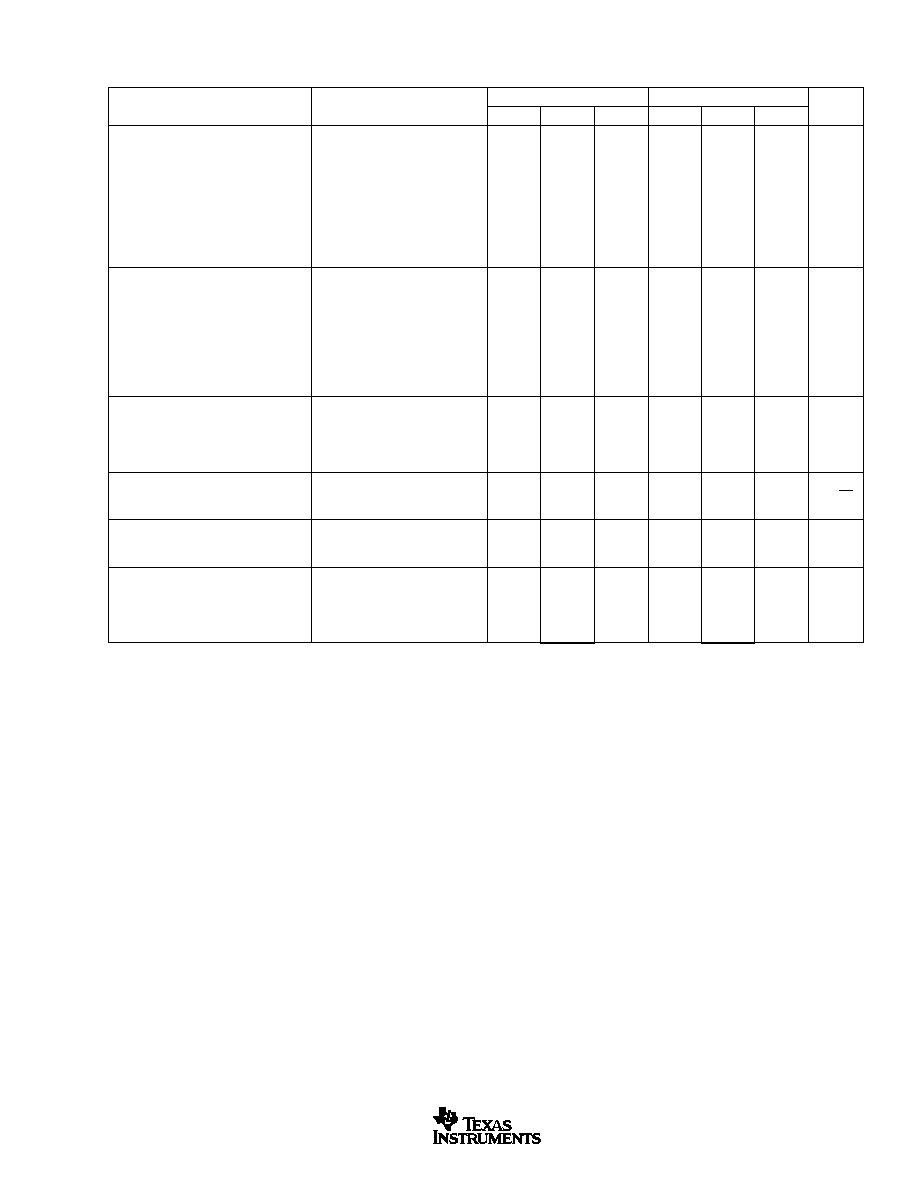
ELECTRICAL CHARACTERISTICS
At T
A
= ≠40
∞
C to +85
∞
C, V
S
= 5V, V
IN+
= 12V, and R
OUT
= 25k
, unless otherwise noted.
PARAMETER
CONDITION
MIN
TYP
MAX
MIN
TYP
MAX
UNITS
INPUT
Full-Scale Sense Voltage
V
SENSE
= (V
IN+
)
≠ (V
IN≠
)
100
500
mV
Common-Mode Input Range
2.7
40
60
V
Common-Mode Rejection
V
IN+
= 2.7V to 40V, V
SENSE
= 50mV
100
115
dB
V
IN+
= 2.7V to 60V, V
SENSE
= 50mV
100
120
dB
Offset Voltage
(1)
RTI
±
0.2
±
1
mV
vs Temperature
T
MIN
to T
MAX
1
µ
V/
∞
C
vs Power Supply, V+
V≠
= 2.7V to 40V, V
SENSE
= 50mV
0.5
10
µ
V/V
V≠
= 2.7V to 60V, V
SENSE
= 50mV
0.1
10
µ
V/V
Input Bias Current
10
uA
OUTPUT
Transconductance
V
SENSE
= 10mV
≠ 150mV
990
1000
1010
µ
A/V
vs Temperature
V
SENSE
= 100mV
10
nA/
∞
C
Nonlinearity Error
V
SENSE
= 10mV
to 150mV
±
0.01
±
0.1
%
Total Output Error
V
SENSE
= 100mV
±
0.5
±
2
%
Output Impedance
1 || 5
G
|| pF
Voltage Output
Swing to Power Supply, V+
(V+) ≠ 0.9 (V+) ≠ 1.2
V
Swing to Common Mode, V
CM
V
CM
≠ 0.6 V
CM
≠ 1.0
V
FREQUENCY RESPONSE
Bandwidth
R
OUT
= 10k
440
kHz
R
OUT
= 20k
220
kHz
Settling Time (0.1%)
5V Step, R
OUT
= 10k
2.5
µ
s
5V Step, R
OUT
= 20k
5.0
µ
s
NOISE
Output-Current Noise Density
20
pA/
Hz
Total Output-Current Noise
BW = 100kHz
7
nA RMS
POWER SUPPLY
Operating Range, V+
2.7
40
60
V
Quiescent Current
V
SENSE
= 0, I
O
= 0
60
125
µ
A
TEMPERATURE RANGE
Specification, T
MIN
to T
MAX
≠40
85
∞
C
Operating
≠55
125
∞
C
Storage
≠65
150
∞
C
Thermal Resistance
JA
200
∞
C/W
Specification same as for the INA139NA.
NOTE: (1) Defined as the amount of input voltage, V
SENSE
, to drive the output to zero.
INA139NA
INA169NA
INA139, INA169
4
SBOS181C
www.ti.com
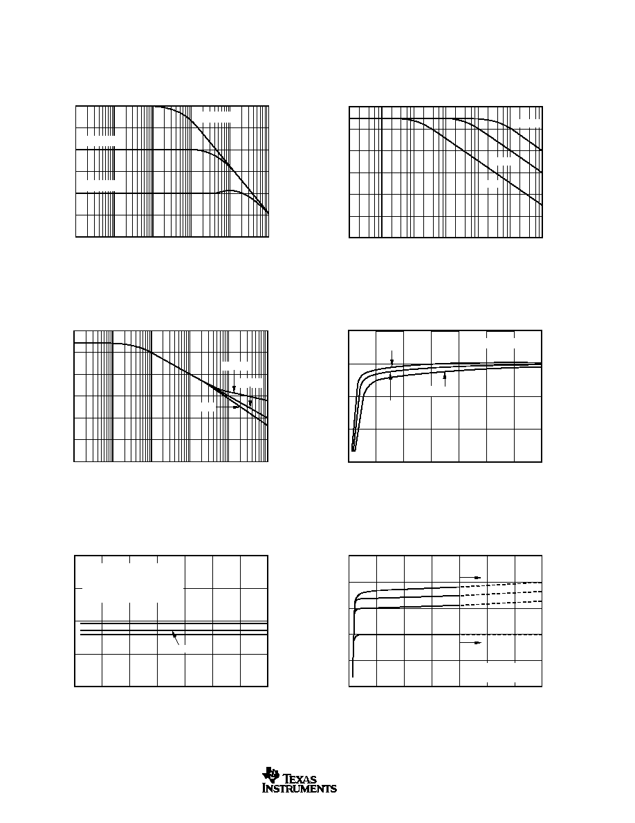
TYPICAL CHARACTERISTICS
At T
A
= +25
∞
C, V+ = 5V, V
IN+
= 12V, and R
L
= 25k
, unless otherwise noted.
40
30
20
10
0
≠10
≠20
100
1k
10k
100k
1M
10M
Gain (dB)
Frequency (Hz)
GAIN vs FREQUENCY
R
L
= 10k
R
L
= 100k
R
L
= 1k
120
100
80
60
40
20
0
0.1
1
10
100
1k
10k
Common-Mode Rejection (dB)
Frequency (Hz)
100k
G = 1
G = 10
G = 100
COMMON-MODE REJECTION vs FREQUENCY
140
120
100
80
60
40
20
1
10
100
1k
10k
100k
PSR (dB)
Frequency (Hz)
POWER-SUPPLY REJECTION vs FREQUENCY
G = 1
G = 10
G = 100
5
0
≠5
≠10
≠15
0
25
50
75
100
125
Total Output Error (%)
V
IN
(mV)
TOTAL OUTPUT ERROR vs V
IN
150
200
≠55
∞
C
+25
∞
C
+150
∞
C
V
IN
= (V
IN+
-
V
IN
-
)
2
1
0
≠1
≠2
0
10
20
30
40
50
Total Output Error (%)
Power-Supply Voltage (V)
TOTAL OUTPUT ERROR
vs POWER-SUPPLY VOLTAGE
60
70
G = 1
G = 10
G = 25
Output error is essentially
independent of both
V+ supply voltage and
input common-mode voltage.
100
80
60
40
20
0
0
10
20
30
40
50
Quiescent Current (
µ
A)
Power-Supply Voltage (V)
QUIESCENT CURRENT
vs POWER-SUPPLY VOLTAGE
60
70
+150
∞
+125
∞
+25
∞
≠55
∞
Use the INA169 with
(V+) > 40V
INA139, INA169
5
SBOS181C
www.ti.com
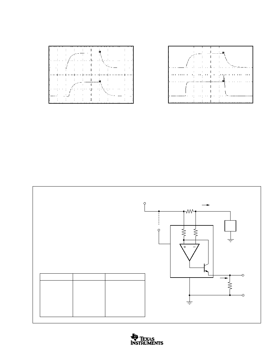
TYPICAL CHARACTERISTICS
(Cont.)
At T
A
= +25
∞
C, V+ = 5V, V
IN+
= 12V, and R
L
= 25k
, unless otherwise noted.
STEP RESPONSE
20
µ
s/div
1.5V
G = 100
0.5V
1V
G = 100
0V
STEP RESPONSE
10
µ
s/div
1V
G = 50
0V
2V
G = 10
0V
OPERATION
Figure 1 shows the basic circuit diagram for both the INA139
and the INA169. Load current, I
S
, is drawn from the supply,
V
S
, through the shunt resistor, R
S
. The voltage drop in the
shunt resistor, V
S
, is forced across R
G1
by the internal op
amp, causing current to flow into the collector of Q1. The
external resistor, R
L
, converts the output current to a voltage,
V
OUT
, at the OUT pin.
The transfer function for the INA139 is:
I
O
= g
m
(V
IN+
)
≠ (V
IN≠
)
(1)
where g
m
= 1000
µ
A/V
(2)
In the circuit of Figure 1, the input voltage, (V
IN+
)
≠ (V
IN≠
), is
equal to I
S
∑ R
S
and the output voltage, V
OUT
, is equal to
I
O
∑ R
L
. The transconductance, g
m
, of the INA139 is
1000
µ
A/V. The complete transfer function for the current
measurement amplifier in this application is:
V
OUT
= (I
S
) (R
S
) (1000
µ
A/V) (R
L
)
(3)
FIGURE 1. Basic Circuit Connections.
VOLTAGE GAIN
EXACT R
L
(
)
NEAREST 1% R
L
(
)
1
1k
1k
2
2k
2k
5
5k
4.99k
10
10k
10k
20
20k
20k
50
50k
49k
100
100k
100k
Shunt
R
S
INA139
2
1
OUT
Q1
R
L
I
O
+
V
O
≠
Load
R
G1
1k
R
G2
1k
V
IN+
V
IN≠
3
4
I
S
V+
5
NOTE: (1) Maximum V
P
and V+ voltage is 60V with the INA169.
V+ power can be
common or
indepedent of
load supply.
2.7V
(V+)
40V
(1)
V
P
Load Power Supply
+2.7V to 40V
(1)