Document Outline
- FEATURES
- APPLICATIONS
- DESCRIPTION
- ABSOLUTE MAXIMUM RATINGS
- PACKAGE/ORDERING INFORMATION
- PIN CONFIGURATION
- ELECTRICAL CHARACTERISTICS: V S =+2.7V to +5.5V
- TYPICAL CHARACTERISTICS
- APPLICATIONS INFORMATION
- OPERATING VOLTAGE
- SETTING THE GAIN
- COMMON-MODE INPUT RANGE
- REFERENCE
- INPUT BIAS CURRENT RETURN
- SHUTDOWN MODE
- RAIL-TO-RAIL OUTPUT
- OUTPUT BUFFERING
- OFFSET TRIMMING
- INPUT PROTECTION
- OFFSET VOLTAGE ERROR CALCULATION
- FEEDBACK CAPACITOR IMPROVES RESPONSE
- APPLICATION CIRCUITS
- MEDICAL ECG APPLICATIONS
- LOW-POWER, SINGLE-SUPPLY DATA ACQUISITION SYSTEMS
- PACKAGE DRAWINGS
- DGK (R-PDSO-G8) PLASTIC SMALL-OUTLINE PACKAGE
- PW (R-PDSO-G**) PLASTIC SMALL-OUTLINE PACKAGE
INA331
INA2331
SBOS215B ≠ DECEMBER 2001 ≠ REVISED APRIL 2003
DESCRIPTION
The INA331 and INA2331 are rail-to-rail output, low-power
CMOS instrumentation amplifiers that offer wide range, single-
supply operation as well as bipolar-supply operation. The
INA331 family provides low-cost, low-noise amplification of
differential signals with a low quiescent current of 415
µ
A
(dropping to 0.01
µ
A when shutdown). Returning to normal
operation within microseconds, this INA can be used for
battery or multi-channel applications.
Configured internally in a gain of 5V/V, the INA331 offers
flexibility in higher gains by choosing external resistors.
FEATURES
q
DESIGNED FOR LOW COST
q
HIGH GAIN ACCURACY: G = 5, 0.02%, 2ppm/
∞
C
q
GAIN SET WITH EXT. RESISTORS FOR > 5V/V
q
LOW OFFSET VOLTAGE:
±
250
µ
V
q
HIGH CMRR: 94dB DC, 50dB at 45kHz
q
LOW BIAS CURRENT: 0.5pA
q
BANDWIDTH, SLEW RATE: 2.0MHz, 5V/
µ
s
q
RAIL-TO-RAIL OUTPUT SWING: (V+) ≠ 0.02V
q
WIDE TEMPERATURE RANGE: ≠55
∞
C to +125
∞
C
q
LOW QUIESCENT CURRENT: 490
µ
A max/chan
q
SHUT DOWN: 0.01
µ
A
q
MSOP-8 SINGLE AND TSSOP-14 DUAL PACKAGES
Copyright © 2001-2003, Texas Instruments Incorporated
Low-Power, Single-Supply, CMOS
INSTRUMENTATION AMPLIFIERS
Please be aware that an important notice concerning availability, standard warranty, and use in critical applications of
Texas Instruments semiconductor products and disclaimers thereto appears at the end of this data sheet.
APPLICATIONS
q
INDUSTRIAL SENSOR AMPLIFIERS:
Bridge, RTD, Thermocouple, Position
q
PHYSIOLOGICAL AMPLIFIERS:
ECG, EEG, EMG
q
A/D CONVERTER SIGNAL CONDITIONING
q
DIFFERENTIAL LINE RECEIVERS WITH GAIN
q
FIELD UTILITY METERS
q
PCMCIA CARDS
q
AUDIO AMPLIFIERS
q
COMMUNICATION SYSTEMS
q
TEST EQUIPMENT
q
AUTOMOTIVE INSTRUMENTATION
The INA331 rejects line noise and its harmonics, because
common-mode error remains low even at higher frequencies.
High bandwidth and slew rate makes the INA331 ideal for
directly driving sampling Analog-to-Digital (A/D) converters
as well as general-purpose applications.
With high precision, low cost, and small packages, the
INA331 outperforms discrete designs.
Additionally, because they are specified for wide temperature
range of ≠55
∞
C to +125
∞
C and operating range of ≠65
∞
C to
+150
∞
C, they can be used in demanding industrial and
automotive environments.
A2
A1
A3
40k
V
REF
V
IN
≠
V
IN
+
10k
10k
Shutdown
V+
V
OUT
G = 5 + (5R
2
/R
1
)
V≠
R
2
R
1
R
G
40k
Ch A
INA2331
INA331
Ch B
Æ
INA2
331
INA3
31
PRODUCTION DATA information is current as of publication date.
Products conform to specifications per the terms of Texas Instruments
standard warranty. Production processing does not necessarily include
testing of all parameters.
www.ti.com
INA331, INA2331
SBOS215B
2
www.ti.com
Supply Voltage, V+ to V≠ .................................................................... 7.5V
Signal Input Terminals, Voltage
(2)
..................... (V≠) ≠ 0.5V to (V+) + 0.5V
Current
(2)
..................................................... 10mA
Output Short-Circuit
(3)
.............................................................. Continuous
Operating Temperature .................................................. ≠55
∞
C to +125
∞
C
Storage Temperature ...................................................... ≠65
∞
C to +150
∞
C
Junction Temperature ...................................................................... 150
∞
C
Lead Temperature (soldering, 10s) ................................................. 300
∞
C
NOTES: (1) Stresses above these ratings may cause permanent damage.
Exposure to absolute maximum conditions for extended periods may degrade
device reliability. (2) Input terminals are diode-clamped to the power-supply rails.
Input signals that can swing more than 0.5V beyond the supply rails should be
current limited to 10mA or less. (3) Short-circuit to ground, one amplifier per
package.
ABSOLUTE MAXIMUM RATINGS
(1)
ELECTROSTATIC
DISCHARGE SENSITIVITY
This integrated circuit can be damaged by ESD. Texas Instru-
ments recommends that all integrated circuits be handled with
appropriate precautions. Failure to observe proper handling
and installation procedures can cause damage.
ESD damage can range from subtle performance degradation
to complete device failure. Precision integrated circuits may be
more susceptible to damage because very small parametric
changes could cause the device not to meet its published
specifications.
SPECIFIED
PACKAGE
TEMPERATURE
PACKAGE
ORDERING
TRANSPORT
PRODUCT
PACKAGE-LEAD
DESIGNATOR
(1)
RANGE
MARKING
NUMBER
MEDIA, QUANTITY
Single
INA331IDGK
MSOP-8
DGK
≠55
∞
C to +125
∞
C
C31
INA331IDGKT
Tape and Reel, 250
"
"
"
"
"
INA331IDGKR
Tape and Reel, 2500
INA331AIDGK
MSOP-8
DGK
≠55
∞
C to +125
∞
C
C31
INA331AIDGKT
Tape and Reel, 250
"
"
"
"
"
INA331AIDGKR
Tape and Reel, 2500
Dual
INA2331AIPW
TSSOP-14
PW
≠55
∞
C to +125
∞
C
2331A
INA2331AIPWT
Tape and Reel, 250
"
"
"
"
"
INA2331AIPWR
Tape and Reel, 2500
PACKAGE/ORDERING INFORMATION
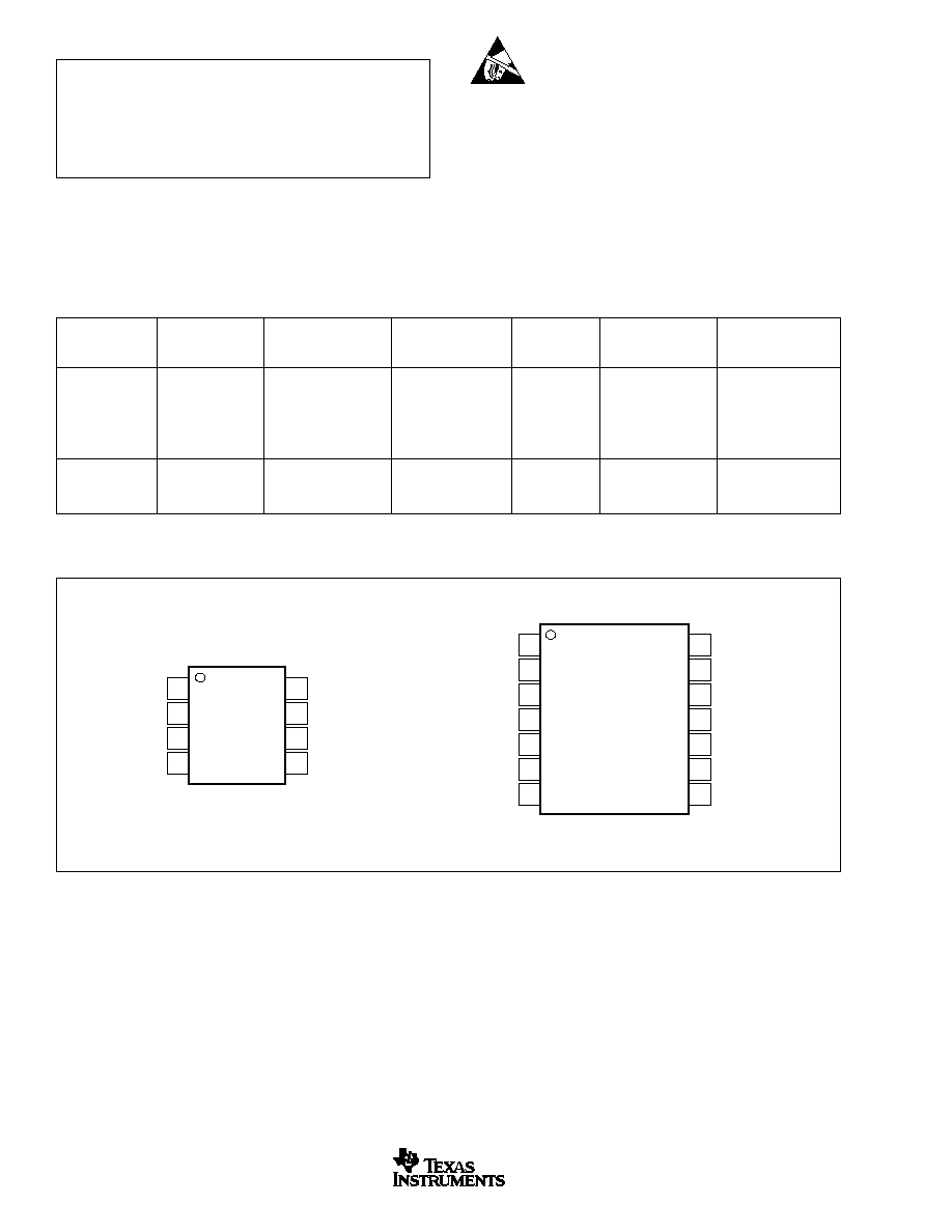
PIN CONFIGURATION
Top View
RG
V
IN
≠
V
IN
+
V≠
Shutdown
V+
V
OUT
REF
INA331
MSOP-8 (DGK)
1
2
3
4
8
7
6
5
1
2
3
4
5
6
7
14
13
12
11
10
9
8
Shutdown A
V
OUT
A
REFA
V+
REFB
V
OUT
B
Shutdown B
RGA
V
IN
≠A
V
IN
+A
V≠
V
IN
+B
V
IN
≠B
RGB
INA2331
Dual, TSSOP-14 (PW)
NOTE: (1) For the most current specifications and package information, refer to our web site at www.ti.com.
INA331, INA2331
SBOS215B
3
www.ti.com
ELECTRICAL CHARACTERISTICS: V
S
= +2.7V to +5.5V
Boldface limits apply over the specified temperature range, T
A
= ≠55
∞
C to 125
∞
C.
At T
A
= +25
∞
C, R
L
= 10k
, G = 25, and V
REF
= V
S
/2, unless otherwise noted.
INA331AIDGK
INA331IDGK
INA2331AIPW
PARAMETER
CONDITION
MIN
TYP
MAX
MIN
TYP
MAX
UNITS
INPUT
Input Offset Voltage, RTI
V
S
= +5V
±
250
±
500
±
1000
µ
V
Over Temperature
V
OS
±
1.7
±
2.1
mV
Temperature Coefficient
dV
OS
/dT
±
5
µ
V/
∞
C
vs Power Supply
PSRR
V
S
= +2.7V to +5.5V
±
50
±
200
µ
V/V
vs Temperature
±
220
µ
V/V
Long-Term Stability
±
0.4
µ
V/month
Input Impedance
10
13
|| 3
|| pF
Input Common-Mode Range
V
S
= 2.7V
0.35
1.5
V
V
S
= 5V
0.55
3.8
V
Common-Mode Rejection
CMRR
V
S
= 5V, V
CM
= 0.55V to 3.8V
90
94
80
dB
≠40
∞
C to +85
∞
C
V
S
= 5V, V
CM
= 0.55V to 3.8V
77
75
dB
Over Temperature
V
S
= 5V, V
CM
= 0.55V to 3.8V
72
70
dB
V
S
= 2.7V, V
CM
= 0.35V to 1.5V
94
dB
Crosstalk, Dual
114
dB
INPUT BIAS CURRENT
V
CM
= V
S
/2
Bias Current
I
B
±
0.5
±
10
pA
Offset Current
I
OS
±
0.5
±
10
pA
NOISE, RTI
R
S
= 0
Voltage Noise: f = 10Hz
e
N
280
nV/
Hz
f = 100Hz
96
nV/
Hz
f = 1kHz
46
nV/
Hz
f = 0.1Hz to 10Hz
7
µ
Vp-p
Current Noise: f = 1kHz
i
N
0.5
fA/
Hz
GAIN
(1)
Gain Equation, Externally Set
G > 5
G = 5 + (5R
2
/R
1
)
Range of Gain
5
1000
V/V
Gain Error
G = 5
±
0.02
±
0.1
%
vs Temperature
G = 5
±
2
±
10
ppm/
∞
C
Nonlinearity
G = 25
(2)
, V
S
= 5V, V
O
= 0.05 to 4.95
±
0.001
±
0.010
% of FS
Over Temperature
±
0.002
±
0.015
% of FS
OUTPUT
Output Voltage Swing from Rail
(3)
R
L
= 10k
50
25
mV
Over Temperature
G > 10
50
mV
Capacitance Load Drive
See Typical Characteristics
pF
Short-Circuit Current
+48/≠32
mA
FREQUENCY RESPONSE
Bandwidth, ≠3dB
BW
G = 25
2.0
MHz
Slew Rate
SR
V
S
= 5V, G = 25
5
V/
µ
s
Settling Time, 0.1%
t
S
G = 25, C
L
= 100pF, V
O
= 2V step
1.7
µ
s
0.01%
2.5
µ
s
Overload Recovery
50% Input Overload G = 25
2
µ
s
POWER SUPPLY
Specified Voltage Range
+2.7
+5.5
V
Operating Voltage Range
+2.5 to +5.5
V
Quiescent Current per Channel
I
Q
V
SD
> 2.5
(3)
415
490
µ
A
Over Temperature
600
µ
A
Shutdown Quiescent Current/Chan
I
SD
V
SD
< 0.8
(3)
0.01
1
µ
A
TEMPERATURE RANGE
Specified Range
≠55
+125
∞
C
Operating/Storage Range
≠65
+150
∞
C
Thermal Resistance
JA
MSOP-8, TSSOP-14 Surface Mount
150
∞
C/W
Specifications same as INA331IDGK
NOTES: (1) Does not include errors from external gain setting resistors. (2) Output voltage swings are measured between the output and power-supply rails. Output
swings to rail only if G
10. Output does not swing to positive rail if gain is less than 10. (3) See typical characteristic "Percent Overshoot vs Load Capacitance."
(4) See typical characteristic "Shutdown Voltage vs Supply Voltage."
INA331, INA2331
SBOS215B
4
www.ti.com
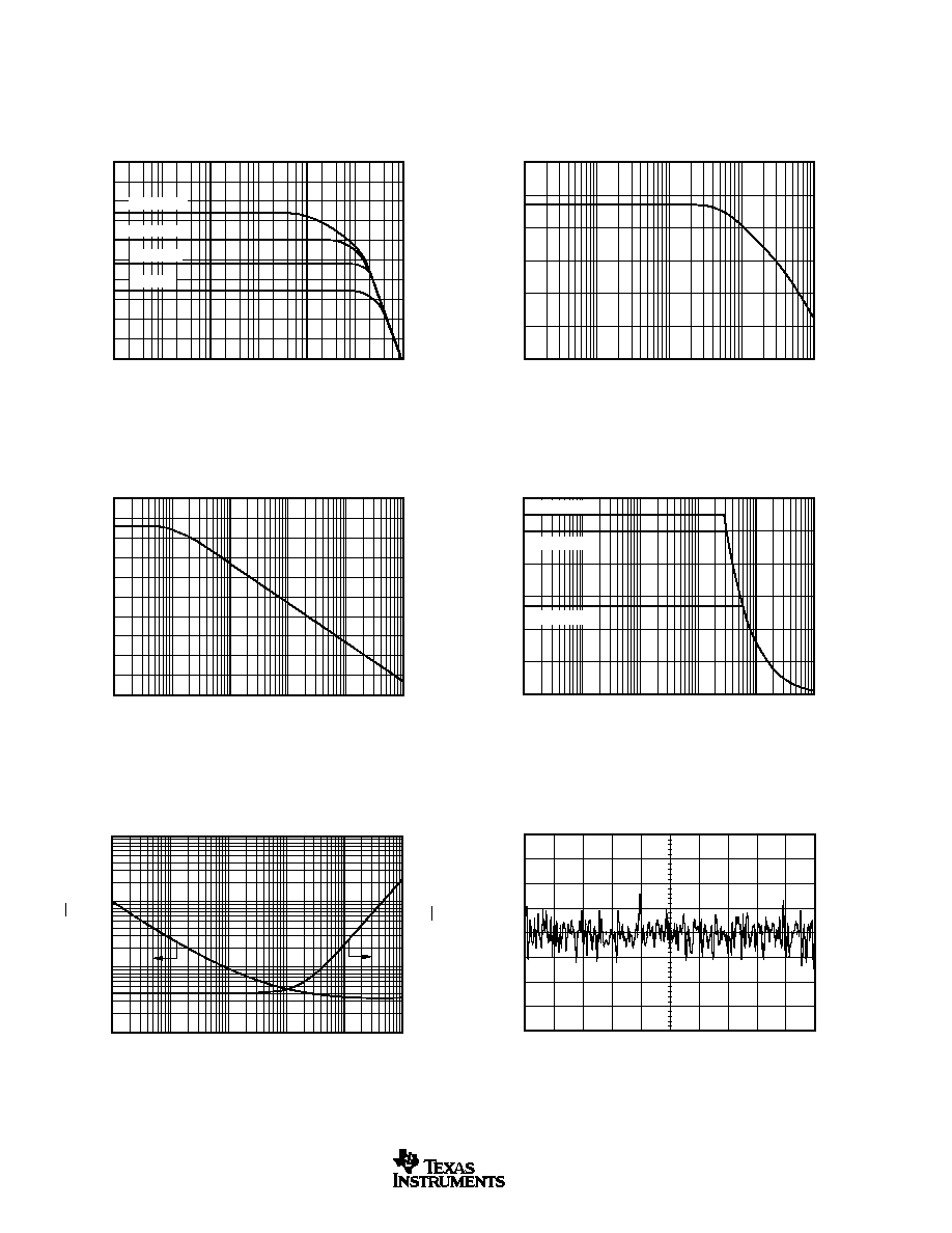
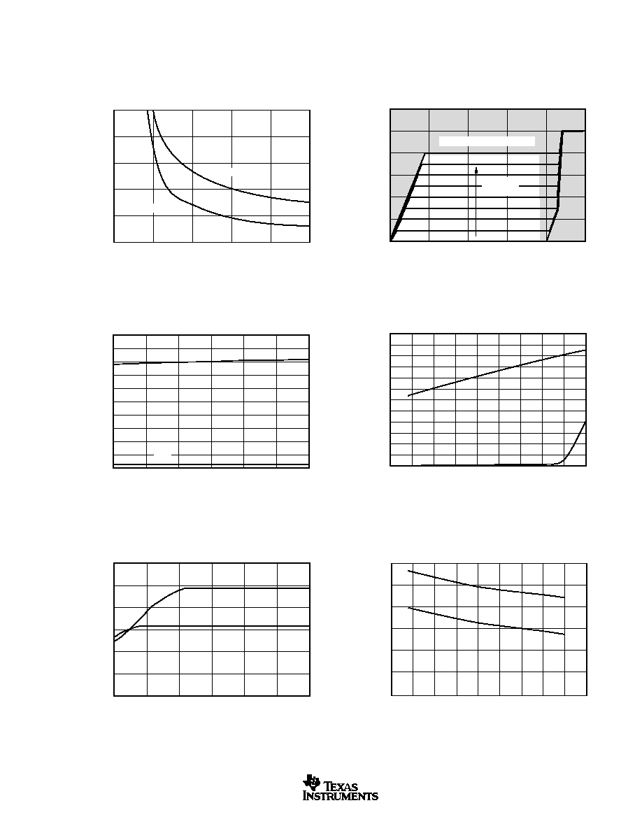
TYPICAL CHARACTERISTICS
At T
A
= +25
∞
C, V
S
= 5V, V
CM
= V
S
/2, R
L
= 10k
, and C
L
= 100pF, unless otherwise noted.
GAIN vs FREQUENCY
10
Gain (dB)
Frequency (Hz)
100
1k
10k
100k
1M
10M
80
70
60
50
40
30
20
10
0
≠10
≠20
Gain = 500
Gain = 100
Gain = 25
Gain = 5
COMMON-MODE REJECTION RATIO
vs FREQUENCY
10
CMRR (dB)
Frequency (Hz)
100
1k
10k
100k
120
100
80
60
40
20
0
POWER-SUPPLY REJECTION RATIO
vs FREQUENCY
1
PSRR (dB)
Frequency (Hz)
10
100
1k
10k
100k
100
90
80
70
60
50
40
30
20
10
0
MAXIMUM OUTPUT VOLTAGE vs FREQUENCY
100
Maximum Output Voltage (Vp-p)
Frequency (Hz)
1k
10k
100k
1M
10M
6
5
4
3
2
1
0
V
S
= 5.5V
V
S
= 5.0V
V
S
= 2.7V
NOISE vs FREQUENCY
1
V
NOISE
(nV/
Hz)
I
NOISE
(fA/
Hz)
Frequency (Hz)
10
100
1k
10k
100k
10k
1k
100
10
100
10
1
0.1
0.1Hz TO 10Hz VOLTAGE NOISE
1s/div
2
µ
V/div
INA331, INA2331
SBOS215B
5
www.ti.com
TYPICAL CHARACTERISTICS
(Cont.)
At T
A
= +25
∞
C, V
S
= 5V, V
CM
= V
S
/2, R
L
= 10k
, and C
L
= 100pF, unless otherwise noted.
COMMON-MODE INPUT RANGE
vs REFERENCE VOLTAGE
0
Output
--
Referred to Ground (V)
Input Common-Mode Voltage (V)
1
2
3
4
5
6
5
4
3
2
1
0
Outside of Normal Operation
REF
Increasing
QUIESCENT CURRENT AND SHUTDOWN CURRENT
vs POWER SUPPLY
I
Q
(
µ
A), I
SD
(nA)
Supply Voltage (V)
2.5
3
3.5
4
4.5
5
5.5
500
450
400
350
300
250
200
150
100
50
0
I
Q
I
SD
SHORT-CIRCUIT CURRENT vs POWER SUPPLY
I
SC
(mA)
Supply Voltage (V)
2.5
3
3.5
4
4.5
5
5.5
60
50
40
30
20
10
0
I
SC+
I
SC≠
SHORT-CIRCUIT CURRENT vs TEMPERATURE
I
SC
(mA)
Temperature (
∞
C)
≠75
25
≠50
≠25
0
50
75
100
125
150
60
50
40
30
20
10
0
I
SC+
I
SC≠
OUTPUT SWING vs LOAD RESISTANCE
Swing to Rail (mV)
R
LOAD
(
)
0
10k
20k
30k
40k
50k
25
20
15
10
5
0
To Positive Rail
To Negative Rail
QUIESCENT CURRENT AND SHUTDOWN CURRENT
vs TEMPERATURE
I
Q
(
µ
A)
Temperature (
∞
C)
≠75
≠50
≠25
0
25
50
75
100
125
150
600
550
500
450
400
350
300
250
200
150
100
50
0
I
Q
I
SD