Document Outline
- FEATURES
- APPLICATIONS
- DESCRIPTION
- ABSOLUTE MAXIMUM RATINGS
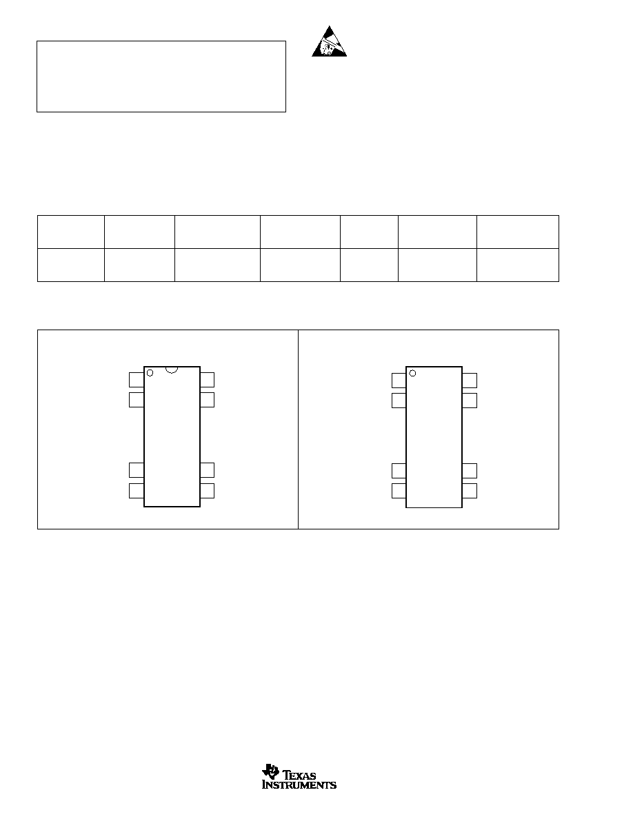
- PACKAGE/ORDERING INFORMATION
- PIN CONFIGURATIONS
- ELECTRICAL CHARACTERISTICS
- TYPICAL CHARACTERISTICS
- THEORY OF OPERATION
- BASIC OPERATION
- SIGNAL AND SUPPLY CONNECTIONS
- CARRIER FREQUENCY CONSIDERATIONS
- ISOLATION MODE VOLTAGE INDUCED ERRORS
- HIGH IMV dV/dt ERRORS
- HIGH VOLTAGE TESTING
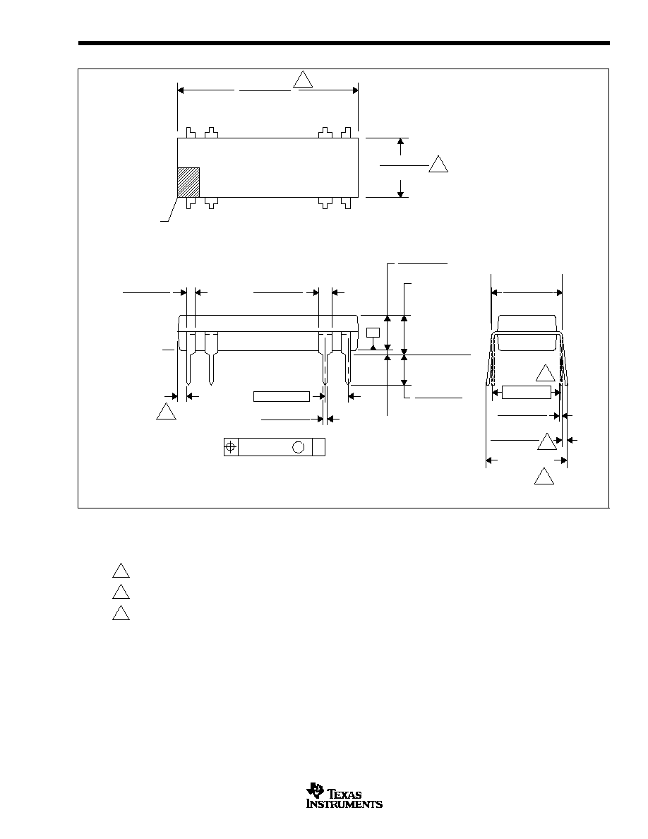
- PACKAGE DRAWINGS
- NVF (R-PDIP-T8/16) PLASTIC DUAL-IN-LINE
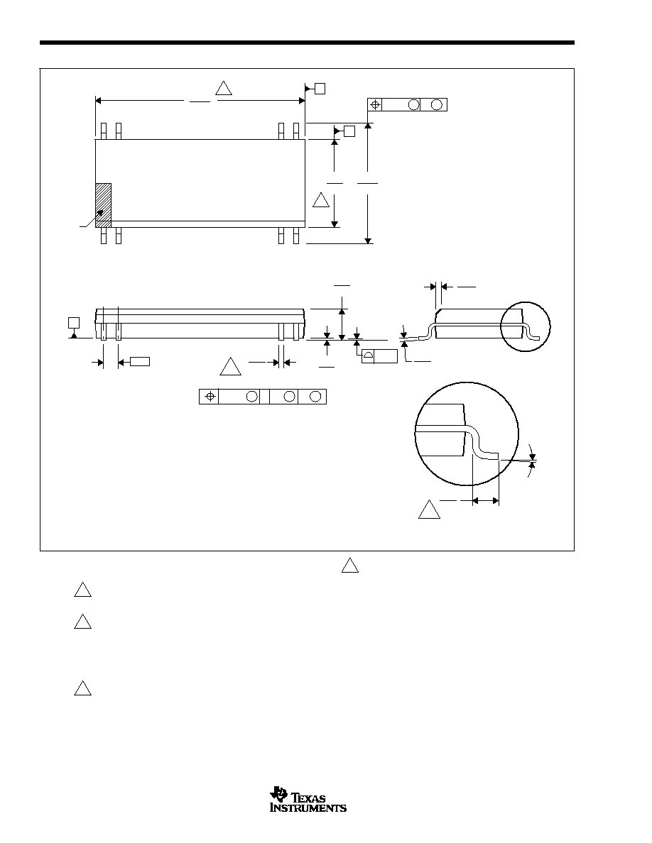
- DVA (R-PDSO-G8/28) PLASTIC SMALL-OUTLINE
FEATURES
q
100% TESTED FOR HIGH-VOLTAGE
BREAKDOWN
q
RATED 1500Vrms
q
HIGH IMR: 140dB at 60Hz
q
0.010% max NONLINEARITY
q
BIPOLAR OPERATION: V
O
=
±
10V
q
DIP-16 AND SO-28
q
EASE OF USE: Fixed Unity Gain Configuration
q
±
4.5V to
±
18V SUPPLY RANGE
APPLICATIONS
q
INDUSTRIAL PROCESS CONTROL:
Transducer Isolator, Isolator for Thermo-
couples, RTDs, Pressure Bridges, and
Flow Meters, 4-20mA Loop Isolation
q
GROUND LOOP ELIMINATION
q
MOTOR AND SCR CONTROL
q
POWER MONITORING
q
PC-BASED DATA ACQUISITION
q
TEST EQUIPMENT
DESCRIPTION
The ISO124 is a precision isolation amplifier incorporating a
novel duty cycle modulation-demodulation technique. The
signal is transmitted digitally across a 2pF differential capaci-
tive barrier. With digital modulation, the barrier characteris-
tics do not affect signal integrity, resulting in excellent reliabil-
ity and good high-frequency transient immunity across the
barrier. Both barrier capacitors are imbedded in the plastic
body of the package.
The ISO124 is easy to use. No external components are
required for operation. The key specifications are 0.010%
max nonlinearity, 50kHz signal bandwidth, and 200
µ
V/
∞
C
V
OS
drift. A power supply range of
±
4.5V to
±
18V and
quiescent currents of
±
5.0mA on V
S1
and
±
5.5mA on V
S2
make these amplifiers ideal for a wide range of applications.
The ISO124 is available in DIP-16 and SO-28 plastic surface
mount packages.
Precision Lowest-Cost
ISOLATION AMPLIFIER
+V
S1
V
IN
V
OUT
≠V
S1
+V
S2
Gnd 2
≠V
S2
Gnd 1
ISO1
24
ISO124
ISO124
SBOS074B ≠ SEPTEMBER 1997 ≠ REVISED APRIL 2003
www.ti.com
PRODUCTION DATA information is current as of publication date.
Products conform to specifications per the terms of Texas Instruments
standard warranty. Production processing does not necessarily include
testing of all parameters.
Copyright © 1997-2003, Texas Instruments Incorporated
Please be aware that an important notice concerning availability, standard warranty, and use in critical applications of
Texas Instruments semiconductor products and disclaimers thereto appears at the end of this data sheet.
ISO124
2
SBOS074B
www.ti.com
SPECIFIED
PACKAGE
TEMPERATURE
PACKAGE
ORDERING
TRANSPORT
PRODUCT
PACKAGE-LEAD
DESIGNATOR
(1)
RANGE
MARKING
NUMBER
MEDIA, QUANTITY
ISO124P
Plastic DIP-16
NVF
≠25
∞
C to +85
∞
C
ISO124P
ISO124P
Rails, 50
ISO124U
Plastic SO-28
DVA
≠25
∞
C to +85
∞
C
ISO124U
ISO124U
Rails, 28
"
"
"
"
ISO124U
ISO124U/1K
Tape and Reel, 1000
Supply Voltage ...................................................................................
±
18V
V
IN
......................................................................................................
±
100V
Continuous Isolation Voltage ..................................................... 1500Vrms
Junction Temperature .................................................................... +150
∞
C
Storage Temperature ..................................................................... +125
∞
C
Lead Temperature (soldering, 10s) ............................................... +300
∞
C
Output Short to Common ......................................................... Continuous
NOTE: (1) Stresses above these ratings may cause permanent damage.
Exposure to absolute maximum conditions for extended periods may degrade
device reliability.
Top View
DIP
Top View
SO
PIN CONFIGURATIONS
ABSOLUTE MAXIMUM RATINGS
(1)
ELECTROSTATIC
DISCHARGE SENSITIVITY
This integrated circuit can be damaged by ESD. Texas Instru-
ments recommends that all integrated circuits be handled with
appropriate precautions. Failure to observe proper handling
and installation procedures can cause damage.
ESD damage can range from subtle performance degradation
to complete device failure. Precision integrated circuits may be
more susceptible to damage because very small parametric
changes could cause the device not to meet its published
specifications.
PACKAGE/ORDERING INFORMATION
NOTE: (1) For the most current specifications and package information, refer to our web site at www.ti.com.
1
2
16
15
10
9
7
8
+V
S1
≠V
S1
V
OUT
Gnd 2
Gnd 1
V
IN
≠V
S2
+V
S2
1
2
28
27
16
15
13
14
+V
S1
≠V
S1
V
OUT
Gnd 2
Gnd 1
V
IN
≠V
S2
+V
S2

ISO124
3
SBOS074B
www.ti.com
ELECTRICAL CHARACTERISTICS
At T
A
= +25
∞
C , V
S1
= V
S2
=
±
15V, and R
L
= 2k
, unless otherwise noted.
ISO124P, U
PARAMETER
CONDITIONS
MIN
TYP
MAX
UNITS
ISOLATION
Rated Voltage, continuous ac 60Hz
1500
Vac
100% Test
(1)
1s, 5pc PD
2400
Vac
Isolation Mode Rejection
60Hz
140
dB
Barrier Impedance
10
14
|| 2
|| pF
Leakage Current at 60Hz
V
ISO
= 240Vrms
0.18
0.5
µ
Arms
GAIN
V
O
=
±
10V
Nominal Gain
1
V/V
Gain Error
±
0.05
±
0.50
%FSR
Gain vs Temperature
±
10
ppm/
∞
C
Nonlinearity
(2)
±
0.005
±
0.010
%FSR
INPUT OFFSET VOLTAGE
Initial Offset
±
20
±
50
mV
vs Temperature
±
200
µ
V/
∞
C
vs Supply
±
2
mV/V
Noise
4
µ
V/
Hz
INPUT
Voltage Range
±
10
±
12.5
V
Resistance
200
k
OUTPUT
Voltage Range
±
10
±
12.5
V
Current Drive
±
5
±
15
mA
Capacitive Load Drive
0.1
µ
F
Ripple Voltage
(3)
20
mVp-p
FREQUENCY RESPONSE
Small-Signal Bandwidth
50
kHz
Slew Rate
2
V/
µ
s
Settling Time
V
O
=
±
10V
0.1%
50
µ
s
0.01%
350
µ
s
Overload Recovery Time
150
µ
s
POWER SUPPLIES
Rated Voltage
±
15
V
Voltage Range
±
4.5
±
18
V
Quiescent Current: V
S1
±
5.0
±
7.0
mA
V
S2
±
5.5
±
7.0
mA
TEMPERATURE RANGE
Specification
≠25
+85
∞
C
Operating
≠25
+85
∞
C
Storage
≠40
+125
∞
C
Thermal Resistance,
JA
100
∞
C/W
JC
65
∞
C/W
NOTES: (1) Tested at 1.6 X rated, fail on 5pC partial discharge. (2) Nonlinearity is the peak deviation of the output voltage from the best-fit straight line. It is expressed
as the ratio of deviation to FSR. (3) Ripple frequency is at carrier frequency (500kHz).
ISO124
4
SBOS074B
www.ti.com
Time (
µ
s)
Time (
µ
s)
+10
0
≠10
0
STEP RESPONSE
500
1000
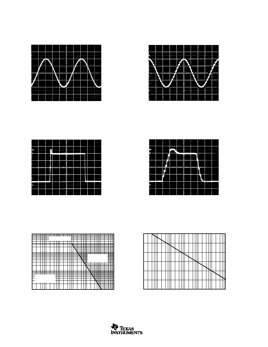
TYPICAL CHARACTERISTICS
At T
A
= +25
∞
C, and V
S
=
±
15V, unless otherwise noted.
+10
0
≠10
0
SINE RESPONSE
(f = 2kHz)
Output Voltage (V)
Output Voltage (V)
SINE RESPONSE
(f = 20kHz)
Time (
µ
s)
+10
0
≠10
0
100
50
Output Voltage (V)
Time (
µ
s)
+10
0
≠10
0
STEP RESPONSE
100
50
Output Voltage (V)
1000
500
ISOLATION VOLTAGE
vs FREQUENCY
Frequency (Hz)
Peak Isolation Voltage
100
1k
10k
100k
1M
10M
100M
1k
100
0
2.1k
Degraded
Performance
Typical
Performance
Max DC Rating
IMR vs FREQUENCY
Frequency (Hz)
IMR (dB)
160
140
120
100
80
60
40
1
10
100
1k
10k
100k
1M
ISO124
5
SBOS074B
www.ti.com
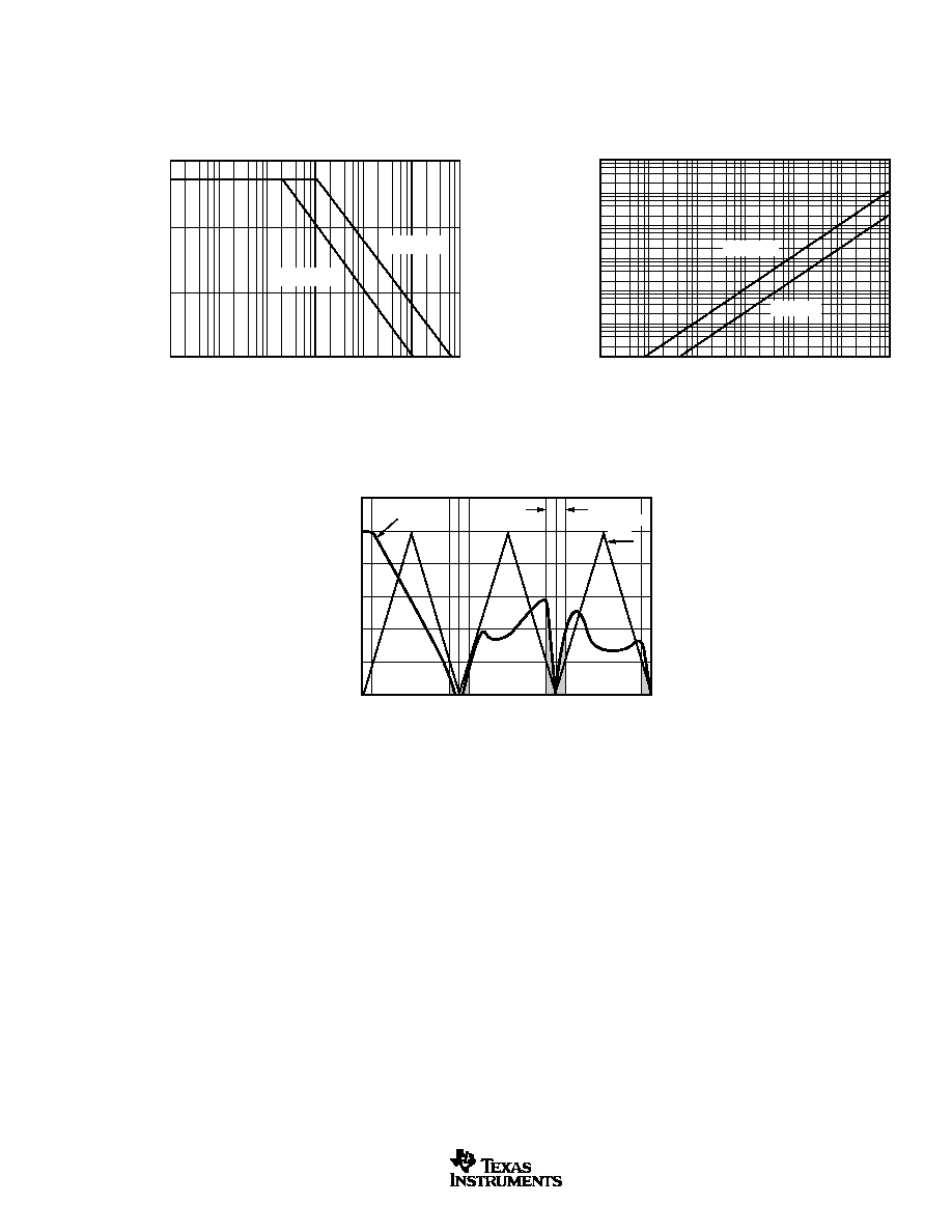
TYPICAL CHARACTERISTICS
(Cont.)
At T
A
= +25
∞
C, and V
S
=
±
15V, unless otherwise noted.
60
40
20
0
54
1
10
100
1k
10k
100k
1M
PSRR vs FREQUENCY
Frequency (Hz)
PSRR (dB)
≠V
S1
, ≠V
S2
+V
S1
, +V
S2
100mA
10mA
1mA
100
µ
A
10
µ
A
1
µ
A
0.1
µ
A
1
10
100
1k
10k
100k
1M
ISOLATION LEAKAGE CURRENT vs FREQUENCY
Frequency (Hz)
Leakage Current (rms)
1500Vrms
240Vrms
0
≠10
≠20
≠30
≠40
250
200
150
100
50
0
500k
1M
1.5M
SIGNAL RESPONSE TO
INPUTS GREATER THAN 250kHz
Input Frequency (Hz)
V
OUT
/V
IN
(dBm)
Frequency Out
(NOTE: Shaded area shows aliasing frequencies that
cannot be removed by a low-pass filter at the output.)
V
OUT
/V
IN
100kHz
Frequency
Out
ISO124
6
SBOS074B
www.ti.com
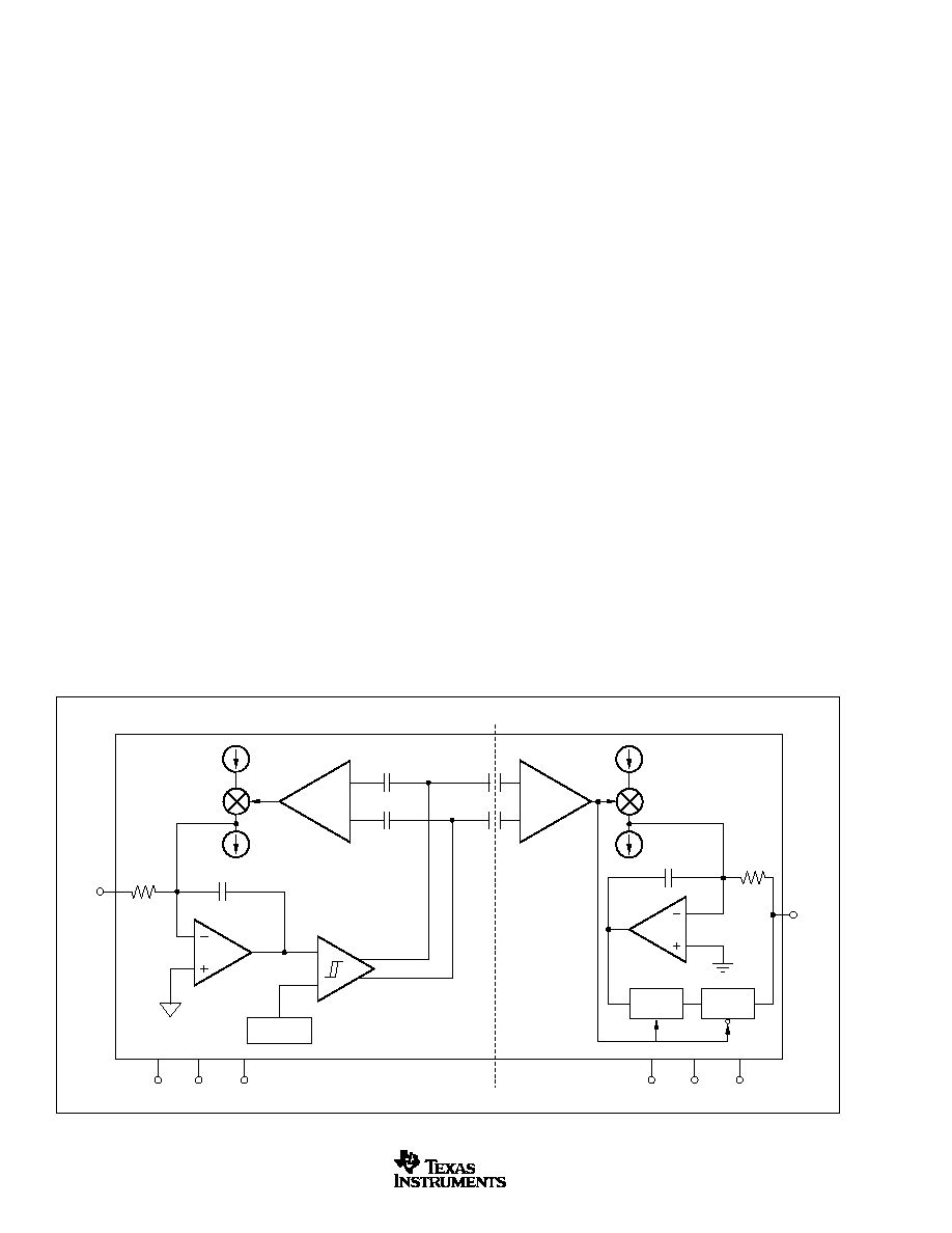
THEORY OF OPERATION
The ISO124 isolation amplifier uses an input and an output
section galvanically isolated by matched 1pF isolating ca-
pacitors built into the plastic package. The input is duty-cycle
modulated and transmitted digitally across the barrier. The
output section receives the modulated signal, converts it
back to an analog voltage and removes the ripple component
inherent in the demodulation. Input and output sections are
fabricated, then laser trimmed for exceptional circuitry match-
ing common to both input and output sections. The sections
are then mounted on opposite ends of the package with the
isolating capacitors mounted between the two sections. The
transistor count of the ISO124 is 250 transistors.
MODULATOR
An input amplifier (A1, as shown in Figure 1) integrates the
difference between the input current (V
IN
/200k
) and a
switched
±
100
µ
A current source. This current source is
implemented by a switchable 200
µ
A source and a fixed
100
µ
A current sink. To understand the basic operation of the
modulator, assume that V
IN
= 0.0V. The integrator will ramp
in one direction until the comparator threshold is exceeded.
The comparator and sense amp will force the current source
to switch; the resultant signal is a triangular waveform with a
50% duty cycle. The internal oscillator forces the current
source to switch at 500kHz. The resultant capacitor drive is
a complementary duty-cycle modulation square wave.
DEMODULATOR
The sense amplifier detects the signal transitions across the
capacitive barrier and drives a switched current source into
integrator A2. The output stage balances the duty-cycle
FIGURE 1. Block Diagram.
modulated current against the feedback current through the
200k
feedback resistor, resulting in an average value at the
V
OUT
pin equal to V
IN
. The sample-and-hold amplifiers in the
output feedback loop serve to remove undesired ripple volt-
ages inherent in the demodulation process.
BASIC OPERATION
SIGNAL AND SUPPLY CONNECTIONS
Each power-supply pin should be bypassed with 1
µ
F tantalum
capacitors located as close to the amplifier as possible. The
internal frequency of the modulator/demodulator is set at
500kHz by an internal oscillator. Therefore, if it is desired to
minimize any feedthrough noise (beat frequencies) from a
DC/DC converter, use a
filter on the supplies (see Figure 4).
The ISO124 output has a 500kHz ripple of 20mV, which can
be removed with a simple 2-pole low-pass filter with a 100kHz
cutoff using a low-cost op amp (see Figure 4).
The input to the modulator is a current (set by the 200k
integrator input resistor) that makes it possible to have an
input voltage greater than the input supplies, as long as the
output supply is at least
±
15V. It is therefore possible, when
using an unregulated DC/DC converter, to minimize PSR
related output errors with
±
5V voltage regulators on the
isolated side and still get the full
±
10V input and output swing.
See Figure 9 for an example of this application.
CARRIER FREQUENCY CONSIDERATIONS
The ISO124 amplifier transmits the signal across the isola-
tion barrier by a 500kHz duty-cycle modulation technique.
For input signals having frequencies below 250kHz, this
system works like any linear amplifier. But for frequencies
200k
1pF
1pF
1pF
1pF
150pF
Osc
200
µ
A
100
µ
A
Sense
200
µ
A
100
µ
A
200k
150pF
S/H
G = 1
S/H
G = 6
Sense
A2
A1
+V
S2
Gnd 2
≠V
S2
+V
S1
Gnd 1
≠V
S1
V
IN
V
OUT
Isolation Barrier
ISO124
7
SBOS074B
www.ti.com
1
2
7
9
10
8
PGA102
ISO124
ISO150
1
2
3
16
4
6
7
8
5
15
15
+15V ≠15V
+15V ≠15V
V
IN
V
OUT
A
0
A
1
above 250kHz, the behavior is similar to that of a sampling
amplifier. The typical characteristic "Signal Response to
Inputs Greater Than 250kHz" shows this behavior graphi-
cally; at input frequencies above 250kHz, the device gener-
ates an output signal component of reduced magnitude at a
frequency below 250kHz. This is the aliasing effect of sam-
pling at frequencies less than 2 times the signal frequency
(the Nyquist frequency). Note that at the carrier frequency
and its harmonics, both the frequency and amplitude of the
aliasing go to zero.
ISOLATION MODE VOLTAGE INDUCED ERRORS
IMV can induce errors at the output as indicated by the plots of IMV
vs Frequency. It should be noted that if the IMV frequency exceeds
250kHz, the output also will display spurious outputs (aliasing) in
a manner similar to that for V
IN
> 250kHz and the amplifier
response will be identical to that shown in the "Signal Response to
Inputs Greater Than 250kHz" typical characteristic. This occurs
because IMV-induced errors behave like input-referred error sig-
nals. To predict the total error, divide the isolation voltage by the
IMR shown in the "IMR versus Frequency" typical performance
curve and compute the amplifier response to this input-referred
error signal from the data given in the "Signal Response to Inputs
Greater Than 250kHz" typical characteristic. For example, if a
800kHz 1000Vrms IMR is present, then a total of
[(≠60dB) + (≠30dB)] x (1000V) = 32mV error signal at 200kHz plus
a 1V, 800kHz error signal will be present at the output.
HIGH IMV dV/dt ERRORS
As the IMV frequency increases and the dV/dt exceeds
1000V/
µ
s, the sense amp may start to false trigger, and the
output will display spurious errors. The common-mode cur-
rent being sent across the barrier by the high slew rate is the
cause of the false triggering of the sense amplifier. Lowering
the power-supply voltages below
±
15V may decrease the
dV/dt to 500V/
µ
s for typical performance.
HIGH VOLTAGE TESTING
Texas Instruments has adopted a partial discharge test
criterion that conforms to the German VDE0884 Optocoupler
Standards. This method requires the measurement of minute
current pulses (< 5pC) while applying 2400Vrms, 60Hz high-
voltage stress across every ISO124 isolation barrier. No
partial discharge may be initiated to pass this test. This
criterion confirms transient overvoltage (1.6 x 1500Vrms)
protection without damage to the ISO124. Lifetest results
verify the absence of failure under continuous rated voltage
and maximum temperature.
This new test method represents the "state-of-the art" for
non-destructive high-voltage reliability testing. It is based on
the effects of non-uniform fields that exist in heterogeneous
dielectric material during barrier degradation. In the case of
void non-uniformities, electric field stress begins to ionize the
void region before bridging the entire high-voltage barrier.
The transient conduction of charge during and after the
ionization can be detected externally as a burst of 0.01-0.1
µ
s
current pulses that repeat on each ac voltage cycle. The
minimum ac barrier voltage that initiates partial discharge is
defined as the "inception voltage." Decreasing the barrier
voltage to a lower level is required before partial discharge
ceases and is defined as the "extinction voltage." We have
characterized and developed the package insulation pro-
cesses to yield an inception voltage in excess of 2400Vrms
so that transient overvoltages below this level will not dam-
age the ISO124. The extinction voltage is above 1500Vrms
so that even overvoltage induced partial discharge will cease
once the barrier voltage is reduced to the 1500Vrms (rated)
level. Older high-voltage test methods relied on applying a
large enough overvoltage (above rating) to break down
marginal parts, but not so high as to damage good ones. Our
new partial discharge testing gives us more confidence in
barrier reliability than breakdown/no breakdown criteria.
FIGURE 3. Programmable-Gain Isolation Channel with Gains
of 1, 10, and 100.
FIGURE 2. Basic Signal and Power Connections.
+V
S1
+V
S2
Gnd
Gnd
V
IN
V
OUT
≠V
S1
±
V
S1
±
V
S2
≠V
S2
1
µ
F
1
µ
F 1
µ
F
1
µ
F
Isolation Barrier
ISO124
ISO124
8
SBOS074B
www.ti.com
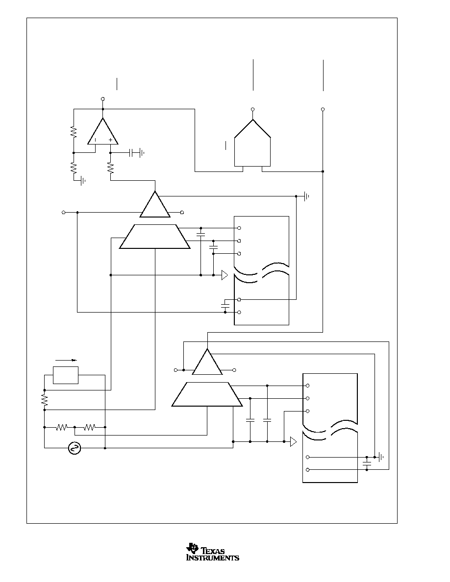
FIGURE 5. Battery Monitor for a 600V Battery Power System. (Derives input power from the battery.)
FIGURE 4. Optional
Filter to Minimize Power-Supply Feedthrough Noise; Output Filter to Remove 500kHz Carrier Ripple. For
more information concerning output filters refer to Application Notes SBPA012 and SBFA001.
V
IN
V
OUT
= V
IN
Isolation Barrier
ISO124
+V
S2
+V
S1
≠V
S1
±
V
S1
≠V
S2
Gnd2
Gnd1
R
1
4.75k
R
2
9.76k
1
µ
F
1
µ
F
1
µ
F
1
µ
F
10
µ
H
10
µ
H
±
V
S2
10
µ
H
10
µ
H
1
µ
F
1
µ
F
1
µ
F 1
µ
F
C
1
220pF
C
2
1000pF
OPA237
15
1
9
10
7
2
e
50
= 12V
8
≠V
16
+V
15
1
9
10
7
2
10k
8
≠V
16
+V
10k
e
49
= 12V
e
2
= 12V
e
1
= 12V
10k
10k
Charge/Discharge Control
INA105
25k
25k
25k
25k
2
3
1
e
50
V =
2
+V ≠V
7
4
5
6
e
1
V =
2
Multiplexer
Control
Section
ISO124
This Section Repeated 49 Times.
ISO124

ISO124
9
SBOS074B
www.ti.com
FIGURE 6. Thermocouple Amplifier with Ground Loop Elimination, Cold Junction Compensation, and Up-scale Burn-out.
FIGURE 7. Isolated 4-20mA Instrument Loop. (RTD shown.)
R
CM
1k
RCV420
XTR105
R
G
R
Z
(1)
13
3
4
2
6
7
10
14
1
0.01
µ
F
4-20mA
RTD
(PT100)
0.8mA
0.8mA
1.6mA
14
15
16
3
2
10
4
12
11
5, 13
15
16
2
1
Gnd
≠V
S
= ≠15V
on PWS740
+V
S
= 15V on PWS740
9
10
7
8
≠V
+V
ISO124
V
OUT
0V - 5V
NOTE: (1) R
Z
= RTD resistance at minimum measured temperature.
2
6
10.0V
4
REF102
INA114
or
INA128
+In
7
4
3
8
1
2
5
16
15
8
10
ISO124
7
V
OUT
9
6
≠In
+15V
+15V
≠15V
+15V ≠15V
ISA
TYPE
E
J
K
T
MATERIAL
Chromel
Constantan
Iron
Constantan
Chromel
Alumel
Copper
Constantan
SEEBACK
COEFFICIENT
(
µ
V/
∞
C)
58.5
50.2
39.4
38.0
R
2
(R
3
= 100
)
3.48k
4.12k
5.23k
5.49k
R
4
(R
5
+ R
6
= 100
)
56.2k
64.9k
80.6k
84.5k
+15V ≠15V
R
3
100
Ground Loop Through Conduit
NOTE: (1) ≠2.1mV/
∞
C at 2.00
µ
A.
R
1
27k
Isothermal
Block with
1N4148
(1)
R
2
1M
R
5
50
R
G
R
4
R
6
100
Zero Adj
Thermocouple
2
1
ISO124
10
SBOS074B
www.ti.com
FIGURE 8. Isolated Power Line Monitor.
15
V
≠
V+
10
7
9
8
ISO124
1
2
16
15
16
V
≠
V+
10
7
9
8
ISO124
1
2
0.47
µ
F
0.47
µ
F
0.47
µ
F
0.47
µ
F
0.47
µ
F
0.47
µ
F
R
S
R
D1
I
L
Load
R
D2
V
L
Y
X
XY
10
P
L
=
V
2
(R
D1
+ R
D2
)
R
S
R
D2
(V
2
)
MPY634
I
L
=
V
1
10R
S
(V
1
)
10k
2k
2k
0.01
µ
F
V
L
=
V
3
(R
D1
+ R
D2
)
R
D2
(V
3
)
OPA237
6
2
3
12
Isolated Power
5
6
7
12
Isolated Power
5
6
7

ISO124
11
SBOS074B
www.ti.com
FIGURE 10. Single-Supply Operation of the ISO124 Isolation Amplifier. For additional information refer to Application Note
SBOA004.
FIGURE 9. Improved PSR Using External Regulator.
NOTE: The input supplies can be subregulated to
±
5V to reduce
PSR related errors without reducing the
±
10V input range.
10
7
9
8
2
V
OUT
+15V
≠15V
V
IN
, up to
±
10V Swing
+5V
Regulator
MC78L05
≠5V
Regulator
MC79L05
0.47
µ
F 0.47
µ
F
0.1
µ
F
1
2
3
0.1
µ
F
0.47
µ
F
ISO124
3
1
2
16
1
Isolated Power
7
6
5
2
1
R
1
R
2
R
4
INA105
Difference Amp
R
3
R
S
2
3
4
IN4689
5.1V
Reference
5
7
6
1
V
IN
Signal Source
+
NOTE: (1) Select to match R .
NOTE: Since the amplifier is unity gain, the input
range is also the output range. The output can go
to ≠2V since the output section of the ISO amp
operates from dual supplies.
S
10k
15
≠V
S2
(≠15V)
+V
S2
(+15V)
V
S1
(+15V)
16
≠V
S1
Com 2
10
In
Gnd
R
C
(1)
V
S
(V)
20+
15
12
INPUT RANGE
(V)
(1)
≠2 to +10
≠2 to +5
≠2 to +2
7
9
8
ISO124
2
1
V
OUT
= V
IN

ISO124
12
SBOS074B
www.ti.com
FIGURE 12. Powered ISO Amp with Three-Port Isolation.
FIGURE 11. Input-Side Powered ISO Amp.
16
Gnd
V
IN
V≠
V+
V+
V≠
V
O
Gnd
15
1
2
1
2
10
9
7
8
Isolated Power
Input
Section
Output
Section
5
6
7
V
IN
Input
Gnd
+15V
≠15V
≠15V, 20mA
+15V, 20mA
Auxiliary
Isolated
Power
Output
Output
Gnd
V
O
ISO124
0.47
µ
F
0.47
µ
F
0.47
µ
F
16
Gnd
V
IN
V≠
V+
V+
V≠
V
O
Gnd
15
1
2
1
2
10
9
7
8
Isolated Power
Input
Section
Output
Section
5
6
7
+15V Gnd
Isolated Power
7
6
5
2
1
V
IN
Input
Gnd
+15V, 20mA
≠15V, 20mA
≠15V, 20mA
+15V, 20mA
Auxiliary
Isolated
Power
Output
Auxiliary
Isolated
Power
Output
Output
Gnd
V
O
ISO124
0.47
µ
F
0.47
µ
F
0.47
µ
F
0.47
µ
F
0.47
µ
F
ISO124
13
SBOS074B
www.ti.com
PACKAGE DRAWINGS
NVF (R-PDIP-T8/16)
PLASTIC DUAL-IN-LINE
4202501/A 08/01
0.150 (3,81)
0.115 (2,92)
C
0.005 (0,13)
MIN 4 PL
1
8
9
16
0.775 (21,34)
0.735 (18,67)
0.240 (6,10)
0.280 (7,11)
0.070 (1,78)
0.045 (1,14)
0.030 (0,76)
0.045 (1,14)
0.014 (0,36)
0.022 (0,56)
0.010 (0,25) M
C
0.210 (5,33)
0.195 (4,95)
0.115 (2,92)
0.300 (7,63)
MAX
0.430 (10,92)
0.000 (0,00)
0.060 (1,52)
0.014 (0,36)
0.008 (0,20)
0.325 (8,26)
0.300 (7,62)
Index
Area
0.015 (0,38)
MIN
0.100 (2,54)
Seating Plane
Base Plane
MAX
F
F
D
D
D
E
1/2 Lead
A. All linear dimensions are in inches (millimeters).
B. This drawing is subject to change without notice.
C. Falls within JEDEC MS-001-BB with the exception of lead
count.
D. Dimensions do not include mold flash or protrusions.
Mold flash or protrusions shall not exceed 0.010 (0,25).
E. Dimensions measured with the leads constrained to be
perpendicular to Datum C.
F. Dimensions are measured at the lead tips with the leads
unconstrained.
G. A visual index feature must be located within the
cross-hatched area.
ISO124
14
SBOS074B
www.ti.com
PACKAGE DRAWINGS (Cont.)
DVA (R-PDSO-G8/28)
PLASTIC SMALL-OUTLINE
4202103/B 08/01
Index
Area
1
1
4
15
28
Seating
Plane
17,70
18,10
7,60
7,40
10,01
10,65
2,35
2,65
0,30
0,10
0,51
0,33
0,32
0,23
0,25
0,75
x 45
∞
1,27
0,40
0
∞
≠8
∞
C
F
G
1,27
0,25 M
B
A
C
S
0,10
0,25
M
B
C
B
A
D
M
M
NOTES: A. All linear dimensions are in millimeters.
B. This drawing is subject to change without notice.
C. Body length dimension does not include mold
flash, protrusions, or gate burrs. Mold flash, protrusions,
and gate burrs shall not exceed 0,15 mm per side.
D. Body width dimension does not include inter-lead flash
or portrusions. Inter-lead flash and protrusions
shall not exceed 0,25 mm per side.
E. The chamfer on the body is optional. If it is not present,
a visual index feature must be located within the
cross-hatched area.
F. Lead dimension is the length of terminal for soldering
to a substrate.
G. Lead width, as measured 0,36 mm or greater
above the seating plane, shall not exceed a
maximum value of 0,61 mm.
H. Lead-to-lead coplanarity shall be less than
0,10 mm from seating plane.
I. Falls within JEDEC MS-013-AE with the exception
of the number of leads.

PACKAGING INFORMATION
ORDERABLE DEVICE
STATUS(1)
PACKAGE TYPE
PACKAGE DRAWING
PINS
PACKAGE QTY
ISO124P
ACTIVE
PDIP
NVF
8
50
ISO124U
ACTIVE
SOP
DVA
8
28
ISO124U/1K
ACTIVE
SOP
DVA
8
1000
(1) The marketing status values are defined as follows:
ACTIVE: Product device recommended for new designs.
LIFEBUY: TI has announced that the device will be discontinued, and a lifetime-buy period is in effect.
NRND: Not recommended for new designs. Device is in production to support existing customers, but TI does not recommend using this part in
a new design.
PREVIEW: Device has been announced but is not in production. Samples may or may not be available.
OBSOLETE: TI has discontinued the production of the device.
PACKAGE OPTION ADDENDUM
www.ti.com
3-Oct-2003

IMPORTANT NOTICE
Texas Instruments Incorporated and its subsidiaries (TI) reserve the right to make corrections, modifications,
enhancements, improvements, and other changes to its products and services at any time and to discontinue
any product or service without notice. Customers should obtain the latest relevant information before placing
orders and should verify that such information is current and complete. All products are sold subject to TI's terms
and conditions of sale supplied at the time of order acknowledgment.
TI warrants performance of its hardware products to the specifications applicable at the time of sale in
accordance with TI's standard warranty. Testing and other quality control techniques are used to the extent TI
deems necessary to support this warranty. Except where mandated by government requirements, testing of all
parameters of each product is not necessarily performed.
TI assumes no liability for applications assistance or customer product design. Customers are responsible for
their products and applications using TI components. To minimize the risks associated with customer products
and applications, customers should provide adequate design and operating safeguards.
TI does not warrant or represent that any license, either express or implied, is granted under any TI patent right,
copyright, mask work right, or other TI intellectual property right relating to any combination, machine, or process
in which TI products or services are used. Information published by TI regarding third-party products or services
does not constitute a license from TI to use such products or services or a warranty or endorsement thereof.
Use of such information may require a license from a third party under the patents or other intellectual property
of the third party, or a license from TI under the patents or other intellectual property of TI.
Reproduction of information in TI data books or data sheets is permissible only if reproduction is without
alteration and is accompanied by all associated warranties, conditions, limitations, and notices. Reproduction
of this information with alteration is an unfair and deceptive business practice. TI is not responsible or liable for
such altered documentation.
Resale of TI products or services with statements different from or beyond the parameters stated by TI for that
product or service voids all express and any implied warranties for the associated TI product or service and
is an unfair and deceptive business practice. TI is not responsible or liable for any such statements.
Following are URLs where you can obtain information on other Texas Instruments products and application
solutions:
Products
Applications
Amplifiers
amplifier.ti.com
Audio
www.ti.com/audio
Data Converters
dataconverter.ti.com
Automotive
www.ti.com/automotive
DSP
dsp.ti.com
Broadband
www.ti.com/broadband
Interface
interface.ti.com
Digital Control
www.ti.com/digitalcontrol
Logic
logic.ti.com
Military
www.ti.com/military
Power Mgmt
power.ti.com
Optical Networking
www.ti.com/opticalnetwork
Microcontrollers
microcontroller.ti.com
Security
www.ti.com/security
Telephony
www.ti.com/telephony
Video & Imaging
www.ti.com/video
Wireless
www.ti.com/wireless
Mailing Address:
Texas Instruments
Post Office Box 655303 Dallas, Texas 75265
Copyright
2003, Texas Instruments Incorporated