
LM193, LM293, LM293A, LM393
LM393A, LM2903, LM2903Q
DUAL DIFFERENTIAL COMPARATORS
SLCS005L ≠ JUNE 1976 ≠ REVISED AUGUST 2003
1
POST OFFICE BOX 655303
∑
DALLAS, TEXAS 75265
D
Single Supply or Dual Supplies
D
Wide Range of Supply Voltage
. . . 2 V to 36 V
D
Low Supply-Current Drain Independent of
Supply Voltage . . . 0.4 mA Typ Per
Comparator
D
Low Input Bias Current . . . 25 nA Typ
D
Low Input Offset Current . . . 3 nA Typ
(LM193)
D
Low Input Offset Voltage . . . 2 mV Typ
D
Common-Mode Input Voltage Range
Includes Ground
D
Differential Input Voltage Range Equal to
Maximum-Rated Supply Voltage . . .
±
36 V
D
Low Output Saturation Voltage
D
Output Compatible With TTL, MOS, and
CMOS
D
LM2903Q Available in Q-Temp Automotive
≠ High-Reliability Automotive Applications
≠ Configuration Control/Print Support
≠ Qualification to Automotive Standards
D
For Single Version in SOT23-5, See TL331
Data Sheet
description/ordering information
These devices consist of two independent voltage comparators that are designed to operate from a single power
supply over a wide range of voltages. Operation from dual supplies also is possible as long as the difference
between the two supplies is 2 V to 36 V, and V
CC
is at least 1.5 V more positive than the input common-mode
voltage. Current drain is independent of the supply voltage. The outputs can be connected to other
open-collector outputs to achieve wired-AND relationships.
The LM193 is characterized for operation from ≠55
∞
C to 125
∞
C. The LM293 and LM293A are characterized for
operation from ≠25
∞
C to 85
∞
C. The LM393 and LM393A are characterized for operation from 0
∞
C to 70
∞
C. The
LM2903 is characterized for operation from ≠40
∞
C to 125
∞
C. The LM2903Q is tested from ≠40
∞
C to 125
∞
C and
is manufactured to demanding automotive requirements.
Copyright
2003, Texas Instruments Incorporated
PRODUCTION DATA information is current as of publication date.
Products conform to specifications per the terms of Texas Instruments
standard warranty. Production processing does not necessarily include
testing of all parameters.
Please be aware that an important notice concerning availability, standard warranty, and use in critical applications of
Texas Instruments semiconductor products and disclaimers thereto appears at the end of this data sheet.
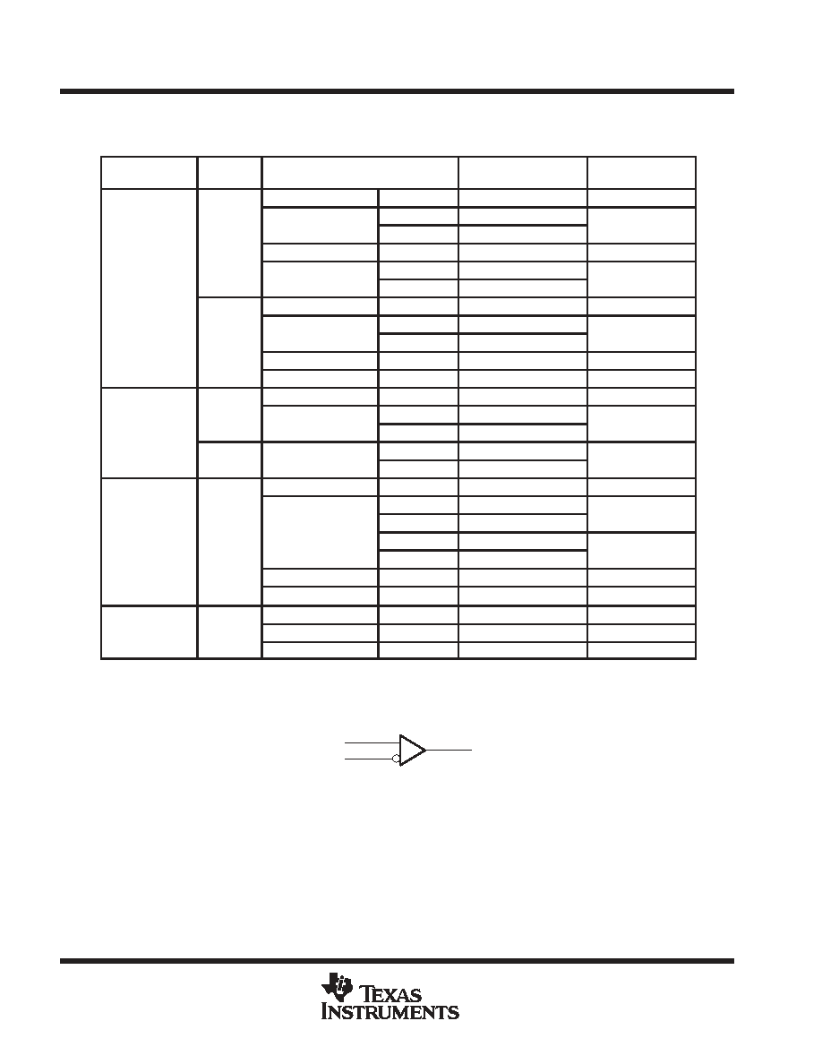
1
2
3
4
8
7
6
5
1OUT
1IN≠
1IN+
GND
V
CC
2OUT
2IN≠
2IN+
LM193 . . . D OR JG PACKAGE
LM293 . . . D OR P PACKAGE
LM293A . . . D PACKAGE
LM393, LM393A . . . D, P, PS, OR PW PACKAGE
LM2903 . . . D, P, PS, OR PW PACKAGE
LM2903Q . . . D PACKAGE
(TOP VIEW)
3
2
1 20 19
9 10 11 12 13
4
5
6
7
8
18
17
16
15
14
NC
2OUT
NC
2IN≠
NC
NC
1IN≠
NC
1IN+
NC
LM193 . . . FK PACKAGE
(TOP VIEW)
NC
1OUT
NC
2IN+
NC
V
NC
NC
GND
NC
CC
NC ≠ No internal connection
On products compliant to MIL-PRF-38535, all parameters are tested
unless otherwise noted. On all other products, production
processing does not necessarily include testing of all parameters.
LM193, LM293, LM293A, LM393
LM393A, LM2903, LM2903Q
DUAL DIFFERENTIAL COMPARATORS
SLCS005L ≠ JUNE 1976 ≠ REVISED AUGUST 2003
2
POST OFFICE BOX 655303
∑
DALLAS, TEXAS 75265
description/ordering information (continued)
ORDERING INFORMATION
TA
VIO(max)
AT 25
∞
C
PACKAGE
ORDERABLE
PART NUMBER
TOP-SIDE
MARKING
0 C to 70 C
5 mV
PDIP (P)
Tube of 50
LM393P
LM393P
0 C to 70 C
5 mV
SOIC (D)
Tube of 75
LM393D
LM393
0 C to 70 C
5 mV
SOIC (D)
Reel of 2500
LM393DR
LM393
0 C to 70 C
5 mV
SOP (PS)
Reel of 2000
LM393PSR
L393
0 C to 70 C
TSSOP (PW)
Tube of 150
LM393PW
L393
0
∞
C to 70
∞
C
TSSOP (PW)
Reel of 2000
LM393PWR
L393
2 mV
PDIP (P)
Tube of 50
LM393AP
LM393AP
2 mV
SOIC (D)
Tube of 75
LM393AD
LM393A
2 mV
SOIC (D)
Reel of 2500
LM393ADR
LM393A
SOP (PS)
Reel of 2000
LM393APSR
L393A
TSSOP (PW)
Reel of 2000
LM393APWR
L393A
≠25 C to 85 C
5 mV
PDIP (P)
Tube of 50
LM293P
LM293P
≠25 C to 85 C
5 mV
SOIC (D)
Tube of 75
LM293D
LM293
≠25
∞
C to 85
∞
C
SOIC (D)
Reel of 2500
LM293DR
LM293
2 mV
SOIC (D)
Tube of 75
LM293AD
LM293A
2 mV
SOIC (D)
Reel of 2500
LM293ADR
LM293A
≠40 C to 125 C
7 mV
PDIP (P)
Tube of 50
LM2903P
LM2903P
≠40 C to 125 C
7 mV
SOIC (D)
Tube of 75
LM2903D
LM2903
≠40 C to 125 C
7 mV
SOIC (D)
Reel of 2500
LM2903DR
LM2903
≠40
∞
C to 125
∞
C
7 mV
SOIC (D)
Tube of 75
LM2903QD
LM2903QD
Reel of 2500
LM2903QDR
LM2903QD
SOP (PS)
Reel of 2000
LM2903PSR
L2903
TSSOP (PW)
Reel of 2000
LM2903PWR
L2903
≠55 C to 125 C
5 mV
CDIP (JG)
Tube of 50
LM193JG
LM193JG
≠55
∞
C to 125
∞
C
5 mV
LCCC (FK)
Tube of 55
LM193FK
LM193FK
SOIC (D)
Tube of 75
LM193D
LM193D
Package drawings, standard packing quantities, thermal data, symbolization, and PCB design guidelines are available at
www.ti.com/sc/package.
symbol (each comparator)
IN+
IN≠
OUT

LM193, LM293, LM293A, LM393
LM393A, LM2903, LM2903Q
DUAL DIFFERENTIAL COMPARATORS
SLCS005L ≠ JUNE 1976 ≠ REVISED AUGUST 2003
3
POST OFFICE BOX 655303
∑
DALLAS, TEXAS 75265
schematic (each comparator)
80-
µ
A
Current Regulator
80
µ
A
60
µ
A
10
µ
A
VCC
10
µ
A
OUT
GND
IN+
IN≠
Epi-FET
Diodes
Resistors
Transistors
Current values shown are nominal.
COMPONENT COUNT
1
2
2
30
absolute maximum ratings over operating free-air temperature range (unless otherwise noted)
Supply voltage, V
CC
(see Note 1)
36 V
. . . . . . . . . . . . . . . . . . . . . . . . . . . . . . . . . . . . . . . . . . . . . . . . . . . . . . . . . . . .
Differential input voltage, V
ID
(see Note 2)
±
36 V
. . . . . . . . . . . . . . . . . . . . . . . . . . . . . . . . . . . . . . . . . . . . . . . . . . .
Input voltage range, V
I
(either input)
≠0.3 V to 36 V
. . . . . . . . . . . . . . . . . . . . . . . . . . . . . . . . . . . . . . . . . . . . . . . . .
Output voltage, V
O
36 V
. . . . . . . . . . . . . . . . . . . . . . . . . . . . . . . . . . . . . . . . . . . . . . . . . . . . . . . . . . . . . . . . . . . . . . . . .
Output current, I
O
20 mA
. . . . . . . . . . . . . . . . . . . . . . . . . . . . . . . . . . . . . . . . . . . . . . . . . . . . . . . . . . . . . . . . . . . . . . . .
Duration of output short-circuit to ground (see Note 3)
Unlimited
. . . . . . . . . . . . . . . . . . . . . . . . . . . . . . . . . . . . . .
Package thermal impedance,
JA
(see Notes 4 and 5): D package
97
∞
C/W
. . . . . . . . . . . . . . . . . . . . . . . . . . . .
P package
85
∞
C/W
. . . . . . . . . . . . . . . . . . . . . . . . . . . .
PS package
95
∞
C/W
. . . . . . . . . . . . . . . . . . . . . . . . . . .
PW package
149
∞
C/W
. . . . . . . . . . . . . . . . . . . . . . . . .
Package thermal impedance,
JC
(see Notes 6 and 7): FK package
5.61
∞
C/W
. . . . . . . . . . . . . . . . . . . . . . . . .
JG package
14.5
∞
C/W
. . . . . . . . . . . . . . . . . . . . . . . . .
Operating virtual junction temperature, T
J
150
∞
C
. . . . . . . . . . . . . . . . . . . . . . . . . . . . . . . . . . . . . . . . . . . . . . . . . . .
Case temperature for 60 seconds: FK package
260
∞
C
. . . . . . . . . . . . . . . . . . . . . . . . . . . . . . . . . . . . . . . . . . . . . .
Lead temperature 1,6 mm (1/16 inch) from case for 10 seconds: D, P, PS, or PW package
260
∞
C
. . . . . . . .
Lead temperature 1,6 mm (1/16 inch) from case for 60 seconds: JG package
300
∞
C
. . . . . . . . . . . . . . . . . . . .
Storage temperature range, T
stg
≠65
∞
C to 150
∞
C
. . . . . . . . . . . . . . . . . . . . . . . . . . . . . . . . . . . . . . . . . . . . . . . . . . .
Stresses beyond those listed under "absolute maximum ratings" may cause permanent damage to the device. These are stress ratings only, and
functional operation of the device at these or any other conditions beyond those indicated under "recommended operating conditions" is not
implied. Exposure to absolute-maximum-rated conditions for extended periods may affect device reliability.
NOTES:
1. All voltage values, except differential voltages, are with respect to GND.
2. Differential voltages are at IN+ with respect to IN≠.
3. Short circuits from outputs to VCC can cause excessive heating and eventual destruction.
4. Maximum power dissipation is a function of TJ(max),
JA, and TA. The maximum allowable power dissipation at any allowable
ambient temperature is PD = (TJ(max) ≠ TA)/
JA. Operating at the absolute maximum TJ of 150
∞
C can affect reliability.
5. The package thermal impedance is calculated in accordance with JESD 51-7.
6. Maximum power dissipation is a function of TJ(max),
JC, and TC. The maximum allowable power dissipation at any allowable case
temperature is PD = (TJ(max) ≠ TC)/
JC. Operating at the absolute maximum TJ of 150
∞
C can affect reliability.
7. The package thermal impedance is calculated in accordance with MIL-STD-883.
LM193, LM293, LM293A, LM393
LM393A, LM2903, LM2903Q
DUAL DIFFERENTIAL COMPARATORS
SLCS005L ≠ JUNE 1976 ≠ REVISED AUGUST 2003
4
POST OFFICE BOX 655303
∑
DALLAS, TEXAS 75265
electrical characteristics at specified free-air temperature, V
CC
= 5 V (unless otherwise noted)
PARAMETER
TEST CONDITIONS
TA
LM193
LM293
LM393
UNIT
PARAMETER
TEST CONDITIONS
TA
MIN
TYP
MAX
MIN
TYP
MAX
UNIT
VIO
Input offset voltage
VCC = 5 V to 30 V,
VO = 1.4 V,
25
∞
C
2
5
2
5
mV
VIO
Input offset voltage
VO = 1.4 V,
VIC = VIC(min)
Full range
9
9
mV
IIO
Input offset current
VO = 1.4 V
25
∞
C
3
25
5
50
nA
IIO
Input offset current
VO = 1.4 V
Full range
100
250
nA
IIB
Input bias current
VO = 1.4 V
25
∞
C
≠25
≠100
≠25
≠250
nA
IIB
Input bias current
VO = 1.4 V
Full range
≠300
≠400
nA
VICR
Common-mode
25
∞
C
0 to
VCC≠1.5
0 to
VCC≠1.5
V
VICR
Common-mode
input voltage range
Full range
0 to
VCC≠2
0 to
VCC≠2
V
AVD
Large-signal
differential-voltage
amplification
VCC = 15 V,
VO = 1.4 V to 11.4 V,
RL
15 k
to VCC
25
∞
C
50
200
50
200
V/mV
IOH
High-level
VOH = 5 V,
VID = 1 V
25
∞
C
0.1
0.1
50
nA
IOH
High-level
output current
VOH = 30 V,
VID = 1 V
Full range
1
1
µ
A
VOL
Low-level
IOL = 4 mA,
VID = ≠1 V
25
∞
C
150
400
150
400
mV
VOL
Low-level
output voltage
IOL = 4 mA,
VID = ≠1 V
Full range
700
700
mV
IOL
Low-level
output current
VOL = 1.5 V,
VID = ≠1 V
25
∞
C
6
6
mA
ICC
Supply current
RL =
VCC = 5 V
25
∞
C
0.8
1
0.8
1
mA
ICC
Supply current
RL =
VCC = 30 V
Full range
2.5
2.5
mA
Full range (MIN or MAX) for LM193 is ≠55
∞
C to 125
∞
C, for LM293 is 25
∞
C to 85
∞
C, and for LM393 is 0
∞
C to 70
∞
C. All characteristics are measured
with zero common-mode input voltage, unless otherwise specified.
The voltage at either input or common-mode should not be allowed to go negative by more than 0.3 V. The upper end of the common-mode voltage
range is VCC+ ≠ 1.5 V, but either or both inputs can go to 30 V without damage.

LM193, LM293, LM293A, LM393
LM393A, LM2903, LM2903Q
DUAL DIFFERENTIAL COMPARATORS
SLCS005L ≠ JUNE 1976 ≠ REVISED AUGUST 2003
5
POST OFFICE BOX 655303
∑
DALLAS, TEXAS 75265
electrical characteristics at specified free-air temperature, V
CC
= 5 V (unless otherwise noted)
PARAMETER
TEST CONDITIONS
TA
LM293A
LM393A
LM2903
LM2903Q
UNIT
PARAMETER
TEST CONDITIONS
TA
MIN
TYP
MAX
MIN
TYP
MAX
UNIT
VIO
Input offset voltage
VCC = 5 V to 30 V,
VO = 1.4 V,
25
∞
C
1
2
2
7
mV
VIO
Input offset voltage
VO = 1.4 V,
VIC = VIC(min)
Full range
4
15
mV
IIO
Input offset current
VO = 1.4 V
25
∞
C
5
50
5
50
nA
IIO
Input offset current
VO = 1.4 V
Full range
150
200
nA
IIB
Input bias current
VO = 1.4 V
25
∞
C
≠25
≠250
≠25
≠250
nA
IIB
Input bias current
VO = 1.4 V
Full range
≠400
≠500
nA
VICR
Common-mode
25
∞
C
0 to
VCC≠1.5
0 to
VCC≠1.5
V
VICR
Common-mode
input voltage range
Full range
0 to
VCC≠2
0 to
VCC≠2
V
AVD
Large-signal
differential-voltage
amplification
VCC = 15 V,
VO = 1.4 V to 11.4 V,
RL
15 k
to VCC
25
∞
C
50
200
25
100
V/mV
IOH
High-level
VOH = 5 V,
VID = 1 V
25
∞
C
0.1
50
0.1
50
nA
IOH
High-level
output current
VOH = 30 V,
VID = 1 V
Full range
1
1
µ
A
VOL
Low-level
IOL = 4 mA,
VID = ≠1 V
25
∞
C
150
400
150
400
mV
VOL
Low-level
output voltage
IOL = 4 mA,
VID = ≠1 V
Full range
700
700
mV
IOL
Low-level
output current
VOL = 1.5 V,
VID = ≠1 V
25
∞
C
6
6
mA
ICC
Supply current
RL =
VCC = 5 V
25
∞
C
0.8
1
0.8
1
mA
ICC
Supply current
RL =
VCC = 30 V
Full range
2.5
2.5
mA
Full range (MIN or MAX) for LM293A is 25
∞
C to 85
∞
C, for LM393A is 0
∞
C to 70
∞
C, and for LM2903 and LM2903Q is ≠40
∞
C to 125
∞
C. All
characteristics are measured with zero common-mode input voltage, unless otherwise specified.
The voltage at either input or common-mode should not be allowed to go negative by more than 0.3 V. The upper end of the common-mode voltage
range is VCC+ ≠ 1.5 V, but either or both inputs can go to 30 V without damage.
switching characteristics, V
CC
= 5 V, T
A
= 25
∞
C
PARAMETER
TEST CONDITIONS
LM193
LM293, LM293A
LM393, LM393A
LM2903, LM2903Q
UNIT
TYP
Response time
RL connected to 5 V through 5.1 k
,
C = 15 pFß, See Note 8
100-mV input step with 5-mV overdrive
1.3
µ
s
Response time
RL connected to 5 V through 5.1 k ,
CL = 15 pFß, See Note 8
TTL-level input step
0.3
µ
s
ß CL includes probe and jig capacitance.
NOTE 8: The response time specified is the interval between the input step function and the instant when the output crosses 1.4 V.
MECHANICAL DATA
MCER001A ≠ JANUARY 1995 ≠ REVISED JANUARY 1997
1
POST OFFICE BOX 655303
∑
DALLAS, TEXAS 75265
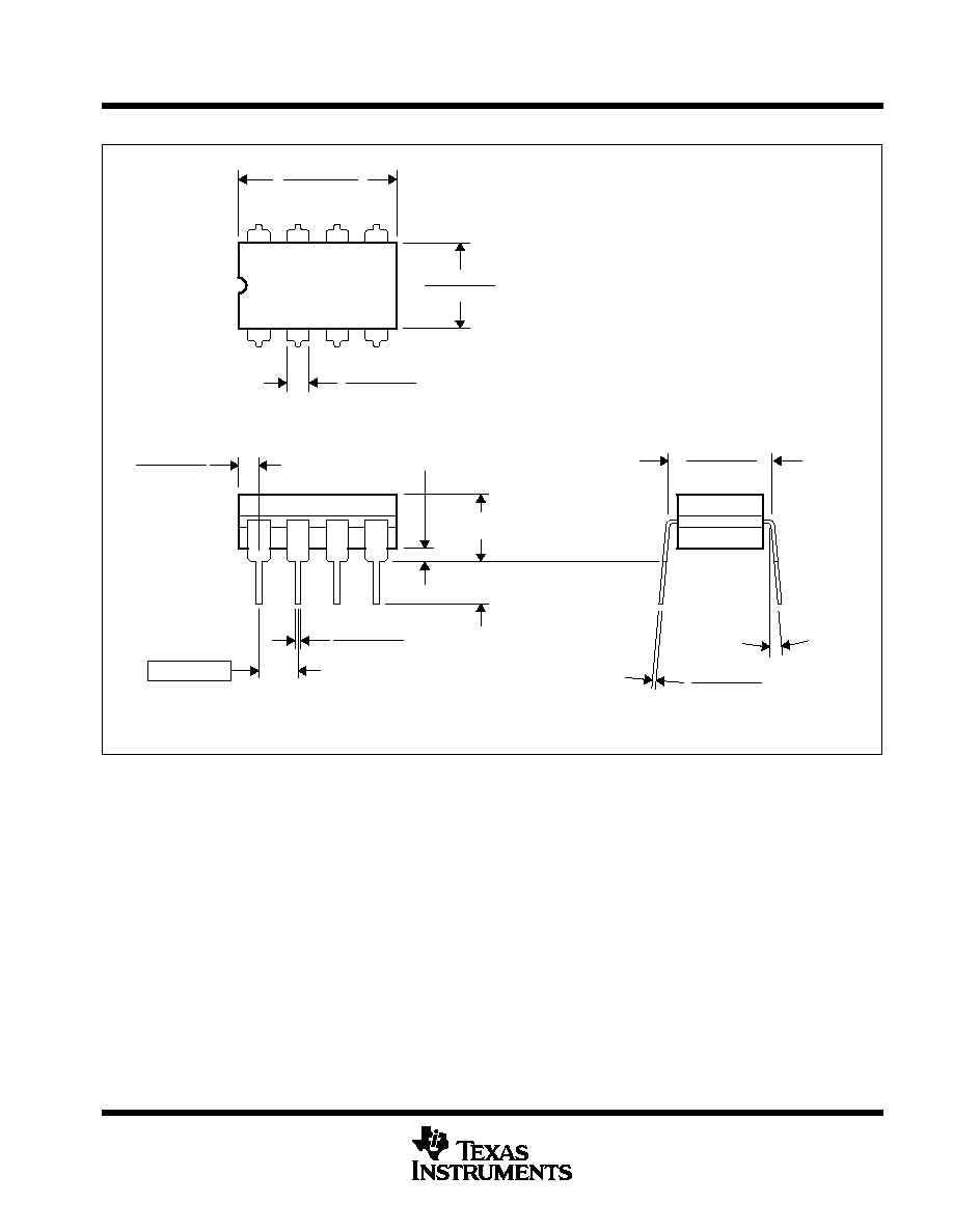
JG (R-GDIP-T8)
CERAMIC DUAL-IN-LINE
0.310 (7,87)
0.290 (7,37)
0.014 (0,36)
0.008 (0,20)
Seating Plane
4040107/C 08/96
5
4
0.065 (1,65)
0.045 (1,14)
8
1
0.020 (0,51) MIN
0.400 (10,16)
0.355 (9,00)
0.015 (0,38)
0.023 (0,58)
0.063 (1,60)
0.015 (0,38)
0.200 (5,08) MAX
0.130 (3,30) MIN
0.245 (6,22)
0.280 (7,11)
0.100 (2,54)
0
∞
≠15
∞
NOTES: A. All linear dimensions are in inches (millimeters).
B. This drawing is subject to change without notice.
C. This package can be hermetically sealed with a ceramic lid using glass frit.
D. Index point is provided on cap for terminal identification.
E. Falls within MIL STD 1835 GDIP1-T8

MECHANICAL DATA
MLCC006B ≠ OCTOBER 1996
1
POST OFFICE BOX 655303
∑
DALLAS, TEXAS 75265
FK (S-CQCC-N**)
LEADLESS CERAMIC CHIP CARRIER
4040140 / D 10/96
28 TERMINAL SHOWN
B
0.358
(9,09)
MAX
(11,63)
0.560
(14,22)
0.560
0.458
0.858
(21,8)
1.063
(27,0)
(14,22)
A
NO. OF
MIN
MAX
0.358
0.660
0.761
0.458
0.342
(8,69)
MIN
(11,23)
(16,26)
0.640
0.739
0.442
(9,09)
(11,63)
(16,76)
0.962
1.165
(23,83)
0.938
(28,99)
1.141
(24,43)
(29,59)
(19,32)
(18,78)
**
20
28
52
44
68
84
0.020 (0,51)
TERMINALS
0.080 (2,03)
0.064 (1,63)
(7,80)
0.307
(10,31)
0.406
(12,58)
0.495
(12,58)
0.495
(21,6)
0.850
(26,6)
1.047
0.045 (1,14)
0.045 (1,14)
0.035 (0,89)
0.035 (0,89)
0.010 (0,25)
12
13
14
15
16
18
17
11
10
8
9
7
5
4
3
2
0.020 (0,51)
0.010 (0,25)
6
1
28
26
27
19
21
B SQ
A SQ
22
23
24
25
20
0.055 (1,40)
0.045 (1,14)
0.028 (0,71)
0.022 (0,54)
0.050 (1,27)
NOTES: A. All linear dimensions are in inches (millimeters).
B. This drawing is subject to change without notice.
C. This package can be hermetically sealed with a metal lid.
D. The terminals are gold plated.
E. Falls within JEDEC MS-004
MECHANICAL DATA
MPDI001A ≠ JANUARY 1995 ≠ REVISED JUNE 1999
1
POST OFFICE BOX 655303
∑
DALLAS, TEXAS 75265
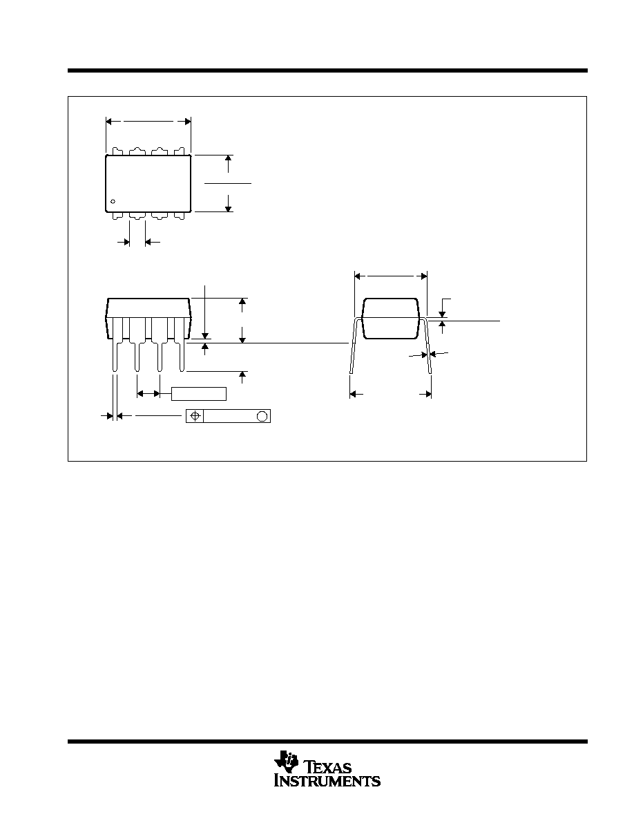
P (R-PDIP-T8)
PLASTIC DUAL-IN-LINE
8
4
0.015 (0,38)
Gage Plane
0.325 (8,26)
0.300 (7,62)
0.010 (0,25) NOM
MAX
0.430 (10,92)
4040082/D 05/98
0.200 (5,08) MAX
0.125 (3,18) MIN
5
0.355 (9,02)
0.020 (0,51) MIN
0.070 (1,78) MAX
0.240 (6,10)
0.260 (6,60)
0.400 (10,60)
1
0.015 (0,38)
0.021 (0,53)
Seating Plane
M
0.010 (0,25)
0.100 (2,54)
NOTES: A. All linear dimensions are in inches (millimeters).
B. This drawing is subject to change without notice.
C. Falls within JEDEC MS-001
For the latest package information, go to http://www.ti.com/sc/docs/package/pkg_info.htm
MECHANICAL DATA
MSOI002B ≠ JANUARY 1995 ≠ REVISED SEPTEMBER 2001
1
POST OFFICE BOX 655303
∑
DALLAS, TEXAS 75265
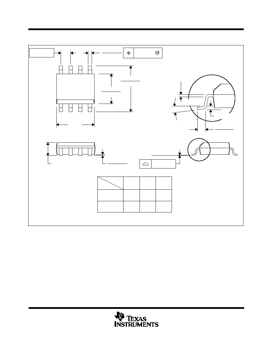
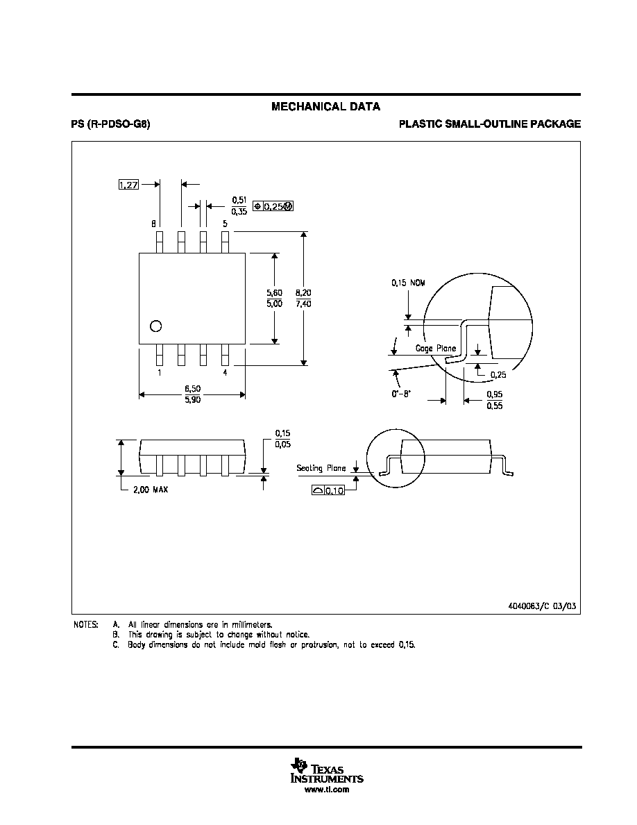
D (R-PDSO-G**)
PLASTIC SMALL-OUTLINE PACKAGE
8 PINS SHOWN
8
0.197
(5,00)
A MAX
A MIN
(4,80)
0.189
0.337
(8,55)
(8,75)
0.344
14
0.386
(9,80)
(10,00)
0.394
16
DIM
PINS **
4040047/E 09/01
0.069 (1,75) MAX
Seating Plane
0.004 (0,10)
0.010 (0,25)
0.010 (0,25)
0.016 (0,40)
0.044 (1,12)
0.244 (6,20)
0.228 (5,80)
0.020 (0,51)
0.014 (0,35)
1
4
8
5
0.150 (3,81)
0.157 (4,00)
0.008 (0,20) NOM
0
∞
≠ 8
∞
Gage Plane
A
0.004 (0,10)
0.010 (0,25)
0.050 (1,27)
NOTES: A. All linear dimensions are in inches (millimeters).
B. This drawing is subject to change without notice.
C. Body dimensions do not include mold flash or protrusion, not to exceed 0.006 (0,15).
D. Falls within JEDEC MS-012
MECHANICAL DATA
MTSS001C ≠ JANUARY 1995 ≠ REVISED FEBRUARY 1999
1
POST OFFICE BOX 655303
∑
DALLAS, TEXAS 75265
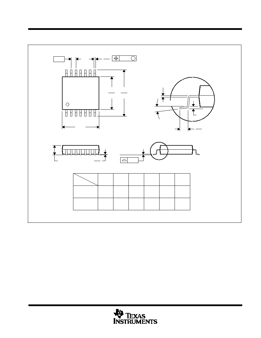
PW (R-PDSO-G**)
PLASTIC SMALL-OUTLINE PACKAGE
14 PINS SHOWN
0,65
M
0,10
0,10
0,25
0,50
0,75
0,15 NOM
Gage Plane
28
9,80
9,60
24
7,90
7,70
20
16
6,60
6,40
4040064/F 01/97
0,30
6,60
6,20
8
0,19
4,30
4,50
7
0,15
14
A
1
1,20 MAX
14
5,10
4,90
8
3,10
2,90
A MAX
A MIN
DIM
PINS **
0,05
4,90
5,10
Seating Plane
0
∞
≠ 8
∞
NOTES: A. All linear dimensions are in millimeters.
B. This drawing is subject to change without notice.
C. Body dimensions do not include mold flash or protrusion not to exceed 0,15.
D. Falls within JEDEC MO-153

IMPORTANT NOTICE
Texas Instruments Incorporated and its subsidiaries (TI) reserve the right to make corrections, modifications,
enhancements, improvements, and other changes to its products and services at any time and to discontinue
any product or service without notice. Customers should obtain the latest relevant information before placing
orders and should verify that such information is current and complete. All products are sold subject to TI's terms
and conditions of sale supplied at the time of order acknowledgment.
TI warrants performance of its hardware products to the specifications applicable at the time of sale in
accordance with TI's standard warranty. Testing and other quality control techniques are used to the extent TI
deems necessary to support this warranty. Except where mandated by government requirements, testing of all
parameters of each product is not necessarily performed.
TI assumes no liability for applications assistance or customer product design. Customers are responsible for
their products and applications using TI components. To minimize the risks associated with customer products
and applications, customers should provide adequate design and operating safeguards.
TI does not warrant or represent that any license, either express or implied, is granted under any TI patent right,
copyright, mask work right, or other TI intellectual property right relating to any combination, machine, or process
in which TI products or services are used. Information published by TI regarding third-party products or services
does not constitute a license from TI to use such products or services or a warranty or endorsement thereof.
Use of such information may require a license from a third party under the patents or other intellectual property
of the third party, or a license from TI under the patents or other intellectual property of TI.
Reproduction of information in TI data books or data sheets is permissible only if reproduction is without
alteration and is accompanied by all associated warranties, conditions, limitations, and notices. Reproduction
of this information with alteration is an unfair and deceptive business practice. TI is not responsible or liable for
such altered documentation.
Resale of TI products or services with statements different from or beyond the parameters stated by TI for that
product or service voids all express and any implied warranties for the associated TI product or service and
is an unfair and deceptive business practice. TI is not responsible or liable for any such statements.
Following are URLs where you can obtain information on other Texas Instruments products and application
solutions:
Products
Applications
Amplifiers
amplifier.ti.com
Audio
www.ti.com/audio
Data Converters
dataconverter.ti.com
Automotive
www.ti.com/automotive
DSP
dsp.ti.com
Broadband
www.ti.com/broadband
Interface
interface.ti.com
Digital Control
www.ti.com/digitalcontrol
Logic
logic.ti.com
Military
www.ti.com/military
Power Mgmt
power.ti.com
Optical Networking
www.ti.com/opticalnetwork
Microcontrollers
microcontroller.ti.com
Security
www.ti.com/security
Telephony
www.ti.com/telephony
Video & Imaging
www.ti.com/video
Wireless
www.ti.com/wireless
Mailing Address:
Texas Instruments
Post Office Box 655303 Dallas, Texas 75265
Copyright
2003, Texas Instruments Incorporated