SN54HC02, SN74HC02
QUADRUPLE 2-INPUT POSITIVE-NOR GATES
SCLS076E ≠ DECEMBER 1982 ≠ REVISED AUGUST 2003
1
POST OFFICE BOX 655303
∑
DALLAS, TEXAS 75265
D
Wide Operating Voltage Range of 2 V to 6 V
D
Outputs Can Drive Up To 10 LSTTL Loads
D
Low Power Consumption, 20-
µ
A Max I
CC
D
Typical t
pd
= 8 ns
D
±
4-mA Output Drive at 5 V
D
Low Input Current of 1
µ
A Max
1
2
3
4
5
6
7
14
13
12
11
10
9
8
1Y
1A
1B
2Y
2A
2B
GND
V
CC
4Y
4B
4A
3Y
3B
3A
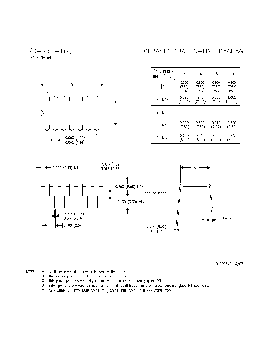
SN54HC02 . . . J OR W PACKAGE
SN74HC02 . . . D, DB, N, NS, OR PW PACKAGE
(TOP VIEW)
3
2 1 20 19
9 10 11 12 13
4
5
6
7
8
18
17
16
15
14
4B
NC
4A
NC
3Y
1B
NC
2Y
NC
2A
1A
1Y
NC
3A
3B
V
4Y
2B
GND
NC
SN54HC02 . . . FK PACKAGE
(TOP VIEW)
CC
NC ≠ No internal connection
description/ordering information
The 'HC02 devices contain four independent 2-input NOR gates. They perform the Boolean function
Y = A + B or Y = A
∑
B in positive logic.
ORDERING INFORMATION
TA
PACKAGE
ORDERABLE
PART NUMBER
TOP-SIDE
MARKING
≠40 C to 85 C
PDIP ≠ N
Tube of 25
SN74HC02N
SN74HC02N
≠40 C to 85 C
SOIC ≠ D
Tube of 50
SN74HC02D
HC02
≠40 C to 85 C
SOIC ≠ D
Reel of 2500
SN74HC02DR
HC02
≠40 C to 85 C
Reel of 250
SN74HC02DT
≠40
∞
C to 85
∞
C
SOP ≠ NS
Reel of 2000
SN74HC02NSR
HC02
SSOP ≠ DB
Reel of 2000
SN74HC02DBR
HC02
TSSOP ≠ PW
Tube of 90
SN74HC02PW
HC02
TSSOP ≠ PW
Reel of 2000
SN74HC02PWR
HC02
Reel of 250
SN74HC02PWT
≠55 C to 125 C
CDIP ≠ J
Tube of 25
SNJ54HC02J
SNJ54HC02J
≠55
∞
C to 125
∞
C
CFP ≠ W
Tube of 150
SNJ54HC02W
SNJ54HC02W
LCCC ≠ FK
Tube of 55
SNJ54HC02FK
SNJ54HC02FK
Package drawings, standard packing quantities, thermal data, symbolization, and PCB design guidelines are
available at www.ti.com/sc/package.
Please be aware that an important notice concerning availability, standard warranty, and use in critical applications of
Texas Instruments semiconductor products and disclaimers thereto appears at the end of this data sheet.
Copyright
2003, Texas Instruments Incorporated
PRODUCTION DATA information is current as of publication date.
Products conform to specifications per the terms of Texas Instruments
standard warranty. Production processing does not necessarily include
testing of all parameters.
On products compliant to MIL-PRF-38535, all parameters are tested
unless otherwise noted. On all other products, production
processing does not necessarily include testing of all parameters.
SN54HC02, SN74HC02
QUADRUPLE 2-INPUT POSITIVE-NOR GATES
SCLS076E ≠ DECEMBER 1982 ≠ REVISED AUGUST 2003
2
POST OFFICE BOX 655303
∑
DALLAS, TEXAS 75265
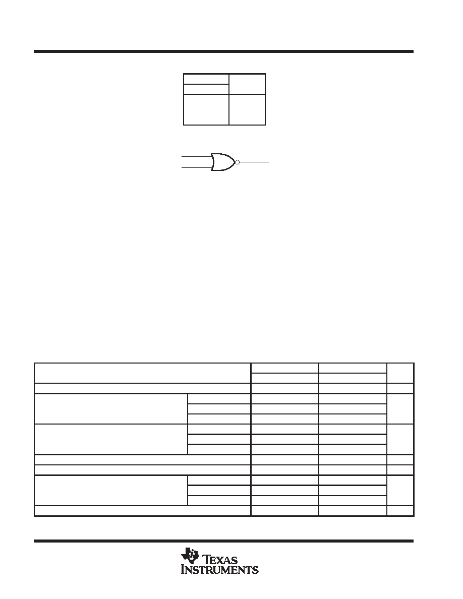
FUNCTION TABLE
(each gate)
INPUTS
OUTPUT
A
B
OUTPUT
Y
H
X
L
X
H
L
L
L
H
logic diagram (positive logic)
A
B
Y
absolute maximum ratings over operating free-air temperature range (unless otherwise noted)
Supply voltage range, V
CC
≠0.5 V to 7 V
. . . . . . . . . . . . . . . . . . . . . . . . . . . . . . . . . . . . . . . . . . . . . . . . . . . . . . . . . .
Input clamp current, I
IK
(V
I
< 0 or V
I
> V
CC
) (see Note 1)
±
20 mA
. . . . . . . . . . . . . . . . . . . . . . . . . . . . . . . . . . . .
Output clamp current, I
OK
(V
O
< 0 or V
O
> V
CC
) (see Note 1)
±
20 mA
. . . . . . . . . . . . . . . . . . . . . . . . . . . . . . . .
Continuous output current, I
O
(V
O
= 0 to V
CC
)
±
25 mA
. . . . . . . . . . . . . . . . . . . . . . . . . . . . . . . . . . . . . . . . . . . . . .
Continuous current through V
CC
or GND
±
50 mA
. . . . . . . . . . . . . . . . . . . . . . . . . . . . . . . . . . . . . . . . . . . . . . . . . . .
Package thermal impedance,
JA
(see Note 2): D package
86
∞
C/W
. . . . . . . . . . . . . . . . . . . . . . . . . . . . . . . . . . .
DB package
96
∞
C/W
. . . . . . . . . . . . . . . . . . . . . . . . . . . . . . . . .
N package
80
∞
C/W
. . . . . . . . . . . . . . . . . . . . . . . . . . . . . . . . . . .
NS package
76
∞
C/W
. . . . . . . . . . . . . . . . . . . . . . . . . . . . . . . . .
PW package
113
∞
C/W
. . . . . . . . . . . . . . . . . . . . . . . . . . . . . . . .
Storage temperature range, T
stg
≠65
∞
C to 150
∞
C
. . . . . . . . . . . . . . . . . . . . . . . . . . . . . . . . . . . . . . . . . . . . . . . . . . .
Stresses beyond those listed under "absolute maximum ratings" may cause permanent damage to the device. These are stress ratings only, and
functional operation of the device at these or any other conditions beyond those indicated under "recommended operating conditions" is not
implied. Exposure to absolute-maximum-rated conditions for extended periods may affect device reliability.
NOTES:
1. The input and output voltage ratings may be exceeded if the input and output current ratings are observed.
2. The package thermal impedance is calculated in accordance with JESD 51-7.
recommended operating conditions (see Note 3)
SN54HC02
SN74HC02
UNIT
MIN
NOM
MAX
MIN
NOM
MAX
UNIT
VCC
Supply voltage
2
5
6
2
5
6
V
V
High-level input voltage
VCC = 2 V
1.5
1.5
V
VIH
High-level input voltage
VCC = 4.5 V
3.15
3.15
V
IH
VCC = 6 V
4.2
4.2
V
Low-level input voltage
VCC = 2 V
0.5
0.5
V
VIL
Low-level input voltage
VCC = 4.5 V
1.35
1.35
V
IL
VCC = 6 V
1.8
1.8
VI
Input voltage
0
VCC
0
VCC
V
VO
Output voltage
0
VCC
0
VCC
V
t/ v
Input transition rise/fall time
VCC = 2 V
1000
1000
ns
t/
v
Input transition rise/fall time
VCC = 4.5 V
500
500
ns
VCC = 6 V
400
400
TA
Operating free-air temperature
≠55
125
≠40
85
∞
C
NOTE 3: All unused inputs of the device must be held at VCC or GND to ensure proper device operation. Refer to the TI application report,
Implications of Slow or Floating CMOS Inputs, literature number SCBA004.
SN54HC02, SN74HC02
QUADRUPLE 2-INPUT POSITIVE-NOR GATES
SCLS076E ≠ DECEMBER 1982 ≠ REVISED AUGUST 2003
3
POST OFFICE BOX 655303
∑
DALLAS, TEXAS 75265
electrical characteristics over recommended operating free-air temperature range (unless
otherwise noted)
PARAMETER
TEST CONDITIONS
VCC
TA = 25
∞
C
SN54HC02
SN74HC02
UNIT
PARAMETER
TEST CONDITIONS
VCC
MIN
TYP
MAX
MIN
MAX
MIN
MAX
UNIT
V
V = V
or V
I
= ≠20 A
2 V
1.9
1.998
1.9
1.9
V
V
V = V
or V
IOH = ≠20
µ
A
4.5 V
4.4
4.499
4.4
4.4
V
VOH
VI = VIH or VIL
OH
6 V
5.9
5.999
5.9
5.9
V
OH
I
IH
IL
IOH = ≠4 mA
4.5 V
3.98
4.3
3.7
3.84
IOH = ≠5.2 mA
6 V
5.48
5.8
5.2
5.34
V
V = V
or V
I
= 20 A
2 V
0.002
0.1
0.1
0.1
V
V
V = V
or V
IOL = 20
µ
A
4.5 V
0.001
0.1
0.1
0.1
V
VOL
VI = VIH or VIL
OL
6 V
0.001
0.1
0.1
0.1
V
OL
I
IH
IL
IOL = 4 mA
4.5 V
0.17
0.26
0.4
0.33
IOL = 5.2 mA
6 V
0.15
0.26
0.4
0.33
II
VI = VCC or 0
6 V
±
0.1
±
100
±
1000
±
1000
nA
ICC
VI = VCC or 0,
IO = 0
6 V
2
40
20
µ
A
Ci
2 V to 6 V
3
10
10
10
pF
switching characteristics over recommended operating free-air temperature range, C
L
= 50 pF
(unless otherwise noted) (see Figure 1)
PARAMETER
FROM
TO
VCC
TA = 25
∞
C
SN54HC02
SN74HC02
UNIT
PARAMETER
FROM
(INPUT)
TO
(OUTPUT)
VCC
MIN
TYP
MAX
MIN
MAX
MIN
MAX
UNIT
t
A or B
Y
2 V
45
90
135
115
ns
tpd
A or B
Y
4.5 V
9
18
27
23
ns
pd
6 V
8
15
23
20
t
Y
2 V
38
75
110
95
ns
tt
Y
4.5 V
8
15
22
19
ns
t
6 V
6
13
19
16
operating characteristics, T
A
= 25
∞
C
PARAMETER
TEST CONDITIONS
TYP
UNIT
Cpd
Power dissipation capacitance per gate
No load
22
pF
SN54HC02, SN74HC02
QUADRUPLE 2-INPUT POSITIVE-NOR GATES
SCLS076E ≠ DECEMBER 1982 ≠ REVISED AUGUST 2003
4
POST OFFICE BOX 655303
∑
DALLAS, TEXAS 75265
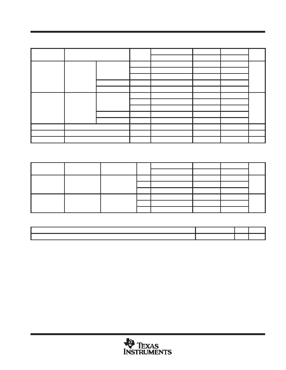
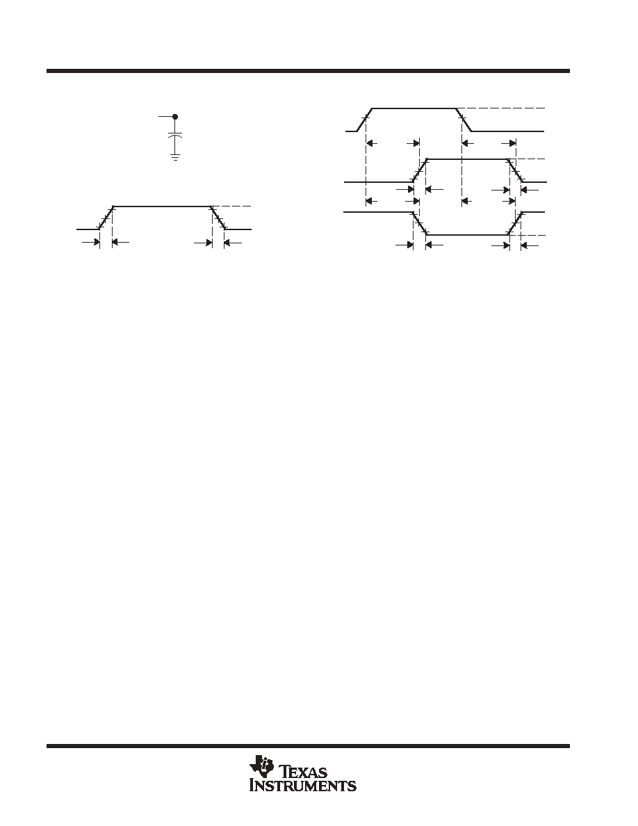
PARAMETER MEASUREMENT INFORMATION
VOLTAGE WAVEFORM
INPUT RISE AND FALL TIMES
50%
50%
10%
10%
90%
90%
VCC
0 V
tr
tf
Input
VOLTAGE WAVEFORMS
PROPAGATION DELAY AND OUTPUT TRANSITION TIMES
50%
50%
50%
10%
10%
90%
90%
VCC
VOH
VOL
0 V
tr
tf
Input
In-Phase
Output
50%
tPLH
tPHL
50%
50%
10%
10%
90%
90%
VOH
VOL
tr
tf
tPHL
tPLH
Out-of-Phase
Output
Test
Point
From Output
Under Test
CL = 50 pF
(see Note A)
LOAD CIRCUIT
NOTES: A. CL includes probe and test-fixture capacitance.
B. Phase relationships between waveforms were chosen arbitrarily. All input pulses are supplied by generators having the following
characteristics: PRR
1 MHz, ZO = 50
, tr = 6 ns, tf = 6 ns.
C. The outputs are measured one at a time with one input transition per measurement.
D. tPLH and tPHL are the same as tpd.
Figure 1. Load Circuit and Voltage Waveforms