 | –≠–ª–µ–∫—Ç—Ä–æ–Ω–Ω—ã–π –∫–æ–º–ø–æ–Ω–µ–Ω—Ç: L123ATQ | –°–∫–∞—á–∞—Ç—å:  PDF PDF  ZIP ZIP |

SN74LV123A Q1
DUAL RETRIGGERABLE MONOSTABLE MULTIVIBRATOR
WITH SCHMITT TRIGGER INPUTS
SCLS467B - FEBRUARY 2003 - REVISED MAY 2004
1
POST OFFICE BOX 655303
∑
DALLAS, TEXAS 75265
D
Qualification in Accordance With
AEC-Q100
D
Qualified for Automotive Applications
D
Customer-Specific Configuration Control
Can Be Supported Along With
Major-Change Approval
D
Typical V
OLP
(Output Ground Bounce)
<0.8 V at V
CC
= 3.3 V, T
A
= 25
∞
C
D
Typical V
OHV
(Output V
OH
Undershoot)
>2.3 V at V
CC
= 3.3 V, T
A
= 25
∞
C
D
Supports Mixed-Mode Voltage Operation on
All Ports
D
Schmitt-Trigger Circuitry on A, B, and CLR
Inputs for Slow Input Transition Rates
D
Edge Triggered From Active-High or
Active-Low Gated Logic Inputs
D
I
off
Supports Partial-Power-Down Mode
Operation
D
Retriggerable for Very Long Output Pulses,
Up To 100% Duty Cycle
D
Overriding Clear Terminates Output Pulse
D
Glitch-Free Power-Up Reset on Outputs
D
ESD Protection Exceeds JESD 22
- 2000-V Human-Body Model (A114-A)
- 200-V Machine Model (A115-A)
- 1000-V Charged-Device Model (C101)
Contact factory for details. Q100 qualification data available on
request.
description/ordering information
The SN74LV123A is a dual retriggerable monostable multivibrator designed for 2-V to 5.5-V V
CC
operation.
This edge-triggered multivibrator features output pulse-duration control by three methods. In the first method,
the A input is low, and the B input goes high. In the second method, the B input is high, and the A input goes
low. In the third method, the A input is low, the B input is high, and the clear (CLR) input goes high.
The output pulse duration is programmable by selecting external resistance and capacitance values. The
external timing capacitor must be connected between C
ext
and R
ext
/C
ext
(positive) and an external resistor
connected between R
ext
/C
ext
and V
CC
. To obtain variable pulse durations, connect an external variable
resistance between R
ext
/C
ext
and V
CC
. The output pulse duration also can be reduced by taking CLR low.
ORDERING INFORMATION
TA
PACKAGE
ORDERABLE
PART NUMBER
TOP-SIDE
MARKING
-40
∞
C to 105
∞
C
TSSOP - PW
Tape and reel
SN74LV123ATPWRQ1
L123ATQ
Package drawings, standard packing quantities, thermal data, symbolization, and PCB design
guidelines are available at www.ti.com/sc/package.
Copyright
2004, Texas Instruments Incorporated
Please be aware that an important notice concerning availability, standard warranty, and use in critical applications of
Texas Instruments semiconductor products and disclaimers thereto appears at the end of this data sheet.
PW PACKAGE
(TOP VIEW)
1
2
3
4
5
6
7
8
16
15
14
13
12
11
10
9
1A
1B
1CLR
1Q
2Q
2C
ext
2R
ext
/C
ext
GND
V
CC
1R
ext
/C
ext
1C
ext
1Q
2Q
2CLR
2B
2A
PRODUCTION DATA information is current as of publication date.
Products conform to specifications per the terms of Texas Instruments
standard warranty. Production processing does not necessarily include
testing of all parameters.

SN74LV123A Q1
DUAL RETRIGGERABLE MONOSTABLE MULTIVIBRATOR
WITH SCHMITT TRIGGER INPUTS
SCLS467B - FEBRUARY 2003 - REVISED MAY 2004
2
POST OFFICE BOX 655303
∑
DALLAS, TEXAS 75265
description/ordering information (continued)
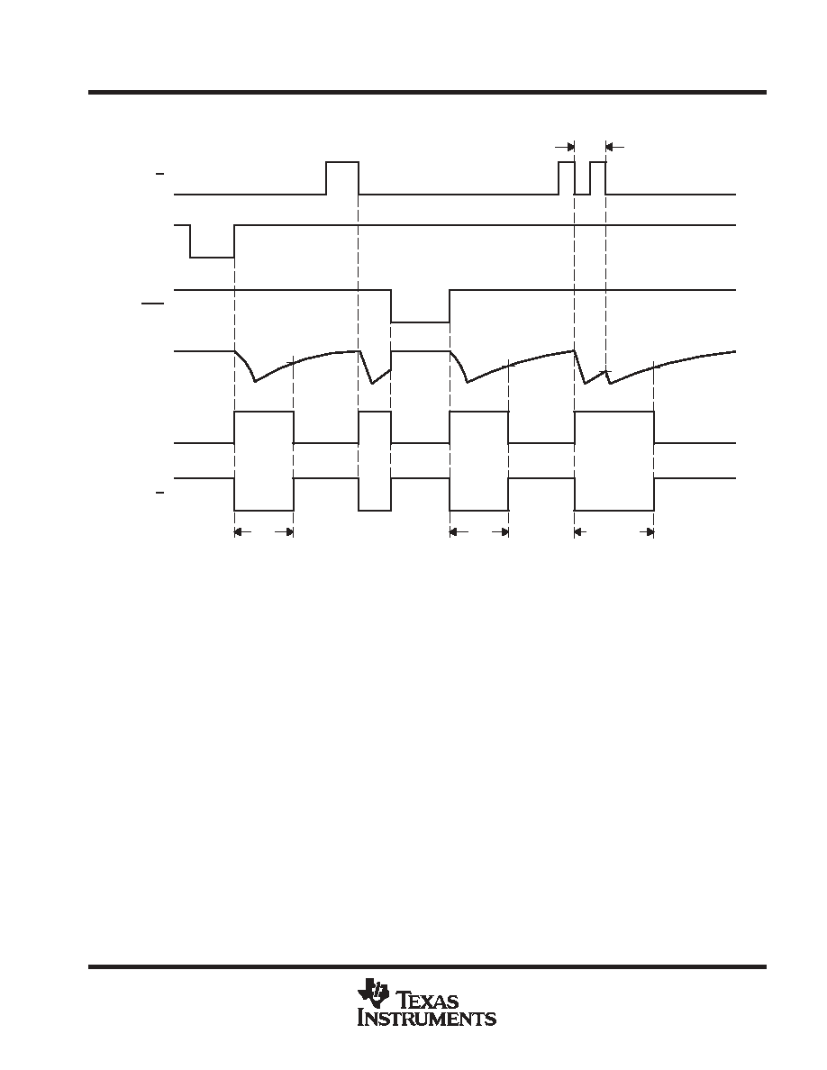
Pulse triggering occurs at a particular voltage level and is not directly related to the transition time of the input
pulse. The A, B, and CLR inputs have Schmitt triggers with sufficient hysteresis to handle slow input transition
rates with jitter-free triggering at the outputs.
Once triggered, the basic pulse duration can be extended by retriggering the gated low-level-active (A) or
high-level-active (B) input. Pulse duration can be reduced by taking CLR low. The input/output timing diagram
illustrates pulse control by retriggering the inputs and early clearing.
During power up, Q outputs are in the low state, and Q outputs are in the high state. The outputs are glitch free,
without applying a reset pulse.
This device is fully specified for partial-power-down applications using I
off
. The I
off
circuitry disables the outputs,
preventing damaging current backflow through the device when it is powered down.
FUNCTION TABLE
(each multivibrator)
INPUTS
OUTPUTS
CLR
A
B
Q
Q
L
X
X
L
H
X
H
X
L
H
X
X
L
L
H
H
L
H
H
L
H
These outputs are based on the
assumption that the indicated
steady-state conditions at the A and
B inputs have been set up long enough to
complete any pulse started before the
setup.
logic diagram, each multivibrator (positive logic)
CLR
Cext
Rext/Cext
R
B
A
Q
Q
SN74LV123A Q1
DUAL RETRIGGERABLE MONOSTABLE MULTIVIBRATOR
WITH SCHMITT TRIGGER INPUTS
SCLS467B - FEBRUARY 2003 - REVISED MAY 2004
3
POST OFFICE BOX 655303
∑
DALLAS, TEXAS 75265
input/output timing diagram
A
B
CLR
Q
Q
tw
tw
tw + trr
trr
Rext/Cext
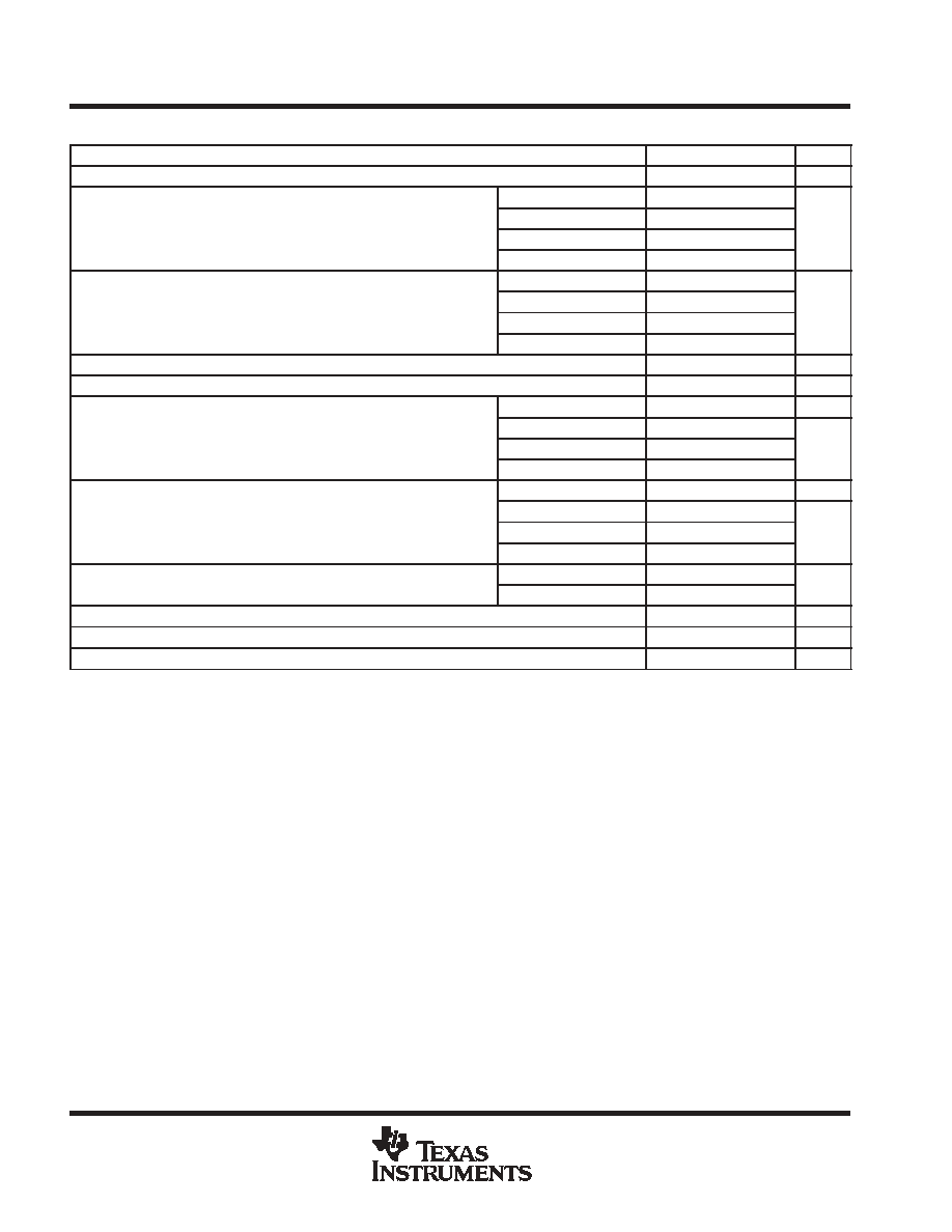
absolute maximum ratings over operating free-air temperature (unless otherwise noted)
Supply voltage range, V
CC
-0.5 V to 7 V
. . . . . . . . . . . . . . . . . . . . . . . . . . . . . . . . . . . . . . . . . . . . . . . . . . . . . . . . . .
Input voltage range, V
I
(see Note 1)
-0.5 V to 7 V
. . . . . . . . . . . . . . . . . . . . . . . . . . . . . . . . . . . . . . . . . . . . . . . . . .
Voltage range applied to any output in the high-impedance
or power-off state, V
O
(see Note 1)
-0.5 V to 7 V
. . . . . . . . . . . . . . . . . . . . . . . . . . . . . . . . . . . . . . . . . . . . . . . .
Output voltage range in high or low state, V
O
(see Notes 1 and 2)
-0.5 V to V
CC
+ 0.5 V
. . . . . . . . . . . . . . . . .
Output voltage range in power-off state, V
O
(see Note 1)
-0.5 V to 7 V
. . . . . . . . . . . . . . . . . . . . . . . . . . . . . . . .
Input clamp current, I
IK
(V
I
< 0)
-20 mA
. . . . . . . . . . . . . . . . . . . . . . . . . . . . . . . . . . . . . . . . . . . . . . . . . . . . . . . . . . .
Output clamp current, I
OK
(V
O
< 0)
-50 mA
. . . . . . . . . . . . . . . . . . . . . . . . . . . . . . . . . . . . . . . . . . . . . . . . . . . . . . . .
Continuous output current, I
O
(V
O
= 0 to V
CC
)
±
25 mA
. . . . . . . . . . . . . . . . . . . . . . . . . . . . . . . . . . . . . . . . . . . . . .
Continuous current through V
CC
or GND
±
50 mA
. . . . . . . . . . . . . . . . . . . . . . . . . . . . . . . . . . . . . . . . . . . . . . . . . . .
Package thermal impedance,
JA
(see Note 3)
113
∞
C/W
. . . . . . . . . . . . . . . . . . . . . . . . . . . . . . . . . . . . . . . . . . . .
Storage temperature range, T
stg
-65
∞
C to 150
∞
C
. . . . . . . . . . . . . . . . . . . . . . . . . . . . . . . . . . . . . . . . . . . . . . . . . . .
Stresses beyond those listed under "absolute maximum ratings" may cause permanent damage to the device. These are stress ratings only, and
functional operation of the device at these or any other conditions beyond those indicated under "recommended operating conditions" is not
implied. Exposure to absolute-maximum-rated conditions for extended periods may affect device reliability.
NOTES:
1. The input and output negative-voltage ratings may be exceeded if the input and output current ratings are observed.
2. This value is limited to 5.5 V maximum.
3. The package thermal impedance is calculated in accordance with JESD 51-7.
SN74LV123A Q1
DUAL RETRIGGERABLE MONOSTABLE MULTIVIBRATOR
WITH SCHMITT TRIGGER INPUTS
SCLS467B - FEBRUARY 2003 - REVISED MAY 2004
4
POST OFFICE BOX 655303
∑
DALLAS, TEXAS 75265
recommended operating conditions (see Note 4)
MIN
MAX
UNIT
VCC
Supply voltage
2
5.5
V
VCC = 2 V
1.5
VIH
High-level input voltage
VCC = 2.3 V to 2.7 V
VCC
◊
0.7
V
VIH
High-level input voltage
VCC = 3 V to 3.6 V
VCC
◊
0.7
V
VCC = 4.5 V to 5.5 V
VCC
◊
0.7
VCC = 2 V
0.5
VIL
Low-level input voltage
VCC = 2.3 V to 2.7 V
VCC
◊
0.3
V
VIL
Low-level input voltage
VCC = 3 V to 3.6 V
VCC
◊
0.3
V
VCC = 4.5 V to 5.5 V
VCC
◊
0.3
VI
Input voltage
0
5.5
V
VO
Output voltage
0
VCC
V
VCC = 2 V
-50
µ
A
IOH
High-level output current
VCC = 2.3 V to 2.7 V
-2
IOH
High-level output current
VCC = 3 V to 3.6 V
-6
mA
VCC = 4.5 V to 5.5 V
-12
mA
VCC = 2 V
50
µ
A
IOL
Low-level output current
VCC = 2.3 V to 2.7 V
2
IOL
Low-level output current
VCC = 3 V to 3.6 V
6
mA
VCC = 4.5 V to 5.5 V
12
mA
Rext
External timing resistance
VCC = 2 V
5
k
Rext
External timing resistance
VCC
3 V
1
k
Cext
External timing capacitance
No restriction
pF
t/
VCC
Power-up ramp rate
1
ms/V
TA
Operating free-air temperature
-40
105
∞
C
NOTE 4: All unused inputs of the device must be held at VCC or GND to ensure proper device operation. Refer to the TI application report,
Implications of Slow or Floating CMOS Inputs, literature number SCBA004.
SN74LV123A Q1
DUAL RETRIGGERABLE MONOSTABLE MULTIVIBRATOR
WITH SCHMITT TRIGGER INPUTS
SCLS467B - FEBRUARY 2003 - REVISED MAY 2004
5
POST OFFICE BOX 655303
∑
DALLAS, TEXAS 75265
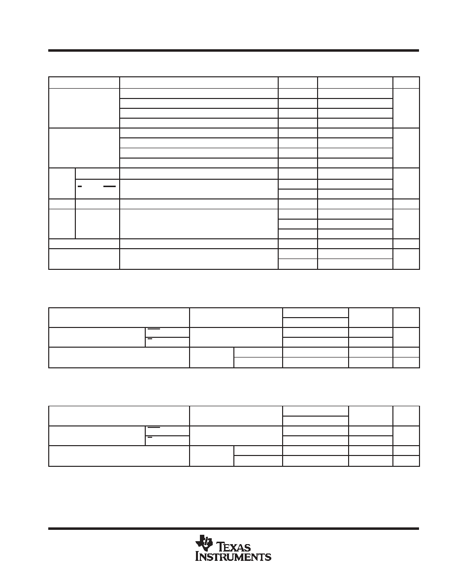
electrical characteristics over recommended operating free-air temperature range (unless
otherwise noted)
PARAMETER
TEST CONDITIONS
VCC
MIN
TYP
MAX
UNIT
IOH = -50
µ
A
2 V to 5.5 V
VCC-0.1
VOH
IOH = -2 mA
2.3 V
2
V
VOH
IOH = -6 mA
3 V
2.48
V
IOH = -12 mA
4.5 V
3.8
IOL = 50
µ
A
2 V to 5.5 V
0.1
VOL
IOL = 2 mA
2.3 V
0.4
V
VOL
IOL = 6 mA
3 V
0.44
V
IOL = 12 mA
4.5 V
0.55
Rext/Cext
VI = 5.5 V or GND
2 V to 5.5 V
±
2.5
II
A, B, and CLR
VI = 5.5 V or GND
0
±
1
µ
A
II
A, B, and CLR
VI = 5.5 V or GND
0 to 5.5 V
±
1
µ
A
ICC
Quiescent
VI = VCC or GND,
IO = 0
5.5 V
20
µ
A
Active state
VI = VCC or GND,
3 V
280
ICC
Active state
(per circuit)
VI = VCC or GND,
Rext/Cext = 0.5 VCC
4.5 V
650
µ
A
ICC
(per circuit)
Rext/Cext = 0.5 VCC
5.5 V
975
µ
A
Ioff
VI or VO = 0 to 5.5 V
0
5
µ
A
Ci
VI = VCC or GND
3.3 V
1.9
pF
Ci
VI = VCC or GND
5 V
1.9
pF
This test is performed with the terminal in the off-state condition.
timing requirements over recommended operating free-air temperature range, V
CC
= 3.3 V
±
0.3 V
(unless otherwise noted) (see Figure 1)
TEST CONDITIONS
TA = 25
∞
C
MIN
MAX
UNIT
TEST CONDITIONS
MIN
TYP
MAX
MIN
MAX
UNIT
tw
Pulse
CLR
5
5
ns
tw
Pulse
duration
A or B trigger
5
5
ns
trr
Pulse retrigger time
Rext = 1 k
Cext = 100 pF
76
ns
trr
Pulse retrigger time
Rext = 1 k
Cext = 0.01
µ
F
1.8
µ
s
See retriggering data in the application information section.
timing requirements over recommended operating free-air temperature range, V
CC
= 5 V
±
0.5 V
(unless otherwise noted) (see Figure 1)
TEST CONDITIONS
TA = 25
∞
C
MIN
MAX
UNIT
TEST CONDITIONS
MIN
TYP
MAX
MIN
MAX
UNIT
tw
Pulse
CLR
5
5
ns
tw
Pulse
duration
A or B trigger
5
5
ns
trr
Pulse retrigger time
Rext = 1 k
Cext = 100 pF
59
ns
trr
Pulse retrigger time
Rext = 1 k
Cext = 0.01
µ
F
1.5
µ
s
See retriggering data in the application information section.