
LM111, LM211, LM311
DIFFERENTIAL COMPARATORS WITH STROBES
SLCS007H ≠ SEPTEMBER 1973 ≠ REVISED AUGUST 2003
1
POST OFFICE BOX 655303
∑
DALLAS, TEXAS 75265
D
Fast Response Times
D
Strobe Capability
D
Maximum Input Bias Current . . . 300 nA
D
Maximum Input Offset Current . . . 70 nA
D
Can Operate From Single 5-V Supply
D
Available in Q-Temp Automotive
≠ High-Reliability Automotive Applications
≠ Configuration Control/Print Support
≠ Qualification to Automotive Standards
1
2
3
4
8
7
6
5
EMIT OUT
IN+
IN≠
V
CC≠
V
CC+
COL OUT
BAL/STRB
BALANCE
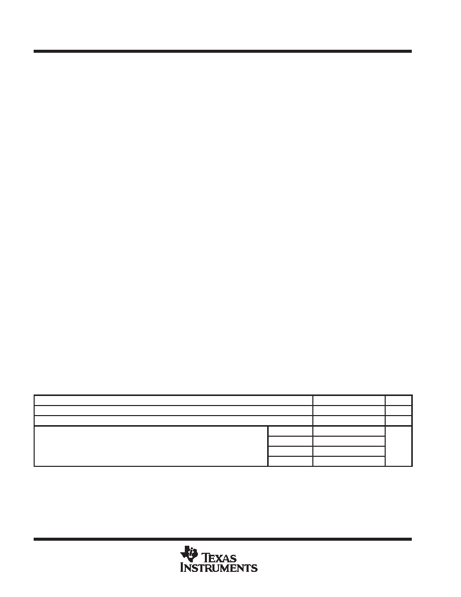
LM111 . . . JG PACKAGE
LM211 . . . D, P, OR PW PACKAGE
LM311 . . . D, P, PS, OR PW PACKAGE
(TOP VIEW)
3
2
1 20 19
9 10 11 12 13
4
5
6
7
8
18
17
16
15
14
NC
COL OUT
NC
BAL/STRB
NC
NC
IN+
NC
IN≠
NC
LM111 . . . FK PACKAGE
(TOP VIEW)
NC
EMIT
OUT
NC
BALANCE
NC
NC
NC
NC
CC≠
V
CC+
V
NC ≠ No internal connection
description/ordering information
The LM111, LM211, and LM311 are single high-speed voltage comparators. These devices are designed to
operate from a wide range of power-supply voltages, including
±
15-V supplies for operational amplifiers and
5-V supplies for logic systems. The output levels are compatible with most TTL and MOS circuits. These
comparators are capable of driving lamps or relays and switching voltages up to 50 V at 50 mA. All inputs and
outputs can be isolated from system ground. The outputs can drive loads referenced to ground, V
CC+
or V
CC≠
.
Offset balancing and strobe capabilities are available, and the outputs can be wire-OR connected. If the strobe
is low, the output is in the off state, regardless of the differential input.
Please be aware that an important notice concerning availability, standard warranty, and use in critical applications of
Texas Instruments semiconductor products and disclaimers thereto appears at the end of this data sheet.
Copyright
2003, Texas Instruments Incorporated
PRODUCTION DATA information is current as of publication date.
Products conform to specifications per the terms of Texas Instruments
standard warranty. Production processing does not necessarily include
testing of all parameters.
On products compliant to MIL-PRF-38535, all parameters are tested
unless otherwise noted. On all other products, production
processing does not necessarily include testing of all parameters.
LM111, LM211, LM311
DIFFERENTIAL COMPARATORS WITH STROBES
SLCS007H ≠ SEPTEMBER 1973 ≠ REVISED AUGUST 2003
4
POST OFFICE BOX 655303
∑
DALLAS, TEXAS 75265
absolute maximum ratings over operating free-air temperature range (unless otherwise noted)
Supply voltage: V
CC+
(see Note 1)
18 V
. . . . . . . . . . . . . . . . . . . . . . . . . . . . . . . . . . . . . . . . . . . . . . . . . . . . . . . . . . .
V
CC≠
(see Note 1)
≠18 V
. . . . . . . . . . . . . . . . . . . . . . . . . . . . . . . . . . . . . . . . . . . . . . . . . . . . . . . . . .
V
CC+
≠ V
CC≠
36 V
. . . . . . . . . . . . . . . . . . . . . . . . . . . . . . . . . . . . . . . . . . . . . . . . . . . . . . . . . . . . . . .
Differential input voltage, V
ID
(see Note 2)
±
30 V
. . . . . . . . . . . . . . . . . . . . . . . . . . . . . . . . . . . . . . . . . . . . . . . . . . .
Input voltage, V
I
(either input, see Notes 1 and 3)
±
15 V
. . . . . . . . . . . . . . . . . . . . . . . . . . . . . . . . . . . . . . . . . . . . .
Voltage from emitter output to V
CC≠
30
V
. . . . . . . . . . . . . . . . . . . . . . . . . . . . . . . . . . . . . . . . . . . . . . . . . . . . . . . . . .
Voltage from collector output to V
CC≠
: LM111 50
V
. . . . . . . . . . . . . . . . . . . . . . . . . . . . . . . . . . . . . . . . . . . . . . . . .
LM211 50
V
. . . . . . . . . . . . . . . . . . . . . . . . . . . . . . . . . . . . . . . . . . . . . . . . .
LM211Q 50
V
. . . . . . . . . . . . . . . . . . . . . . . . . . . . . . . . . . . . . . . . . . . . . . .
LM311 40
V
. . . . . . . . . . . . . . . . . . . . . . . . . . . . . . . . . . . . . . . . . . . . . . . . .
Duration of output short circuit (see Note 4)
10 s
. . . . . . . . . . . . . . . . . . . . . . . . . . . . . . . . . . . . . . . . . . . . . . . . . . .
Package thermal impedance,
JA
(see Notes 5 and 6): D package
97
∞
C/W
. . . . . . . . . . . . . . . . . . . . . . . . . . . .
P package
85
∞
C/W
. . . . . . . . . . . . . . . . . . . . . . . . . . . .
PS package
95
∞
C/W
. . . . . . . . . . . . . . . . . . . . . . . . . . .
PW package
149
∞
C/W
. . . . . . . . . . . . . . . . . . . . . . . . .
Package thermal impedance,
JC
(see Notes 7 and 8): FK package
5.61
∞
C/W
. . . . . . . . . . . . . . . . . . . . . . . . .
JG package
14.5
∞
C/W
. . . . . . . . . . . . . . . . . . . . . . . . .
Operating virtual junction temperature, T
J
150
∞
C
. . . . . . . . . . . . . . . . . . . . . . . . . . . . . . . . . . . . . . . . . . . . . . . . . . .
Case temperature for 60 seconds: FK package
260
∞
C
. . . . . . . . . . . . . . . . . . . . . . . . . . . . . . . . . . . . . . . . . . . . . .
Lead temperature 1,6 mm (1/16 inch) from case for 10 seconds: J or JG package
300
∞
C
. . . . . . . . . . . . . . . .
Lead temperature 1,6 mm (1/16 inch) from case for 60 seconds: D, P, PS, or PW package
260
∞
C
. . . . . . . .
Storage temperature range, T
stg
≠65
∞
C to 150
∞
C
. . . . . . . . . . . . . . . . . . . . . . . . . . . . . . . . . . . . . . . . . . . . . . . . . . .
Stresses beyond those listed under "absolute maximum ratings" may cause permanent damage to the device. These are stress ratings only, and
functional operation of the device at these or any other conditions beyond those indicated under "recommended operating conditions" is not
implied. Exposure to absolute-maximum-rated conditions for extended periods may affect device reliability.
NOTES:
1. All voltage values, unless otherwise noted, are with respect to the midpoint between VCC+ and VCC≠.
2. Differential voltages are at IN+ with respect to IN≠.
3. The magnitude of the input voltage must never exceed the magnitude of the supply voltage or
±
15 V, whichever is less.
4. The output may be shorted to ground or either power supply.
5. Maximum power dissipation is a function of TJ(max),
JA, and TA. The maximum allowable power dissipation at any allowable
ambient temperature is PD = (TJ(max) ≠ TA)/
JA. Operating at the absolute maximum TJ of 150
∞
C can affect reliability.
6. The package thermal impedance is calculated in accordance with JESD 51-7.
7. Maximum power dissipation is a function of TJ(max),
JC, and TC. The maximum allowable power dissipation at any allowable case
temperature is PD = (TJ(max) ≠ TC)/
JC. Operating at the absolute maximum TJ of 150
∞
C can affect reliability.
8. The package thermal impedance is calculated in accordance with MIL-STD-883.
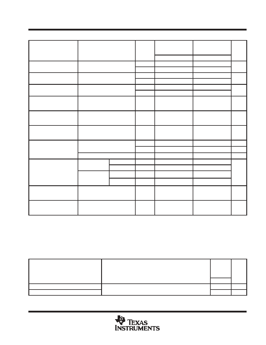
recommended operating conditions
MIN
MAX
UNIT
VCC+ ≠ VCC≠
Supply voltage
3.5
30
V
VI
Input voltage (|VCC
±
|
15 V)
VCC≠+0.5
VCC+≠1.5
V
T
Operating free-air temperature range
LM111
≠55
125
C
TA
Operating free-air temperature range
LM211
≠40
85
∞
C
TA
Operating free-air temperature range
LM211Q
≠40
125
∞
C
LM311
0
70
LM111, LM211, LM311
DIFFERENTIAL COMPARATORS WITH STROBES
SLCS007H ≠ SEPTEMBER 1973 ≠ REVISED AUGUST 2003
5
POST OFFICE BOX 655303
∑
DALLAS, TEXAS 75265
electrical characteristics at specified free-air temperature, V
CC
±
=
±
15 V (unless otherwise noted)
PARAMETER
TEST CONDITIONS
TA
LM111
LM211
LM211Q
LM311
UNIT
MIN
TYP
MAX
MIN
TYP
MAX
VIO
Input offset voltage
See Note 6
25
∞
C
0.7
3
2
7.5
mV
VIO
Input offset voltage
See Note 6
Full range
4
10
mV
IIO
Input offset current
See Note 6
25
∞
C
4
10
6
50
nA
IIO
Input offset current
See Note 6
Full range
20
70
nA
IIB
Input bias current
VO = 1 V to 14 V
25
∞
C
75
100
100
250
nA
IIB
Input bias current
VO = 1 V to 14 V
Full range
150
300
nA
IIL(S)
Low-level
strobe current
(see Note 7)
V(strobe) = 0.3 V,
VID
≠10 mV
25
∞
C
≠3
≠3
mA
VICR
Common-mode
input voltage range
Full range
13
to
≠14.5
13.8
to
≠14.7
13
to
≠14.5
13.8
to
≠14.7
V
AVD
Large-signal
differential voltage
amplification
VO = 5 V to 35 V,
RL = 1 k
25
∞
C
40
200
40
200
V/mV
I
High-level
(collector)
I(strobe) = ≠3 mA, VOH = 35 V,
25
∞
C
0.2
10
nA
IOH
(collector)
output leakage
I(strobe) = ≠3 mA,
VID = 5 mV
VOH = 35 V,
Full range
0.5
µ
A
OH
output leakage
current
VID = 5 mV,
VOH = 35 V
25
∞
C
0.2
50
nA
V
Low-level
IOL = 50 mA
VID = ≠5 mV
25
∞
C
0.75
1.5
V
V
Low-level
(collector-to-emitter)
IOL = 50 mA
VID = ≠10 mV
25
∞
C
0.75
1.5
V
VOL
Low-level
(collector-to-emitter)
output voltage
VCC+ = 4.5 V,
VCC≠ = 0,
VID = ≠6 mV
Full range
0.23
0.4
V
output voltage
VCC≠ = 0,
IOL = 8 mA
VID = ≠10 mV
Full range
0.23
0.4
ICC+
Supply current
from VCC+,
output low
VID = ≠10 mV,
No load
25
∞
C
5.1
6
5.1
7.5
mA
ICC≠
Supply current
from VCC≠,
output high
VID = 10 mV,
No load
25
∞
C
≠4.1
≠5
≠4.1
≠5
mA
Unless otherwise noted, all characteristics are measured with BALANCE and BAL/STRB open and EMIT OUT grounded.
Full range for LM111 is ≠55
∞
C to 125
∞
C, for LM211 is ≠40
∞
C to 85
∞
C, for LM211Q is ≠40
∞
C to 125
∞
C, and for LM311 is 0
∞
C to 70
∞
C.
All typical values are at TA = 25
∞
C.
NOTES:
9. The offset voltages and offset currents given are the maximum values required to drive the collector output up to 14 V or down to
1 V with a pullup resistor of 7.5 k
to VCC+. These parameters actually define an error band and take into account the worst-case
effects of voltage gain and input impedance.
10. The strobe should not be shorted to ground; it should be current driven at ≠3 mA to ≠5 mA (see Figures 13 and 27).
switching characteristics, V
CC
±
=
±
15 V, T
A
= 25
∞
C
PARAMETER
TEST CONDITIONS
LM111
LM211
LM211Q
LM311
UNIT
TYP
Response time, low-to-high-level output
RC = 500
to 5 V,
CL = 5 pF,
See Note 8
115
ns
Response time, high-to-low-level output
RC = 500
to 5 V,
CL = 5 pF,
See Note 8
165
ns
NOTE 11: The response time specified is for a 100-mV input step with 5-mV overdrive and is the interval between the input step function and the
instant when the output crosses 1.4 V.

