 | –≠–ª–µ–∫—Ç—Ä–æ–Ω–Ω—ã–π –∫–æ–º–ø–æ–Ω–µ–Ω—Ç: LM139AJB | –°–∫–∞—á–∞—Ç—å:  PDF PDF  ZIP ZIP |
LM139, LM139A, LM239, LM239A,
LM339, LM339A, LM2901, LM2901V
QUAD DIFFERENTIAL COMPARATORS
SLCS006L - OCTOBER 1979 - REVISED JUNE 2004
1
POST OFFICE BOX 655303
∑
DALLAS, TEXAS 75265
D
Single Supply or Dual Supplies
D
Wide Range of Supply Voltage:
- Max Rating . . . 2 V to 36 V
- Tested to 30 V . . . Non-V Devices
- Tested to 32 V . . . V-Suffix Devices
D
Low Supply-Current Drain Independent of
Supply Voltage . . . 0.8 mA Typ
D
Low Input Bias Current . . . 25 nA Typ
D
Low Input Offset Current . . . 3 nA Typ
(LM139)
D
Low Input Offset Voltage . . . 2 mV Typ
D
Common-Mode Input Voltage Range
Includes Ground
D
Differential Input Voltage Range Equal to
Maximum-Rated Supply Voltage . . .
±
36 V
D
Low Output Saturation Voltage
D
Output Compatible With TTL, MOS, and
CMOS
description/ordering information
These devices consist of four independent
voltage comparators that are designed to operate
from a single power supply over a wide range of
voltages. Operation from dual supplies also is
possible as long as the difference between the two
supplies is 2 V to 36 V, and V
CC
is at least 1.5 V
more positive than the input common-mode
voltage. Current drain is independent of the
supply voltage. The outputs can be connected to
other open-collector outputs to achieve
wired-AND relationships.
The LM139 and LM139A are characterized for operation over the full military temperature range of
-55
∞
C to 125
∞
C. The LM239 and LM239A are characterized for operation from -25
∞
C to 125
∞
C. The LM339
and LM339A are characterized for operation from 0
∞
C to 70
∞
C. The LM2901 is characterized for operation from
-40
∞
C to 125
∞
C.
Please be aware that an important notice concerning availability, standard warranty, and use in critical applications of
Texas Instruments semiconductor products and disclaimers thereto appears at the end of this data sheet.
Copyright
2004, Texas Instruments Incorporated
PRODUCTION DATA information is current as of publication date.
Products conform to specifications per the terms of Texas Instruments
standard warranty. Production processing does not necessarily include
testing of all parameters.
1
2
3
4
5
6
7
14
13
12
11
10
9
8
1OUT
2OUT
V
CC
2IN-
2IN+
1IN-
1IN+
OUT3
OUT4
GND
4IN+
4IN-
3IN+
3IN-
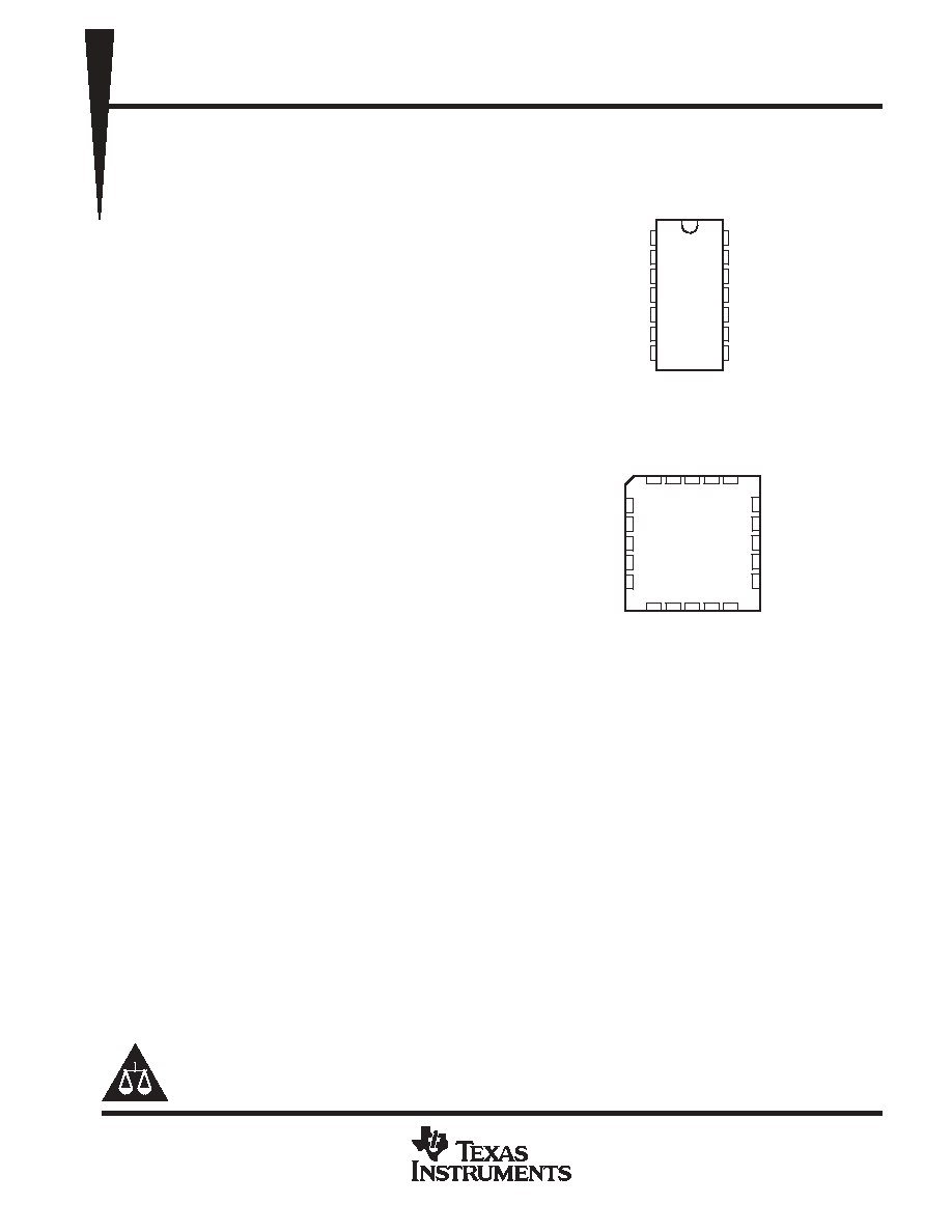
LM139, LM139A . . . D, J, OR W PACKAGE
LM239 . . . D, N, OR PW PACKAGE
LM239A . . . D PACKAGE
LM339, LM339A . . . D, DB, N, NS, OR PW PACKAGE
LM2901 . . . D, N, NS, OR PW PACKAGE
(TOP VIEW)
3
2 1 20 19
9 10 11 12 13
4
5
6
7
8
18
17
16
15
14
GND
NC
4IN+
NC
4IN-
V
CC
NC
2IN-
NC
2IN+
2OUT
1OUT
NC
3IN-
3IN+
3OUT
4OUT
1IN-
1IN+
NC
LM139, LM139A . . . FK PACKAGE
(TOP VIEW)
NC - No internal connection
On products compliant to MIL PRF 38535, all parameters are tested
unless otherwise noted. On all other products, production
processing does not necessarily include testing of all parameters.
LM139, LM139A, LM239, LM239A,
LM339, LM339A, LM2901, LM2901V
QUAD DIFFERENTIAL COMPARATORS
SLCS006L - OCTOBER 1979 - REVISED JUNE 2004
2
POST OFFICE BOX 655303
∑
DALLAS, TEXAS 75265
description/ordering information (continued)
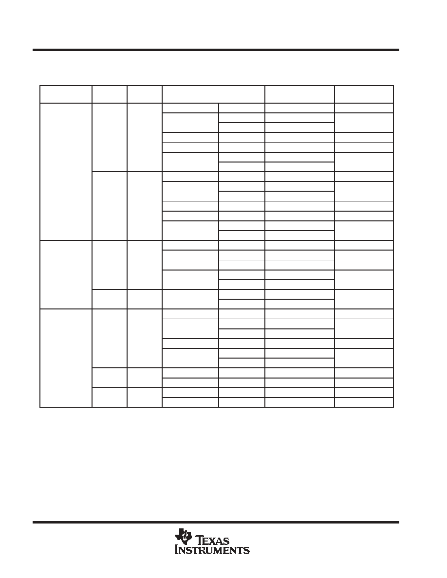
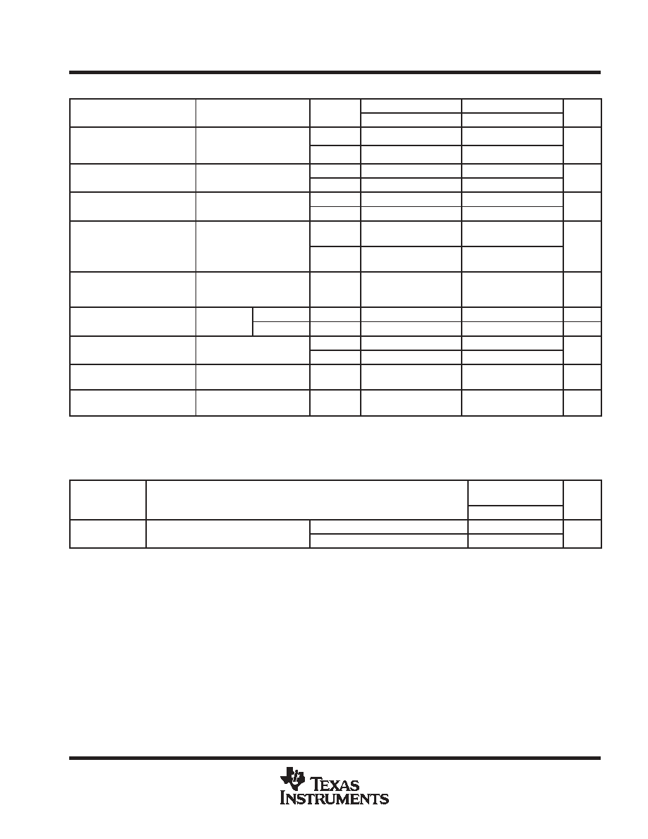
ORDERING INFORMATION
TA
VIOmax
AT 25
∞
C
MAX VCC
PACKAGE
ORDERABLE
PART NUMBER
TOP-SIDE
MARKING
PDIP (N)
Tube of 25
LM339N
LM339N
SOIC (D)
Tube of 50
LM339D
LM339
SOIC (D)
Reel of 2500
LM339DR
LM339
5 mV
30 V
SOP (NS)
Reel of 2000
LM339NSR
LM339
5 mV
30 V
SSOP (DB)
Reel of 2000
LM339DBR
LM339
TSSOP (PW)
Tube of 90
LM339PW
L339
0
∞
C to 70
∞
C
TSSOP (PW)
Reel of 2000
LM339PWR
L339
0
∞
C to 70
∞
C
PDIP (N)
Tube of 25
LM339AN
LM339AN
SOIC (D)
Tube of 50
LM339AD
LM339A
SOIC (D)
Reel of 2500
LM339ADR
LM339A
2 mV
30 V
SOP (NS)
Reel of 2000
LM339ANSR
LM339A
2 mV
30 V
SSOP (DB)
Reel of 2000
LM339ADBR
L339A
TSSOP (PW)
Tube of 90
LM339APW
L339A
TSSOP (PW)
Reel of 2000
LM339APWR
L339A
PDIP (N)
Tube of 25
LM239N
LM239N
SOIC (D)
Tube of 50
LM239D
LM239
5 mV
30 V
SOIC (D)
Reel of 2500
LM239DR
LM239
-25
∞
C to 85
∞
C
5 mV
30 V
TSSOP (PW)
Tube of 90
LM239PW
L239
-25 C to 85 C
TSSOP (PW)
Reel of 2000
LM239PWR
L239
2 mV
30 V
SOIC (D)
Tube of 50
LM239AD
LM239A
2 mV
30 V
SOIC (D)
Reel of 2500
LM239ADR
LM239A
PDIP (N)
Tube of 25
LM2901N
LM2901N
SOIC (D)
Tube of 50
LM2901D
LM2901
7 mV
30 V
SOIC (D)
Reel of 2500
LM2901DR
LM2901
7 mV
30 V
SOP (NS)
Reel of 2000
LM2901NSR
LM2901
-40
∞
C to 125
∞
C
TSSOP (PW)
Tube of 90
LM2901PW
L2901
-40
∞
C to 125
∞
C
TSSOP (PW)
Reel of 2000
LM2901PWR
L2901
7 mV
32 V
SOIC (D)
Reel of 2500
LM2901VQDR
L2901V
7 mV
32 V
TSSOP (PW)
Reel of 2000
LM2901VQPWR
L2901V
2 mV
32 V
SOIC (D)
Reel of 2500
LM2901AVQDR
L2901AV
2 mV
32 V
TSSOP (PW)
Reel of 2000
LM2901AVQPWR
L2901AV
Package drawings, standard packing quantities, thermal data, symbolization, and PCB design guidelines are available at
www.ti.com/sc/package.
LM139, LM139A, LM239, LM239A,
LM339, LM339A, LM2901, LM2901V
QUAD DIFFERENTIAL COMPARATORS
SLCS006L - OCTOBER 1979 - REVISED JUNE 2004
3
POST OFFICE BOX 655303
∑
DALLAS, TEXAS 75265
description/ordering information (continued)
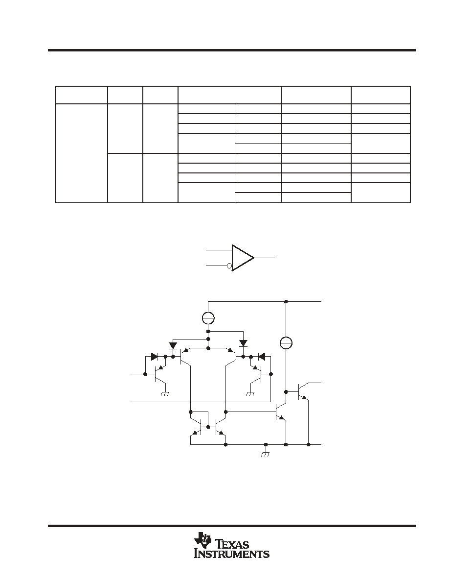
ORDERING INFORMATION
TA
VIOmax
AT 25
∞
C
MAX VCC
PACKAGE
ORDERABLE
PART NUMBER
TOP-SIDE
MARKING
CFP (W)
Tube of 25
LM139W
LM139W
CDIP (J)
Tube of 25
LM139J
LM139J
5 mV
30 V
LCCC (FK)
Tube of 55
LM139FK
LM139FK
5 mV
30 V
SOIC (D)
Tube of 50
LM139D
LM139D
- 55
∞
C to 125
∞
C
SOIC (D)
Reel of 2500
LM139DR
LM139D
- 55
∞
C to 125
∞
C
CFP (W)
Tube of 25
LM139AW
LM139AW
CDIP (J)
Tube of 25
LM139AJ
LM139AJ
2 mV
30 V
LCCC (FK)
Tube of 55
LM139AFK
LM139AFK
2 mV
30 V
SOIC (D)
Tube of 50
LM139AD
LM139AD
SOIC (D)
Reel of 2500
LM139ADR
LM139AD
Package drawings, standard packing quantities, thermal data, symbolization, and PCB design guidelines are available at
www.ti.com/sc/package.
symbol (each comparator)
OUT
IN-
IN+
schematic (each comparator)
80-
µ
A
Current
Regulator
80
µ
A
GND
OUT
VCC
10
µ
A
60
µ
A
10
µ
A
IN+
IN-
All current values shown are nominal.
LM139, LM139A, LM239, LM239A,
LM339, LM339A, LM2901, LM2901V
QUAD DIFFERENTIAL COMPARATORS
SLCS006L - OCTOBER 1979 - REVISED JUNE 2004
4
POST OFFICE BOX 655303
∑
DALLAS, TEXAS 75265
absolute maximum ratings over operating free-air temperature range (unless otherwise noted)
Supply voltage, V
CC
(see Note 1)
36 V
. . . . . . . . . . . . . . . . . . . . . . . . . . . . . . . . . . . . . . . . . . . . . . . . . . . . . . . . . . . .
Differential input voltage, V
ID
(see Note 2)
±
36 V
. . . . . . . . . . . . . . . . . . . . . . . . . . . . . . . . . . . . . . . . . . . . . . . . . . .
Input voltage range, V
I
(either input)
-0.3 V to 36 V
. . . . . . . . . . . . . . . . . . . . . . . . . . . . . . . . . . . . . . . . . . . . . . . . .
Output voltage, V
O
36 V
. . . . . . . . . . . . . . . . . . . . . . . . . . . . . . . . . . . . . . . . . . . . . . . . . . . . . . . . . . . . . . . . . . . . . . . . .
Output current, I
O
20 mA
. . . . . . . . . . . . . . . . . . . . . . . . . . . . . . . . . . . . . . . . . . . . . . . . . . . . . . . . . . . . . . . . . . . . . . . .
Duration of output short circuit to ground (see Note 3)
Unlimited
. . . . . . . . . . . . . . . . . . . . . . . . . . . . . . . . . . . . . .
Package thermal impedance,
JA
(see Notes 4 and 5): D package
86
∞
C/W
. . . . . . . . . . . . . . . . . . . . . . . . . . . .
DB package
96
∞
C/W
. . . . . . . . . . . . . . . . . . . . . . . . . . .
N package
80
∞
C/W
. . . . . . . . . . . . . . . . . . . . . . . . . . . .
NS package
76
∞
C/W
. . . . . . . . . . . . . . . . . . . . . . . . . . .
PW package
113
∞
C/W
. . . . . . . . . . . . . . . . . . . . . . . . .
Package thermal impedance,
JC
(see Notes 6 and 7): FK package
5.61
∞
C/W
. . . . . . . . . . . . . . . . . . . . . . . . .
J package
15.05
∞
C/W
. . . . . . . . . . . . . . . . . . . . . . . . .
W package
14.65
∞
C/W
. . . . . . . . . . . . . . . . . . . . . . . .
Operating virtual junction temperature, T
J
150
∞
C
. . . . . . . . . . . . . . . . . . . . . . . . . . . . . . . . . . . . . . . . . . . . . . . . . . .
Case temperature for 60 seconds: FK package
260
∞
C
. . . . . . . . . . . . . . . . . . . . . . . . . . . . . . . . . . . . . . . . . . . . . .
Lead temperature 1,6 mm (1/16 inch) from case for 60 seconds: J package
300
∞
C
. . . . . . . . . . . . . . . . . . . . .
Storage temperature range, T
stg
-65
∞
C to 150
∞
C
. . . . . . . . . . . . . . . . . . . . . . . . . . . . . . . . . . . . . . . . . . . . . . . . . . .
Stresses beyond those listed under "absolute maximum ratings" may cause permanent damage to the device. These are stress ratings only, and
functional operation of the device at these or any other conditions beyond those indicated under "recommended operating conditions" is not
implied. Exposure to absolute-maximum-rated conditions for extended periods may affect device reliability.
NOTES:
1. All voltage values, except differential voltages, are with respect to network ground.
2. Differential voltages are at IN+ with respect to IN-.
3. Short circuits from outputs to VCC can cause excessive heating and eventual destruction.
4. Maximum power dissipation is a function of TJ(max),
JA, and TA. The maximum allowable power dissipation at any allowable
ambient temperature is PD = (TJ(max) - TA)/
JA. Operating at the absolute maximum TJ of 150
∞
C can affect reliability.
5. The package thermal impedance is calculated in accordance with JESD 51-7.
6. Maximum power dissipation is a function of TJ(max),
JC, and TC. The maximum allowable power dissipation at any allowable case
temperature is PD = (TJ(max) - TC)/
JC. Operating at the absolute maximum TJ of 150
∞
C can affect reliability.
7. The package thermal impedance is calculated in accordance with MIL-STD-883.
LM139, LM139A, LM239, LM239A,
LM339, LM339A, LM2901, LM2901V
QUAD DIFFERENTIAL COMPARATORS
SLCS006L - OCTOBER 1979 - REVISED JUNE 2004
5
POST OFFICE BOX 655303
∑
DALLAS, TEXAS 75265
electrical characteristics at specified free-air temperature, V
CC
= 5 V (unless otherwise noted)
PARAMETER
TEST CONDITIONS
TA
LM139
LM139A
UNIT
PARAMETER
TEST CONDITIONS
TA
MIN
TYP
MAX
MIN
TYP
MAX
UNIT
VIO
Input offset voltage
VCC = 5 V to 30 V,
VIC = VICR(min),
25
∞
C
2
5
1
2
mV
VIO
Input offset voltage
VIC = VICR(min),
VO = 1.4 V
Full range
9
4
mV
IIO
Input offset current
VO = 1.4 V
25
∞
C
3
25
3
25
nA
IIO
Input offset current
VO = 1.4 V
Full range
100
100
nA
IIB
Input bias current
VO = 1.4 V
25
∞
C
-25
-100
-25
-100
nA
IIB
Input bias current
VO = 1.4 V
Full range
-300
-300
nA
VICR
Common-mode
25
∞
C
0 to
VCC-1.5
0 to
VCC-1.5
V
VICR
Common-mode
input-voltage range
Full range
0 to
VCC-2
0 to
VCC-2
V
AVD
Large-signal
differential-voltage
amplification
VCC
±
=
±
7.5 V,
VO = -5 V to 5 V
25
∞
C
200
50
200
V/mV
IOH
High-level output
VID = 1 V
VOH = 5 V
25
∞
C
0.1
0.1
nA
IOH
High-level output
current
VID = 1 V
VOH = 30 V
Full range
1
1
µ
A
VOL
Low-level output
VID = -1 V,
IOL = 4 mA
25
∞
C
150
400
150
400
mV
VOL
Low-level output
voltage
VID = -1 V,
IOL = 4 mA
Full range
700
700
mV
IOL
Low-level output
current
VID = -1 V,
VOL = 1.5 V
25
∞
C
6
16
6
16
mA
ICC
Supply current
(four comparators)
VO = 2.5 V,
No load
25
∞
C
0.8
2
0.8
2
mA
All characteristics are measured with zero common-mode input voltage, unless otherwise specified.
Full range (MIN to MAX) for LM139 and LM139A is -55
∞
C to 125
∞
C. All characteristics are measured with zero common-mode input voltage,
unless otherwise specified.
switching characteristics, V
CC
= 5 V, T
A
= 25
∞
C
PARAMETER
TEST CONDITIONS
LM139
LM139A
UNIT
PARAMETER
TEST CONDITIONS
MIN
TYP
MAX
UNIT
Response time
RL connected to 5 V through 5.1 k
,
ß
100-mV input step with 5-mV overdrive
1.3
µ
s
Response time
RL connected to 5 V through 5.1 k
,
CL = 15 pFß, See Note 8
TTL-level input step
0.3
µ
s
ß CL includes probe and jig capacitance.
NOTE 8: The response time specified is the interval between the input step function and the instant when the output crosses 1.4 V.