 | –≠–ª–µ–∫—Ç—Ä–æ–Ω–Ω—ã–π –∫–æ–º–ø–æ–Ω–µ–Ω—Ç: LM237KTE | –°–∫–∞—á–∞—Ç—å:  PDF PDF  ZIP ZIP |
LM237, LM337
3-TERMINAL ADJUSTABLE REGULATORS
SLVS047G ≠ NOVEMBER 1981 ≠ REVISED SEPTEMBER 2003
1
POST OFFICE BOX 655303
∑
DALLAS, TEXAS 75265
D
Output Voltage Range Adjustable From
≠1.2 V to ≠37 V
D
Output Current Capability of 1.5 A Max
D
Input Regulation Typically 0.01% Per
Input-Voltage Change
D
Output Regulation Typically 0.3%
D
Peak Output Current Constant Over
Temperature Range of Regulator
D
Ripple Rejection Typically 77 dB
D
Direct Replacement for Industry-Standard
LM237 and LM337
description/ordering information
The LM237 and LM337 are adjustable 3-terminal negative-voltage regulators capable of supplying in excess
of ≠1.5 A over an output voltage range of ≠1.2 V to ≠37 V. They are exceptionally easy to use, requiring only
two external resistors to set the output voltage and one output capacitor for frequency compensation. The
current design has been optimized for excellent regulation and low thermal transients. In addition, the LM237
and LM337 feature internal current limiting, thermal shutdown, and safe-area compensation, making them
virtually immune to failure by overloads.
The LM237 and LM337 serve a wide variety of applications, including local on-card regulation, programmable
output-voltage regulation, and precision current regulation.
ORDERING INFORMATION
TJ
PACKAGE
ORDERABLE
PART NUMBER
TOP-SIDE
MARKING
≠25
∞
C to 150
∞
C
TO-220 (KC)
Tube of 50
LM237KC
LM237
0 C to 125 C
PowerFLEX
(KTE)
Reel of 2000
LM337KTER
LM337
0
∞
C to 125
∞
C
PowerFLEX
(KTP)
Reel of 3000
LM337KTPR
L337
TO-220 (KC)
Tube of 50
LM337KC
LM337
Package drawings, standard packing quantities, thermal data, symbolization, and PCB design guidelines are available
at www.ti.com/sc/package.
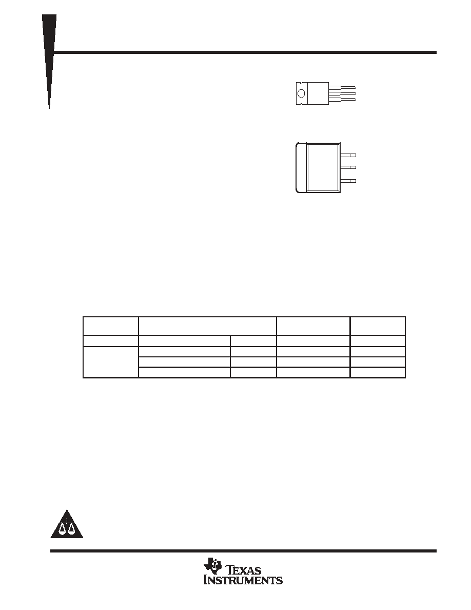
ADJUSTMENT
INPUT
OUTPUT
LM337 . . . KTE OR KTP PACKAGE
(TOP VIEW)
OUTPUT
ADJUSTMENT
INPUT
LM237, LM337 . . . KC (TO-220) PACKAGE
(TOP VIEW)
INPUT
INPUT
PRODUCTION DATA information is current as of publication date.
Products conform to specifications per the terms of Texas Instruments
standard warranty. Production processing does not necessarily include
testing of all parameters.
Copyright
2003, Texas Instruments Incorporated
Please be aware that an important notice concerning availability, standard warranty, and use in critical applications of
Texas Instruments semiconductor products and disclaimers thereto appears at the end of this data sheet.
PowerFLEX is a trademark of Texas Instruments.
LM237, LM337
3-TERMINAL ADJUSTABLE REGULATORS
SLVS047G ≠ NOVEMBER 1981 ≠ REVISED SEPTEMBER 2003
2
POST OFFICE BOX 655303
∑
DALLAS, TEXAS 75265
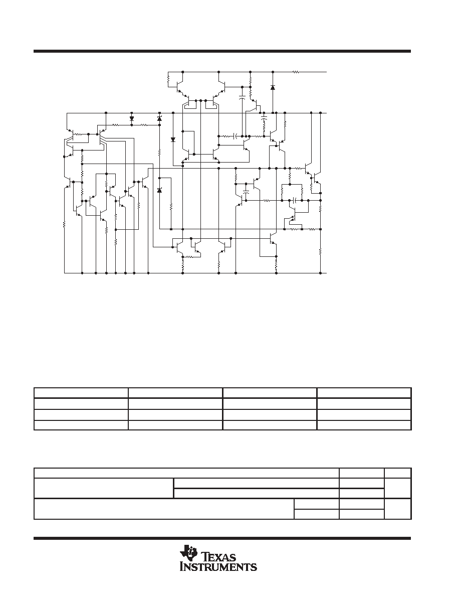
schematic diagram
ADJUSTMENT
OUTPUT
INPUT
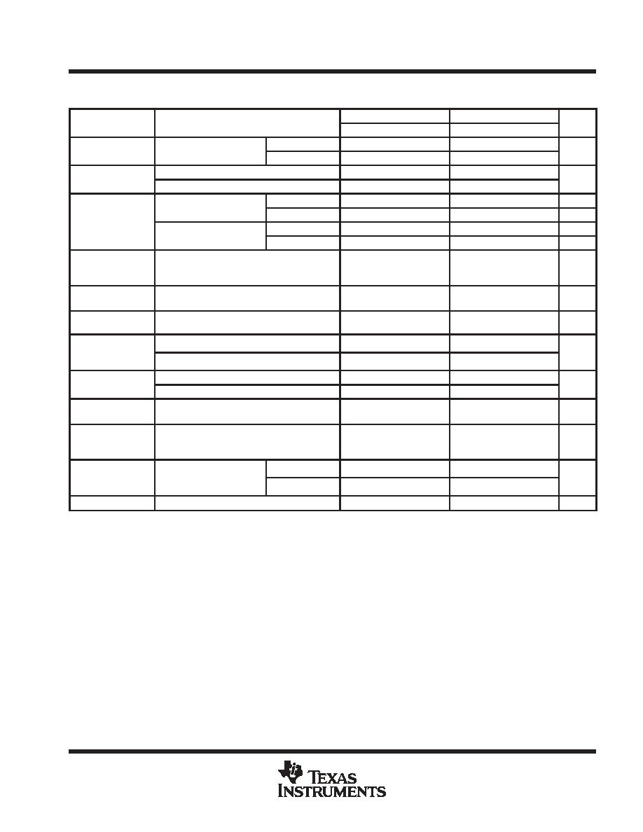
absolute maximum ratings over operating temperature ranges (unless otherwise noted)
Input-to-output differential voltage, V
I
≠ V
O
≠40
V
. . . . . . . . . . . . . . . . . . . . . . . . . . . . . . . . . . . . . . . . . . . . . . . . . . .
Operating virtual junction temperature, T
J
150
∞
C
. . . . . . . . . . . . . . . . . . . . . . . . . . . . . . . . . . . . . . . . . . . . . . . . . . .
Lead temperature 1,6 mm (1/16 inch) from case for 10 seconds
260
∞
C
. . . . . . . . . . . . . . . . . . . . . . . . . . . . . . .
Storage temperature range, T
stg
≠65
∞
C to 150
∞
C
. . . . . . . . . . . . . . . . . . . . . . . . . . . . . . . . . . . . . . . . . . . . . . . . . . .
Stresses beyond those listed under "absolute maximum ratings" may cause permanent damage to the device. These are stress ratings only, and
functional operation of the device at these or any other conditions beyond those indicated under "recommended operating conditions" is not
implied. Exposure to absolute-maximum-rated conditions for extended periods may affect device reliability.
package thermal data (see Note 1)
PACKAGE
BOARD
JC
JA
PowerFLEX
(KTE)
High K, JESD 51-5
3
∞
C/W
23
∞
C/W
PowerFLEX
(KTP)
High K, JESD 51-5
19
∞
C/W
28
∞
C/W
TO-220 (KC)
High K, JESD 51-5
3
∞
C/W
19
∞
C/W
NOTE 1: Maximum power dissipation is a function of TJ(max),
JA, and TA. The maximum allowable power dissipation at any allowable ambient
temperature is PD = (TJ(max) ≠ TA)/
JA. Operating at the absolute maximum TJ of 150
∞
C can affect reliability.
recommended operating conditions
MIN
MAX
UNIT
IO
Output current
|VI ≠ VO|
40 V,
P
15 W
10
1500
mA
IO
Output current
|VI ≠ VO|
10 V,
P
15 W
6
1500
mA
TJ
Operating virtual junction temperature
LM237
≠25
150
∞
C
TJ
Operating virtual junction temperature
LM337
0
125
∞
C
LM237, LM337
3-TERMINAL ADJUSTABLE REGULATORS
SLVS047G ≠ NOVEMBER 1981 ≠ REVISED SEPTEMBER 2003
3
POST OFFICE BOX 655303
∑
DALLAS, TEXAS 75265
electrical characteristics over recommended ranges of operating virtual junction temperature
(unless otherwise noted)
PARAMETER
TEST CONDITIONS
LM237
LM337
UNIT
PARAMETER
TEST CONDITIONS
MIN
TYP
MAX
MIN
TYP
MAX
UNIT
Input regulation
VI ≠ VO = ≠3 V to ≠40 V
TJ = 25
∞
C
0.01
0.02
0.01
0.04
%/V
Input regulation
VI ≠ VO = ≠3 V to ≠40 V
TJ = MIN to MAX
0.02
0.05
0.02
0.07
%/V
Ripple rejection
VO = ≠10 V,
f = 120 H
Z
60
60
dB
Ripple rejection
VO = ≠10 V, f = 120 H
Z,
CADJ = 10
µ
F
66
77
66
77
dB
Output regulation
IO = 10 mA to 1.5 A,
|VO|
5 V
25
50
mV
Output regulation
IO = 10 mA to 1.5 A,
TJ = 25
∞
C
|VO|
5 V
0.3%
0.5%
0.3%
1%
Output regulation
IO = 10 mA to 1.5 A
|VO|
5 V
50
70
mV
IO = 10 mA to 1.5 A
|VO|
5 V
1%
1.5%
Output-voltage
change with
temperature
TJ = MIN to MAX
0.6%
0.6%
Output-voltage
long-term drift
After 1000 h at TJ = MAX and VI ≠ VO = ≠40 V
0.3%
1%
0.3%
1%
Output noise
voltage
f = 10 H
Z
to 10 kH
Z
,
TJ = 25
∞
C
0.003%
0.003%
Minimum output
current to maintain
|VI ≠ VO|
40 V
2.5
5
2.5
10
mA
current to maintain
regulation
|VI ≠ VO|
10 V
1.2
3
1.5
6
mA
Peak output current
|VI ≠ VO|
15 V
1.5
2.2
1.5
2.2
A
Peak output current
|VI ≠ VO|
40 V,
TJ = 25
∞
C
0.24
0.4
0.15
0.4
A
Adjustment-terminal
current
65
100
65
100
µ
A
Change in
adjustment-terminal
current
VI ≠ VO = ≠ 2.5 V to ≠40 V,
IO = 10 mA to MAX
TJ = 25
∞
C,
2
5
2
5
µ
A
Reference voltage
VI ≠ VO = ≠ 3 V to ≠40 V,
IO = 10 mA to 1.5 A,
TJ = 25
∞
C
≠1.225
≠1.25
≠1.275
≠1.213
≠1.25
≠1.287
V
Reference voltage
(output to ADJ)
IO = 10 mA to 1.5 A,
P
rated dissipation
TJ = MIN to MAX
≠1.2
≠1.25
≠1.3
≠1.2
≠1.25
≠1.3
V
Thermal regulation
Initial TJ = 25
∞
C,
10-ms pulse
0.002
0.02
0.003
0.04
%/W
Unless otherwise noted, these specifications apply for the following test conditions |VI ≠ VO| = 5 V and IO = 0.5 A. For conditions shown as MIN
or MAX, use the appropriate value specified under recommended operating conditions. All characteristics are measured with a 0.1-
µ
F capacitor
across the input and a 1-
µ
F capacitor across the output. Pulse-testing techniques are used to maintain the junction temperature as close to the
ambient temperature as possible. Thermal effects must be taken into account separately.
Input regulation is expressed here as the percentage change in output voltage per 1-V change at the input.
LM237, LM337
3-TERMINAL ADJUSTABLE REGULATORS
SLVS047G ≠ NOVEMBER 1981 ≠ REVISED SEPTEMBER 2003
4
POST OFFICE BOX 655303
∑
DALLAS, TEXAS 75265
electrical characteristics, T
J
= 25
∞
C
PARAMETER
TEST CONDITIONS
LM237, LM337
UNIT
PARAMETER
TEST CONDITIONS
MIN
TYP
MAX
UNIT
Input regulation
VI ≠ VO = ≠3 V to ≠40 V
0.01
0.04
%/V
Ripple rejection
VO = ≠10 V,
f = 120 H
Z
60
dB
Ripple rejection
VO = ≠10 V, CADJ = 10
µ
F,
f = 120 H
Z
66
77
dB
Output regulation
IO = 10 mA to 1.5 A
|VO|
5 V
50
mV
Output regulation
IO = 10 mA to 1.5 A
|VO|
5 V
0.3%
1%
Output noise voltage
f = 10 H
Z
to 10 kH
Z
0.003%
Minimum output current to maintain regulation
|VI ≠ VO|
40 V
2.5
10
mA
Minimum output current to maintain regulation
|VI ≠ VO|
10 V
1.5
6
mA
Peak output current
|VI ≠ VO|
15 V
1.5
2.2
A
Peak output current
|VI ≠ VO|
40 V
0.15
0.4
A
Adjustment-terminal current
65
100
µ
A
Change in adjustment-terminal current
VI ≠ VO = ≠ 2.5 V to ≠40 V, IO = 10 mA to MAX
2
5
µ
A
Reference voltage (output to ADJ)
VI ≠ VO = ≠ 3 V to ≠40 V, IO = 10 mA to 1.5 A,
P
rated dissipation
≠1.213
≠1.25
≠1.287
V
Unless otherwise noted, these specifications apply for the following test conditions |VI ≠ VO| = 5 V and IO = 0.5 A. All characteristics are measured
with a 0.1-
µ
F capacitor across the input and a 1-
µ
F capacitor across the output. Pulse-testing techniques are used to maintain the junction
temperature as close to the ambient temperature as possible. Thermal effects must be taken into account separately.
Input regulation is expressed here as the percentage change in output voltage per 1-V change at the input.
LM237, LM337
3-TERMINAL ADJUSTABLE REGULATORS
SLVS047G ≠ NOVEMBER 1981 ≠ REVISED SEPTEMBER 2003
5
POST OFFICE BOX 655303
∑
DALLAS, TEXAS 75265
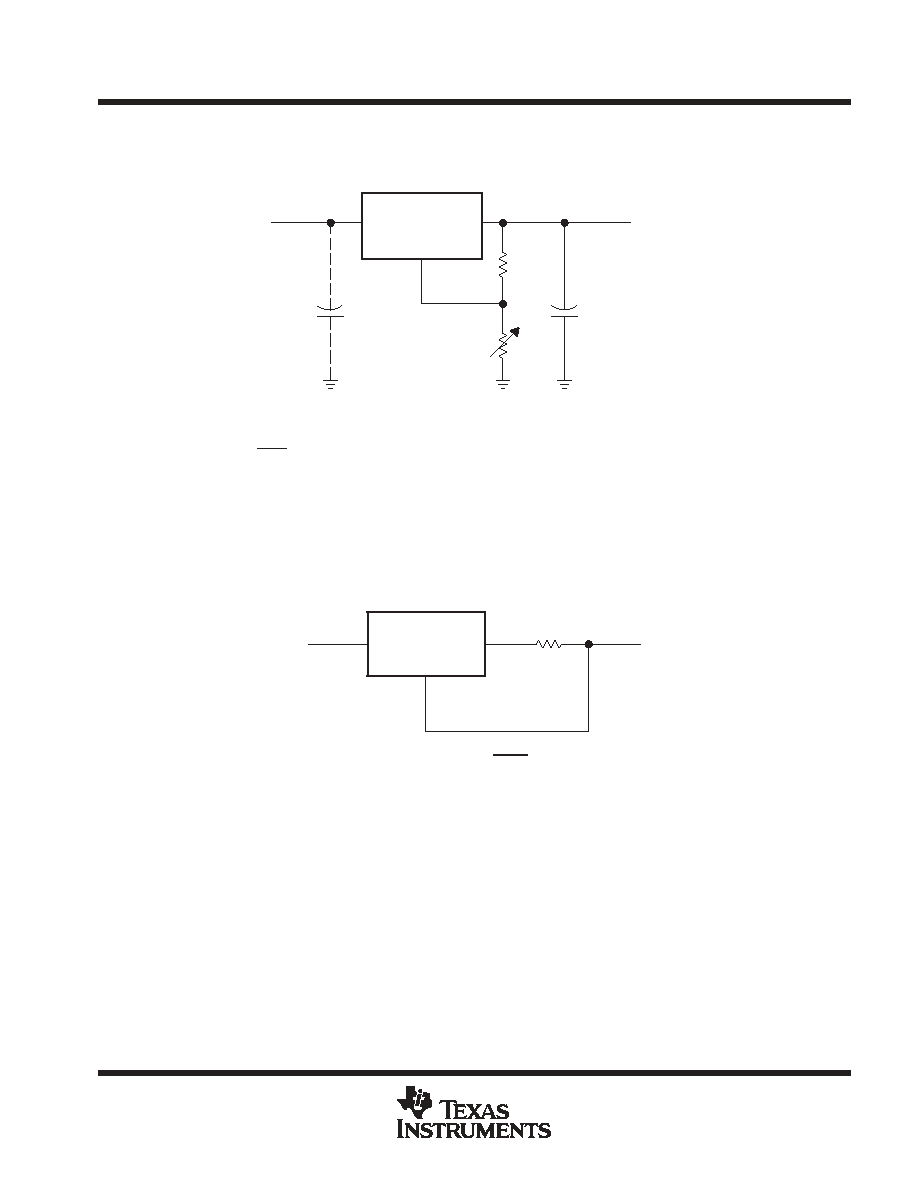
APPLICATION INFORMATION
C1
+
C2
R1
R2
+
INPUT
OUTPUT
ADJUSTMENT
LM237
or
LM337
VO
VI
C1 is a 1-
µ
F solid tantalum capacitor required only if the regulator is more than 10 cm (4 in) from the power-supply filter capacitor.
C2 is a 1-
µ
F solid tantalum or 10-
µ
F aluminum electrolytic capacitor required for stability.
R2
+
R1
≠V
O
≠1..25
*
1
R1 typically is 120
.
, where VO is the output in volts.
Figure 1. Adjustable Negative-Voltage Regulator
ADJUSTMENT
OUTPUT
INPUT
VI
RS
VO
LM237
or
LM337
RS =
1.25 V
ILIMIT
Figure 2. Current-Limiting Circuit