LM239A-Q1
QUAD DIFFERENTIAL COMPARATOR
SCLS513A ≠ JULY 2003 ≠ REVISED AUGUST 2003
1
POST OFFICE BOX 655303
∑
DALLAS, TEXAS 75265
D
Qualification in Accordance With
AEC-Q100
D
Qualified for Automotive Applications
D
Customer-Specific Configuration Control
Can Be Supported Along With
Major-Change Approval
D
ESD Protection Exceeds 1000 V Per
MIL-STD-883, Method 3015; Exceeds 100 V
Using Machine Model (C = 200 pF, R = 0);
Exceeds 2000 V Charged Device Model
D
Single Supply or Dual Supplies
D
Wide Range of Supply Voltage
. . . 2 V to 36 V
D
Low Supply-Current Drain Independent of
Supply Voltage . . . 0.8 mA Typ
D
Low Input Bias Current . . . 25 nA Typ
D
Low Input Offset Current . . . 5 nA Typ
Contact factory for details. Q100 qualification data available on
request.
D
Low Input Offset Voltage . . . 2 mV Typ
D
Common-Mode Input Voltage Range
Includes Ground
D
Differential Input Voltage Range Equal to
Maximum-Rated Supply Voltage . . .
±
36 V
D
Low Output Saturation Voltage
D
Output Compatible With TTL, MOS, and
CMOS
description/ordering information
This device consists of four independent voltage comparators that are designed to operate from a single power
supply over a wide range of voltages. Operation from dual supplies also is possible as long as the difference
between the two supplies is 2 V to 36 V, and V
CC
is at least 1.5 V more positive than the input common-mode
voltage. Current drain is independent of the supply voltage. The outputs can be connected to other
open-collector outputs to achieve wired-AND relationships.
ORDERING INFORMATION
TA
PACKAGE
ORDERABLE
PART NUMBER
TOP-SIDE
MARKING
≠40
∞
C to 125
∞
C
SOP ≠ D
Tape and reel
LM239AQDRQ1ß
LM239AQ1
Package drawings, standard packing quantities, thermal data, symbolization, and PCB
design guidelines are available at www.ti.com/sc/package.
ß This package is only available taped and reeled, with standard quantities of 2500 pieces per
reel.
symbol (each comparator)
OUT
IN≠
IN+
Please be aware that an important notice concerning availability, standard warranty, and use in critical applications of
Texas Instruments semiconductor products and disclaimers thereto appears at the end of this data sheet.
Copyright
2003, Texas Instruments Incorporated
PRODUCTION DATA information is current as of publication date.
Products conform to specifications per the terms of Texas Instruments
standard warranty. Production processing does not necessarily include
testing of all parameters.
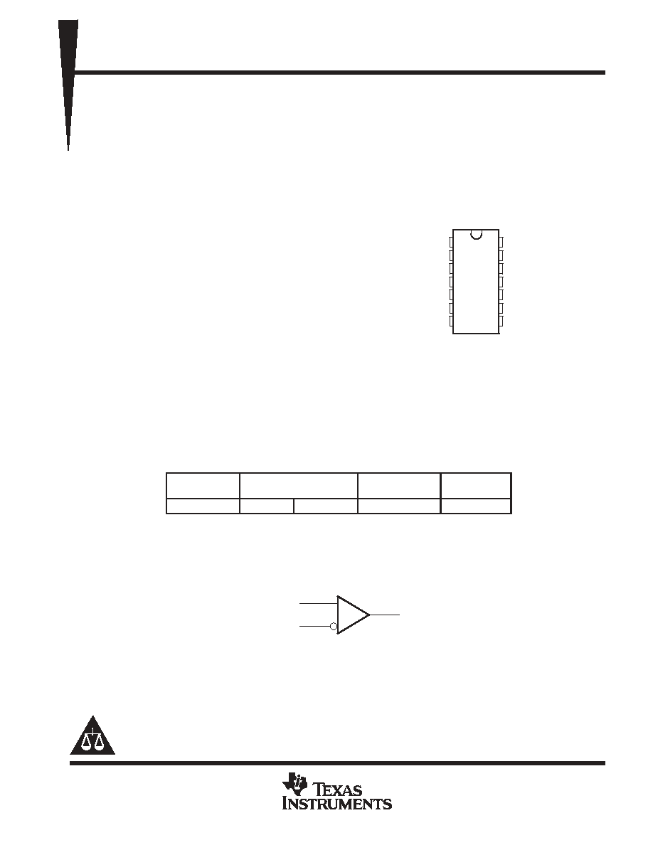
1
2
3
4
5
6
7
14
13
12
11
10
9
8
1OUT
2OUT
V
CC
2IN≠
2IN+
1IN≠
1IN+
OUT3
OUT4
GND
4IN+
4IN≠
3IN+
3IN≠
D PACKAGE
(TOP VIEW)
LM239A-Q1
QUAD DIFFERENTIAL COMPARATOR
SCLS513A ≠ JULY 2003 ≠ REVISED AUGUST 2003
2
POST OFFICE BOX 655303
∑
DALLAS, TEXAS 75265
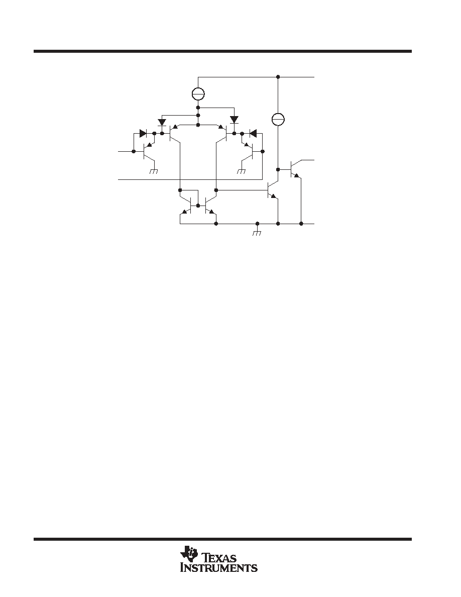
schematic (each comparator)
80-
µ
A
Current
Regulator
80
µ
A
GND
OUT
VCC
10
µ
A
60
µ
A
10
µ
A
IN+
IN≠
All current values shown are nominal.
absolute maximum ratings over operating free-air temperature range (unless otherwise noted)
Supply voltage, V
CC
(see Note 1)
36 V
. . . . . . . . . . . . . . . . . . . . . . . . . . . . . . . . . . . . . . . . . . . . . . . . . . . . . . . . . . . .
Differential input voltage, V
ID
(see Note 2)
±
36 V
. . . . . . . . . . . . . . . . . . . . . . . . . . . . . . . . . . . . . . . . . . . . . . . . . . .
Input voltage range, V
I
(either input)
≠0.3 V to 36 V
. . . . . . . . . . . . . . . . . . . . . . . . . . . . . . . . . . . . . . . . . . . . . . . . .
Output voltage, V
O
36 V
. . . . . . . . . . . . . . . . . . . . . . . . . . . . . . . . . . . . . . . . . . . . . . . . . . . . . . . . . . . . . . . . . . . . . . . . .
Output current, I
O
20 mA
. . . . . . . . . . . . . . . . . . . . . . . . . . . . . . . . . . . . . . . . . . . . . . . . . . . . . . . . . . . . . . . . . . . . . . . .
Duration of output short circuit to ground (see Note 3)
Unlimited
. . . . . . . . . . . . . . . . . . . . . . . . . . . . . . . . . . . . . .
Package thermal impedance,
JA
(see Note 4)
86
∞
C/W
. . . . . . . . . . . . . . . . . . . . . . . . . . . . . . . . . . . . . . . . . . . . .
Lead temperature 1,6 mm (1/16 inch) from case for 10 seconds
260
∞
C
. . . . . . . . . . . . . . . . . . . . . . . . . . . . . . .
Maximum operating junction temperature, T
J
136
∞
C
. . . . . . . . . . . . . . . . . . . . . . . . . . . . . . . . . . . . . . . . . . . . . . . .
Storage temperature range, T
stg
≠65
∞
C to 150
∞
C
. . . . . . . . . . . . . . . . . . . . . . . . . . . . . . . . . . . . . . . . . . . . . . . . . . .
Stresses beyond those listed under "absolute maximum ratings" may cause permanent damage to the device. These are stress ratings only, and
functional operation of the device at these or any other conditions beyond those indicated under "recommended operating conditions" is not
implied. Exposure to absolute-maximum-rated conditions for extended periods may affect device reliability.
NOTES:
1. All voltage values, except differential voltages, are with respect to network ground.
2. Differential voltages are at IN+ with respect to IN≠.
3. Short circuits from outputs to VCC can cause excessive heating and eventual destruction.
4. The package thermal impedance is calculated in accordance with JESD 51-7.
LM239A-Q1
QUAD DIFFERENTIAL COMPARATOR
SCLS513A ≠ JULY 2003 ≠ REVISED AUGUST 2003
3
POST OFFICE BOX 655303
∑
DALLAS, TEXAS 75265
electrical characteristics at specified free-air temperature, V
CC
= 5 V (unless otherwise noted)
PARAMETER
TEST CONDITIONS
TA
MIN
TYP
MAX
UNIT
VIO
Input offset voltage
VCC = 5 V to 30 V, VIC = VICR(min),
V = 1.4 V
25
∞
C
1
2.5
mV
VIO
Input offset voltage
CC
IC
ICR
VO = 1.4 V
Full range
5.5
mV
IIO
Input offset current
VO = 1.4 V
25
∞
C
5
50
nA
IIO
Input offset current
VO = 1.4 V
Full range
150
nA
IIB
Input bias current
VO = 1.4 V
25
∞
C
≠25
≠250
nA
IIB
Input bias current
VO = 1.4 V
Full range
≠400
nA
VICR
Common-mode input-voltage range
25
∞
C
0 to
VCC≠1.5
V
VICR
Common-mode input-voltage range
Full range
0 to
VCC≠2
V
AVD
Large-signal differential-voltage
amplification
VCC = 15 V, VO = 1.4 V to 11.4 V,
RL
15 k
to VCC
25
∞
C
50
200
V/mV
IOH
High-level output current
VID= 1 V
VOH = 5 V
25
∞
C
0.1
50
nA
IOH
High-level output current
VID= 1 V
VOH = 30 V
Full range
1
µ
A
VOL
Low-level output voltage
VID = ≠1 V,
IOL = 4 mA
25
∞
C
150
400
mV
VOL
Low-level output voltage
VID = ≠1 V,
IOL = 4 mA
Full range
700
mV
IOL
Low-level output current
VID = ≠1 V,
VOL = 1.5 V
25
∞
C
6
16
mA
ICC
Supply current (four comparators)
VO = 2.5 V,
No load
25
∞
C
0.8
2
mA
ICC
Supply current (four comparators)
VO = 2.5 V,
No load
25
∞
C
0.8
2
mA
All characteristics are measured with zero common-mode input voltage, unless otherwise specified.
Full range (MIN to MAX) for LM239AQ is ≠40
∞
C to 125
∞
C. All characteristics are measured with zero common-mode input voltage, unless
otherwise specified.
switching characteristics, V
CC
= 5 V, T
A
= 25
∞
C
PARAMETER
TEST CONDITIONS
MIN
TYP
MAX
UNIT
Response time
RL connected to 5 V through 5.1 k
,
C = 15 pFß, See Note 5
100-mV input step with 5-mV overdrive
1.3
µ
s
Response time
RL connected to 5 V through 5.1 k ,
CL = 15 pFß, See Note 5
TTL-level input step
0.3
µ
s
ß CL includes probe and jig capacitance.
NOTE 5: The response time specified is the interval between the input step function and the instant when the output crosses 1.4 V.
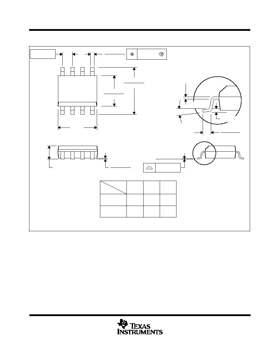
MECHANICAL DATA
MSOI002B ≠ JANUARY 1995 ≠ REVISED SEPTEMBER 2001
1
POST OFFICE BOX 655303
∑
DALLAS, TEXAS 75265
D (R-PDSO-G**)
PLASTIC SMALL-OUTLINE PACKAGE
8 PINS SHOWN
8
0.197
(5,00)
A MAX
A MIN
(4,80)
0.189
0.337
(8,55)
(8,75)
0.344
14
0.386
(9,80)
(10,00)
0.394
16
DIM
PINS **
4040047/E 09/01
0.069 (1,75) MAX
Seating Plane
0.004 (0,10)
0.010 (0,25)
0.010 (0,25)
0.016 (0,40)
0.044 (1,12)
0.244 (6,20)
0.228 (5,80)
0.020 (0,51)
0.014 (0,35)
1
4
8
5
0.150 (3,81)
0.157 (4,00)
0.008 (0,20) NOM
0
∞
≠ 8
∞
Gage Plane
A
0.004 (0,10)
0.010 (0,25)
0.050 (1,27)
NOTES: A. All linear dimensions are in inches (millimeters).
B. This drawing is subject to change without notice.
C. Body dimensions do not include mold flash or protrusion, not to exceed 0.006 (0,15).
D. Falls within JEDEC MS-012

IMPORTANT NOTICE
Texas Instruments Incorporated and its subsidiaries (TI) reserve the right to make corrections, modifications,
enhancements, improvements, and other changes to its products and services at any time and to discontinue
any product or service without notice. Customers should obtain the latest relevant information before placing
orders and should verify that such information is current and complete. All products are sold subject to TI's terms
and conditions of sale supplied at the time of order acknowledgment.
TI warrants performance of its hardware products to the specifications applicable at the time of sale in
accordance with TI's standard warranty. Testing and other quality control techniques are used to the extent TI
deems necessary to support this warranty. Except where mandated by government requirements, testing of all
parameters of each product is not necessarily performed.
TI assumes no liability for applications assistance or customer product design. Customers are responsible for
their products and applications using TI components. To minimize the risks associated with customer products
and applications, customers should provide adequate design and operating safeguards.
TI does not warrant or represent that any license, either express or implied, is granted under any TI patent right,
copyright, mask work right, or other TI intellectual property right relating to any combination, machine, or process
in which TI products or services are used. Information published by TI regarding third-party products or services
does not constitute a license from TI to use such products or services or a warranty or endorsement thereof.
Use of such information may require a license from a third party under the patents or other intellectual property
of the third party, or a license from TI under the patents or other intellectual property of TI.
Reproduction of information in TI data books or data sheets is permissible only if reproduction is without
alteration and is accompanied by all associated warranties, conditions, limitations, and notices. Reproduction
of this information with alteration is an unfair and deceptive business practice. TI is not responsible or liable for
such altered documentation.
Resale of TI products or services with statements different from or beyond the parameters stated by TI for that
product or service voids all express and any implied warranties for the associated TI product or service and
is an unfair and deceptive business practice. TI is not responsible or liable for any such statements.
Following are URLs where you can obtain information on other Texas Instruments products and application
solutions:
Products
Applications
Amplifiers
amplifier.ti.com
Audio
www.ti.com/audio
Data Converters
dataconverter.ti.com
Automotive
www.ti.com/automotive
DSP
dsp.ti.com
Broadband
www.ti.com/broadband
Interface
interface.ti.com
Digital Control
www.ti.com/digitalcontrol
Logic
logic.ti.com
Military
www.ti.com/military
Power Mgmt
power.ti.com
Optical Networking
www.ti.com/opticalnetwork
Microcontrollers
microcontroller.ti.com
Security
www.ti.com/security
Telephony
www.ti.com/telephony
Video & Imaging
www.ti.com/video
Wireless
www.ti.com/wireless
Mailing Address:
Texas Instruments
Post Office Box 655303 Dallas, Texas 75265
Copyright
2003, Texas Instruments Incorporated