 | –≠–ª–µ–∫—Ç—Ä–æ–Ω–Ω—ã–π –∫–æ–º–ø–æ–Ω–µ–Ω—Ç: LM2904-Q1 | –°–∫–∞—á–∞—Ç—å:  PDF PDF  ZIP ZIP |

LM2904 Q1
DUAL OPERATIONAL AMPLIFIER
SLOS414E - MAY 2003 - REVISED JUNE 2004
1
POST OFFICE BOX 655303
∑
DALLAS, TEXAS 75265
D
Qualification in Accordance With
AEC-Q100
D
Qualified for Automotive Applications
D
Customer-Specific Configuration Control
Can Be Supported Along With
Major-Change Approval
D
ESD Protection Exceeds 500 V Per
MIL-STD-883, Method 3015; Exceeds 200 V
Using Machine Model (C = 200 pF, R = 0)
D
Low Supply-Current Drain Independent of
Supply Voltage . . . 0.7 mA Typ
D
Common-Mode Input Voltage Range
Includes Ground, Allowing Direct Sensing
Near Ground
D
Differential Input Voltage Range Equal to
Maximum-Rated Supply Voltage:
- Non-V Devices . . .
±
26 V
- V-Suffix Devices . . .
±
32 V
Contact factory for details. Q100 qualification data available on
request.
D
Low Input Bias and Offset Parameters:
- Input Offset Voltage . . . 3 mV Typ
- Input Offset Current . . . 2 nA Typ
- Input Bias Current . . . 20 nA Typ
D
Open-Loop Differential Voltage
Amplification . . . 100 V/mV Typ
D
Internal Frequency Compensation
description/ordering information
This device consists of two independent, high-gain, frequency-compensated operational amplifiers designed
to operate from a single supply over a wide range of voltages. Operation from split supplies is possible as long
as the difference between the two supplies is 3 V to 26 V (3 V to 32 V for V-suffix devices), and V
CC
is at least
1.5 V more positive than the input common-mode voltage. The low supply-current drain is independent of the
magnitude of the supply voltage.
Applications include transducer amplifiers, dc amplification blocks, and all the conventional operational
amplifier circuits that now can be implemented more easily in single-supply-voltage systems. For example,
these devices can be operated directly from the standard 5-V supply used in digital systems and easily provide
the required interface electronics without additional
±
5-V supplies.
The LM2904Q is manufactured to demanding automotive requirements.
ORDERING INFORMATION
TA
VIOmax
AT 25
∞
C
MAX VCC
PACKAGE
ORDERABLE
PART NUMBER
TOP-SIDE
MARKING
7 mV
26 V
SOIC (D)
Tape and reel
LM2904QDRQ1
2904Q1
7 mV
26 V
TSSOP (PW)
Tape and reel
LM2904QPWRQ1
2904Q1
- 40
∞
C to 125
∞
C
7 mV
32 V
SOIC (D)
Tape and reel
LM2904VQDRQ1
2904VQ1
- 40
∞
C to 125
∞
C
7 mV
32 V
TSSOP (PW)
Tape and reel
LM2904VQPWRQ1
2904VQ1
2 mV
32 V
SOIC (D)
Tape and reel
LM2904AVQDRQ1
2904AVQ
2 mV
32 V
TSSOP (PW)
Tape and reel
LM2904AVQPWRQ1
2904AVQ
Package drawings, standard packing quantities, thermal data, symbolization, and PCB design guidelines are available at
www.ti.com/sc/package.
Please be aware that an important notice concerning availability, standard warranty, and use in critical applications of
Texas Instruments semiconductor products and disclaimers thereto appears at the end of this data sheet.
Copyright
2004, Texas Instruments Incorporated
PRODUCTION DATA information is current as of publication date.
Products conform to specifications per the terms of Texas Instruments
standard warranty. Production processing does not necessarily include
testing of all parameters.
1
2
3
4
8
7
6
5
1OUT
1IN-
1IN+
GND
V
CC
2OUT
2IN-
2IN+
D OR PW PACKAGE
(TOP VIEW)

LM2904 Q1
DUAL OPERATIONAL AMPLIFIER
SLOS414E - MAY 2003 - REVISED JUNE 2004
2
POST OFFICE BOX 655303
∑
DALLAS, TEXAS 75265
symbol (each amplifier)
IN+
IN-
OUT
+
-
schematic (each amplifier)
VCC+
OUT
GND (or VCC-)
To Other Amplifier
IN-
IN+
6-
µ
A
Current
Regulator
6-
µ
A
Current
Regulator
100-
µ
A
Current
Regulator
50-
µ
A
Current
Regulator
Epi-FET
Diodes
Resistors
Transistors
Capacitors
COMPONENT COUNT
1
2
7
51
2
LM2904 Q1
DUAL OPERATIONAL AMPLIFIER
SLOS414E - MAY 2003 - REVISED JUNE 2004
3
POST OFFICE BOX 655303
∑
DALLAS, TEXAS 75265
absolute maximum ratings over operating free-air temperature (unless otherwise noted)
Supply voltage, V
CC
(see Note 1): Non-V devices
26 V
. . . . . . . . . . . . . . . . . . . . . . . . . . . . . . . . . . . . . . . . . . . . .
V-suffix devices
32 V
. . . . . . . . . . . . . . . . . . . . . . . . . . . . . . . . . . . . . . . . . . . . .
Differential input voltage, V
ID
(see Note 2): Non-V devices
±
26 V
. . . . . . . . . . . . . . . . . . . . . . . . . . . . . . . . . . . . .
V-suffix devices
±
32 V
. . . . . . . . . . . . . . . . . . . . . . . . . . . . . . . . . . . .
Input voltage range, V
I
(either input): Non-V devices
-0.3 V to 26 V
. . . . . . . . . . . . . . . . . . . . . . . . . . . . . . . . . .
V-suffix devices
-0.3 V to 32 V
. . . . . . . . . . . . . . . . . . . . . . . . . . . . . . . . .
Duration of output short circuit (one amplifier) to ground at (or below) 25
∞
C
free-air temperature (V
CC
15 V) (see Note 3)
Unlimited
. . . . . . . . . . . . . . . . . . . . . . . . . . . . . . . . . . . . . . . . . .
Operating virtual junction temperature, T
J
150
∞
C
. . . . . . . . . . . . . . . . . . . . . . . . . . . . . . . . . . . . . . . . . . . . . . . . . . .
Package thermal impedance,
JA
(see Notes 4 and 5): D package
97
∞
C/W
. . . . . . . . . . . . . . . . . . . . . . . . . . . . .
PW package
149
∞
C/W
. . . . . . . . . . . . . . . . . . . . . . . . . .
Operating free-air temperature range, T
A
-40
∞
C to 125
∞
C
. . . . . . . . . . . . . . . . . . . . . . . . . . . . . . . . . . . . . . . . . . .
Storage temperature range, T
stg
-65
∞
C to 150
∞
C
. . . . . . . . . . . . . . . . . . . . . . . . . . . . . . . . . . . . . . . . . . . . . . . . . . .
Stresses beyond those listed under "absolute maximum ratings" may cause permanent damage to the device. These are stress ratings only, and
functional operation of the device at these or any other conditions beyond those indicated under "recommended operating conditions" is not
implied. Exposure to absolute-maximum-rated conditions for extended periods may affect device reliability.
NOTES:
1. All voltage values, except differential voltages and VCC specified for measurement of IOS, are with respect to the network ground
terminal.
2. Differential voltages are at IN+ with respect to IN-.
3. Short circuits from outputs to VCC can cause excessive heating and eventual destruction.
4. Maximum power dissipation is a function of TJ(max),
JA, and TA. The maximum allowable power dissipation at any allowable
ambient temperature is PD = (TJ(max) - TA)/
JA. Operating at the absolute maximum TJ of 150
∞
C can affect reliability.
5. The package thermal impedance is calculated in accordance with JESD 51-7.
LM2904 Q1
DUAL OPERATIONAL AMPLIFIER
SLOS414E - MAY 2003 - REVISED JUNE 2004
4
POST OFFICE BOX 655303
∑
DALLAS, TEXAS 75265
electrical characteristics at specified free-air temperature, V
CC
= 5 V (unless otherwise noted)
PARAMETER
TEST CONDITIONS
TA
MIN
TYPß
MAX
UNIT
VCC = 5 V to
Non-A devices
25
∞
C
3
7
VIO
Input offset voltage
VCC = 5 V to
MAX,
Non-A devices
Full range
10
mV
VIO
Input offset voltage
MAX,
VIC = VICR(min),
VO = 1.4 V
A-suffix devices
25
∞
C
1
2
mV
VIC = VICR(min),
VO = 1.4 V
A-suffix devices
Full range
4
a
V
IO
Average temperature coefficient of
input offset voltage
Full range
7
µ
V/
∞
C
Non-V devices
25
∞
C
2
50
IIO
Input offset current
VO = 1.4 V
Non-V devices
Full range
300
nA
IIO
Input offset current
VO = 1.4 V
V-suffix devices
25
∞
C
5
50
nA
V-suffix devices
Full range
150
a
I
IO
Average temperature coefficient of
input offset current
Full range
10
pA/
∞
C
IIB
Input bias current
VO = 1.4 V
25
∞
C
-20
-250
nA
IIB
Input bias current
VO = 1.4 V
Full range
-500
nA
IB
Drift
Full range
50
pA/
∞
C
VICR
Common-mode input voltage range
VCC = 5 V to MAX
25
∞
C
0 to
VCC-1.5
V
VICR
Common-mode input voltage range
VCC = 5 V to MAX
Full range
0 to
VCC-2
V
RL
10 k
25
∞
C
VCC-1.5
VCC = MAX,
RL = 2 k
Full range
22
VOH
High-level output voltage
VCC = MAX,
Non-V devices
RL
10 k
Full range
23
24
V
VOH
High-level output voltage
VCC = MAX,
RL = 2 k
Full range
26
V
VCC = MAX,
V-suffix devices
RL
10 k
Full range
27
28
VOL
Low-level output voltage
RL
10 k
Full range
5
20
mV
AVD
Large-signal differential
VCC = 15 V, VO = 1 V to 11 V,
25
∞
C
25
100
V/mV
AVD
Large-signal differential
voltage amplification
VCC = 15 V, VO = 1 V to 11 V,
RL =
2 k
Full range
15
V/mV
CMRR
Common-mode rejection ratio
VCC = 5 V to MAX,
VIC = VICR(min)
25
∞
C
65
80
dB
kSVR
Supply-voltage rejection ratio
(
VDD/
VIO)
VCC = 5 V to MAX
25
∞
C
65
100
dB
VO1/VO2
Crosstalk attenuation
f = 1 kHz to 20 kHz
25
∞
C
120
dB
VCC = 15 V, VID = 1 V, VO = 0
25
∞
C
-20
-30
VCC = 15 V, VID = 1 V, VO = 0
Full range
-10
mA
IO
Output current
VCC = 15 V, VID = -1 V, VO = 15 V
25
∞
C
10
20
mA
IO
Output current
VCC = 15 V, VID = -1 V, VO = 15 V
Full range
5
VID = -1 V,
VO = 200 mV
25
∞
C
12
40
µ
A
IOS
Short-circuit output current
VCC at 5 V, GND at -5 V, VO = 0
25
∞
C
±
40
±
60
mA
ICC
Supply current (two amplifiers)
VO = 2.5 V,
No load
Full range
0.7
1.2
mA
ICC
Supply current (two amplifiers)
VCC = MAX, VO = 0.5 VCC, No load
Full range
1
2
mA
All characteristics are measured under open-loop conditions, with zero common-mode input voltage, unless otherwise specified. MAX VCC for
testing purposes is 26 V for non-V devices and 32 V for V-suffix devices.
Full range is -40
∞
C to 125
∞
C for LM2904Q.S
ß All typical values are at TA = 25
∞
C.
LM2904 Q1
DUAL OPERATIONAL AMPLIFIER
SLOS414E - MAY 2003 - REVISED JUNE 2004
5
POST OFFICE BOX 655303
∑
DALLAS, TEXAS 75265
operating conditions, V
CC
=
±
15 V, T
A
= 25
∞
C
PARAMETER
TEST CONDITIONS
TYP
UNIT
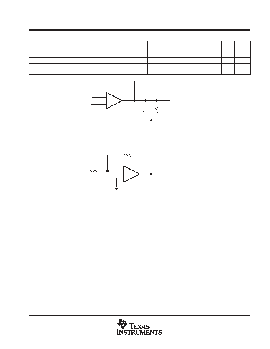
SR
Slew rate at unity gain
RL = 1 M
, CL = 30 pF, VI =
±
10 V
(see Figure 1)
0.3
V/
µ
s
B1
Unity-gain bandwidth
RL = 1 M
, CL = 20 pF (see Figure 1)
0.7
MHz
Vn
Equivalent input noise voltage
RS = 100
, VI = 0 V, f = 1 kHz
(see Figure 2)
40
nV/
Hz
CL
VO
VI
-
+
RL
VCC+
VCC-
Figure 1. Unity-Gain Amplifier
VO
-
+
100
VCC+
VCC-
RS
900
VI = 0 V
Figure 2. Noise-Test Circuit