 | –≠–ª–µ–∫—Ç—Ä–æ–Ω–Ω—ã–π –∫–æ–º–ø–æ–Ω–µ–Ω—Ç: LM306P | –°–∫–∞—á–∞—Ç—å:  PDF PDF  ZIP ZIP |
LM306
DIFFERENTIAL COMPARATOR WITH STROBES
SLCS008A ≠ OCTOBER 1979 ≠ REVISED OCTOBER 1991
1
POST OFFICE BOX 655303
∑
DALLAS, TEXAS 75265
D
Fast Response Times
D
Improved Gain and Accuracy
D
Fanout to 10 Series 54/74 TTL Loads
D
Strobe Capability
D
Short-Circuit and Surge Protection
D
Designed to Be Interchangeable With
National Semiconductor LM306
description
The LM306 is a high-speed voltage comparator
with differential inputs, a low-impedance high-
sink-current (100 mA) output, and two strobe
inputs. This device detects low-level analog or
digital signals and can drive digital logic or lamps
and relays directly. Short-circuit protection and
surge-current limiting is provided.
A low-level input at either strobe causes the output
to remain high regardless of the differential
input.When both strobe inputs are either open or
at a high logic level, the output voltage is
controlled by the differential input voltage. The
circuit will operate with any negative supply
voltage between ≠ 3 V and ≠ 12 V with little
difference in performance.
The LM306 is characterized for operation from
0
∞
C to 70
∞
C.
AVAILABLE OPTIONS
VIOmax
PACKAGE
TA
VIOmax
at 25
∞
C
SMALL OUTLINE
PLASTIC DIP
at 25 C
(D)
(P)
0
∞
C to 70
∞
C
5 mV
LM306D
LM306P
Copyright
©
1991, Texas Instruments Incorporated
PRODUCTION DATA information is current as of publication date.
Products conform to specifications per the terms of Texas Instruments
standard warranty. Production processing does not necessarily include
testing of all parameters.
1
2
3
4
8
7
6
5
GND
IN +
IN ≠
V
CC ≠
V
CC+
OUT
STROBE 2
STROBE 1
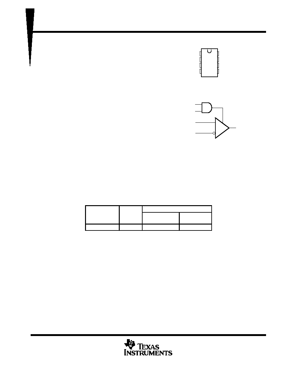
D OR P PACKAGE
(TOP
VIEW)
IN ≠
IN+
STROBE 2
STROBE 1
OUT
functional block diagram
LM306
DIFFERENTIAL COMPARATOR WITH STROBES
SLCS008A ≠ OCTOBER 1979 ≠ REVISED OCTOBER 1991
2
POST OFFICE BOX 655303
∑
DALLAS, TEXAS 75265
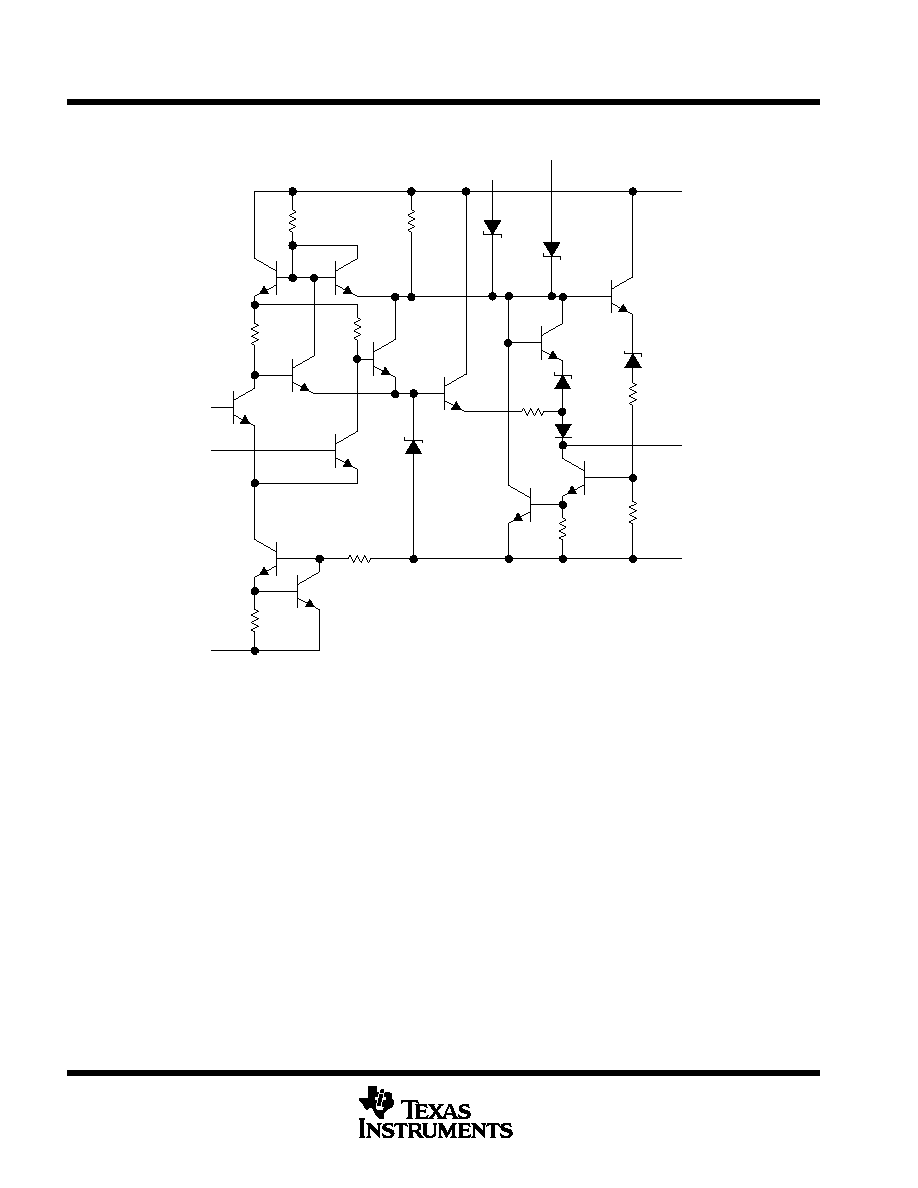
schematic
VCC ≠
IN ≠
IN +
70
STROBE 2
STROBE 1
VCC +
OUT
GND
6.3 V
6.3 V
6.3 V
6.3 V
5 k
6.3 V
17 k
300
5 k
300
600
3.5 k
600
3
Resistor values are nominal.
LM306
DIFFERENTIAL COMPARATOR WITH STROBES
SLCS008A ≠ OCTOBER 1979 ≠ REVISED OCTOBER 1991
3
POST OFFICE BOX 655303
∑
DALLAS, TEXAS 75265
absolute maximum ratings over operating free-air temperature range (unless otherwise noted)
Supply voltage, V
CC +
(see Note 1)
15 V
. . . . . . . . . . . . . . . . . . . . . . . . . . . . . . . . . . . . . . . . . . . . . . . . . . . . . . . . . . .
Supply voltage, V
CC ≠
(see Note 1)
≠ 15 V
. . . . . . . . . . . . . . . . . . . . . . . . . . . . . . . . . . . . . . . . . . . . . . . . . . . . . . . . . .
Differential input voltage, V
ID
(see Note 2)
±
5 V
. . . . . . . . . . . . . . . . . . . . . . . . . . . . . . . . . . . . . . . . . . . . . . . . . . . .
Input voltage, V
I
(either input, see Notes 1 and 3)
±
7 V
. . . . . . . . . . . . . . . . . . . . . . . . . . . . . . . . . . . . . . . . . . . . . .
Strobe voltage range (see Note 1)
0 V to V
CC+
. . . . . . . . . . . . . . . . . . . . . . . . . . . . . . . . . . . . . . . . . . . . . . . . . . . .
Output voltage, V
O
(see Note 1)
24 V
. . . . . . . . . . . . . . . . . . . . . . . . . . . . . . . . . . . . . . . . . . . . . . . . . . . . . . . . . . . . .
Voltage from output to V
CC ≠
30 V
. . . . . . . . . . . . . . . . . . . . . . . . . . . . . . . . . . . . . . . . . . . . . . . . . . . . . . . . . . . . . . . .
Duration of output short circuit to ground (see Note 4)
10 s
. . . . . . . . . . . . . . . . . . . . . . . . . . . . . . . . . . . . . . . . . .
Continuous total dissipation
See Dissipation Rating Table
. . . . . . . . . . . . . . . . . . . . . . . . . . . . . . . . . . . . . . . . . . .
Operating free-air temperature range, T
A
0
∞
C to 70
∞
C
. . . . . . . . . . . . . . . . . . . . . . . . . . . . . . . . . . . . . . . . . . . . . .
Storage temperature range
≠ 65
∞
C to 150
∞
C
. . . . . . . . . . . . . . . . . . . . . . . . . . . . . . . . . . . . . . . . . . . . . . . . . . . . . . . .
Lead temperature 1,6 mm (1/16 inch) from case for 10 seconds
260
∞
C
. . . . . . . . . . . . . . . . . . . . . . . . . . . . . . .
Stresses beyond those listed under "absolute maximum ratings" may cause permanent damage to the device. These are stress ratings only, and
functional operation of the device at these or any other conditions beyond those indicated under "recommended operating conditions" is not
implied. Exposure to absolute-maximum-rated conditions for extended periods may affect device reliability.
NOTES:
1. All voltage values, except differential voltages and the voltage from the output to VCC ≠, are with respect to the network ground.
2. Differential voltages are at IN+ with respect to IN ≠.
3. The magnitude of the input voltage must never exceed the magnitude of the supply voltage or 7 V, whichever is less.
4. The output may be shorted to ground or either power supply.
DISSIPATION RATING TABLE
PACKAGE
TA
25
∞
C
POWER RATING
DERATING
FACTOR
DERATE
ABOVE TA
TA = 70
∞
C
POWER RATING
D
P
600 mW
600 mW
5.8 mW/
∞
C
8.0 mW/
∞
C
46
∞
C
75
∞
C
464 mW
600 mW
LM306
DIFFERENTIAL COMPARATOR WITH STROBES
SLCS008A ≠ OCTOBER 1979 ≠ REVISED OCTOBER 1991
4
POST OFFICE BOX 655303
∑
DALLAS, TEXAS 75265
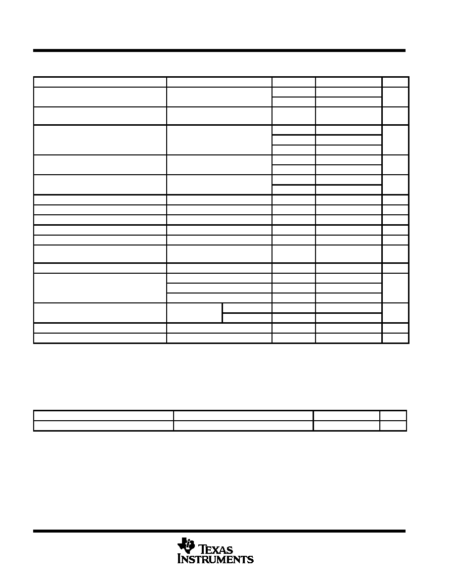
electrical characteristics at specified free-air temperature, V
CC+
= 12 V, V
CC ≠
= ≠3 V to ≠12 V (unless
otherwise noted)
PARAMETER
TEST CONDITIONS
TA
MIN
TYP
MAX
UNIT
VIO
Input offset voltage
RS
200
25
∞
C
1.6ß
5
mV
VIO
Input offset voltage
RS
200
Full range
6.5
mV
VIO
Average temperature coefficient of
input offset voltage
RS = 50
,
See Note 5
Full range
5
20
µ
V/
∞
C
25
∞
C
1.8
5
IIO
Input offset current
See Note 5
MIN
1
7.5
µ
A
MAX
0.5
5
IIO
Average temperature coefficient of
See Note 5
MIN to 25
∞
C
24
100
nA /
∞
C
IIO
g
input offset current
See Note 5
25
∞
C to MAX
15
50
nA /
∞
C
IIB
Input bias current
VO = 0 5 V to 5 V
MIN to 25
∞
C
40
µ
A
IIB
Input bias current
VO = 0.5 V to 5 V
25
∞
C to MAX
16
25
µ
A
IIL(S)
Low-level strobe current
V(strobe) = 0.4 V
Full range
≠ 1.7
≠ 3.2
mA
VIH(S)
High-level strobe voltage
Full range
2.2
V
VIL(S)
Low-level strobe voltage
Full range
0.9
V
VICR
Common-mode input voltage range
VCC ≠ = ≠ 7 V to ≠ 12 V
Full range
±
5
V
VID
Differential input voltage range
Full range
±
5
V
AVD
Large-signal differential voltage
amplification
VO = 0.5 V to 5 V,
No load
25
∞
C
40
V/mV
VOH
High-level output voltage
IOH = ≠ 400
µ
A
VID = 8 mV
Full range
2.5
5.5
V
IOL = 100 mA
VID = ≠ 7 mV
25
∞
C
0.8
2
VOL
Low-level output voltage
IOL = 50 mA
VID = ≠ 7 mV
Full range
1
V
IOL = 16 mA
VID = ≠ 8 mV
Full range
0.4
IOH
High level output voltage
VOH = 8 V to 24 V
VD = 7 mV
MIN to 25
∞
C
0.02
2
µ
A
IOH
High-level output voltage
VOH = 8 V to 24 V
VID = 8 mV
25
∞
C to MAX
100
µ
A
ICC +
Supply current from VCC +
VID = ≠ 5 mV,
No load
Full range
6.6
10
mA
ICC ≠
Supply current from VCC ≠
No load
Full range
≠ 1.9
≠ 3.6
mA
Unless otherwise noted, all characteristics are measured with both strobes open.
Full range is 0
∞
C to 70
∞
C. MIN is 0
∞
C. MAX is 70
∞
C.
ß This typical value is at VCC+ = 12 V, VCC≠ = ≠6 V.
NOTE 5: The offset voltages and offset currents given are the maximum values required to drive the output down to the low range (VOL) or up
to the high range (VOH). These parameters actually define an error band and take into account the worst-case effects of voltage gain
and input impedance.
switching characteristics, V
CC +
= 12 V, V
CC ≠
= ≠ 6 V, T
A
= 25
∞
C
PARAMETER
TEST CONDITIONS
MIN
TYP
MAX
UNIT
Response time, low-to-high-level output
RL = 390
to 5 V,
CL = 15 pF,
See Note 6
28
40
ns
All characteristics are measured with both strobes open.
NOTE 6: The response time specified is for a 100-mV input step with 5-mV overdrive and is the interval between the input step function and the
instant when the output crosses 1.4 V.
LM306
DIFFERENTIAL COMPARATOR WITH STROBES
SLCS008A ≠ OCTOBER 1979 ≠ REVISED OCTOBER 1991
5
POST OFFICE BOX 655303
∑
DALLAS, TEXAS 75265
TYPICAL CHARACTERISTICS
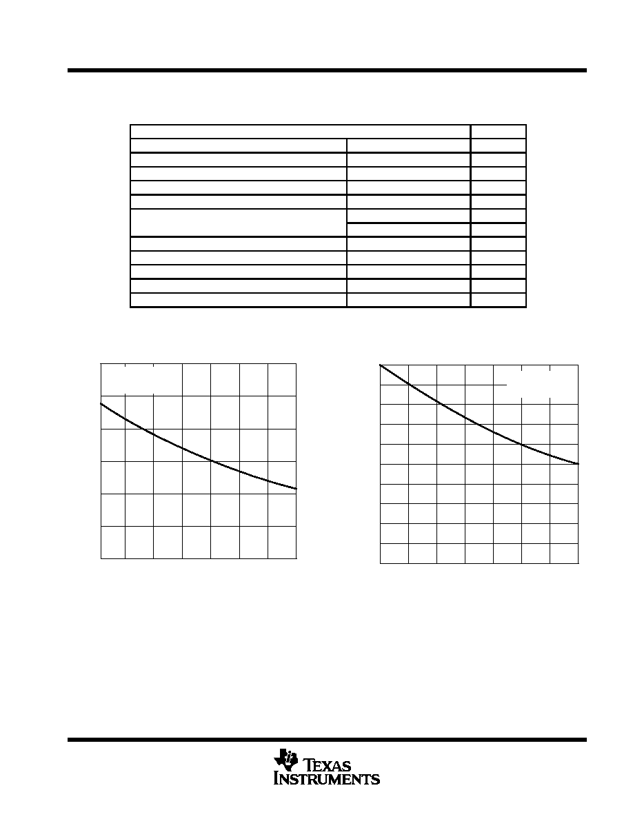
Table of Graphs
FIGURE
IIB
Input bias current
vs Free-air temperature
1
IIO
Input offset current
vs Free-air temperature
2
VOH
High-level output voltage
vs Free-air temperature
3
VOL
Low-level output voltage
vs Free-air temperature
4
VO
Output voltage
vs Differential input voltage
5
IO
Output current
vs Differential input voltage
6
AVD
Large-signal differential voltage amplification
vs Free-air temperature
7
IOS
Short-circuit output current
vs Free-air temperature
8
Output response
vs Time
9, 10
ICC+
Positive supply current
vs Positive supply voltage
11
ICC≠
Negative supply current
vs Negative supply voltage
12
PD
Total power dissipation
vs Free-air temperature
13
Figure 1
1.5
1
0.5
0
0
10
20
30
40
50
2
2.5
INPUT OFFSET CURRENT
vs
FREE-AIR TEMPERATURE
3
60
70
VCC+ = 12 V
VCC ≠ = ≠ 6 V
VO = 0.5 V to 5 V
TA ≠ Free Air Temperature ≠
∞
C
I IO
≠ Input Offset Current ≠
A
µ
Figure 2
10
8
2
0
0
10
20
30
40
50
60
≠ Input Bias Current ≠
14
18
INPUT BIAS CURRENT
vs
FREE-AIR TEMPERATURE
20
70
6
16
12
4
VCC+ = 12 V
VCC ≠ = ≠ 6 V
VO = 0.5 V to 5 V
TA ≠ Free-Air Temperature ≠
∞
C
I IB
A
µ