www.ti.com
FEATURES
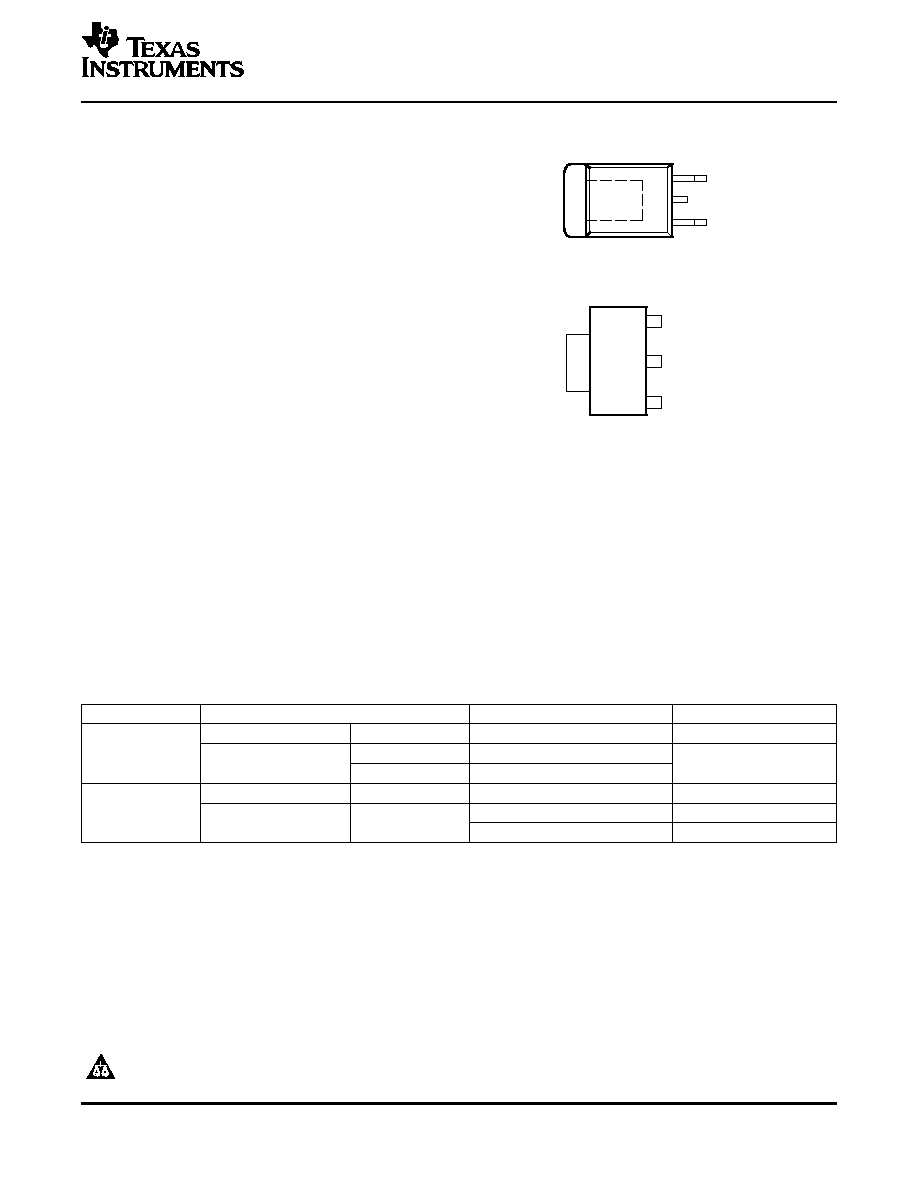
KTP PACKAGE
(TOP VIEW)
INPUT
ADJUST
DCY PACKAGE
(TOP VIEW)
INPUT
OUTPUT
ADJUST
OUTPUT
OUTPUT
DESCRIPTION/ORDERING INFORMATION
LM317M
3-TERMINAL ADJUSTABLE REGULATOR
SLVS297M ≠ APRIL 2000 ≠ REVISED OCTOBER 2005
∑
Output Voltage Range Adjustable From 1.25 V
to 37 V
∑
Output Current Greater Than 500 mA
∑
Internal Short-Circuit Current Limiting
∑
Thermal-Overload Protection
∑
Output Safe-Area Compensation
∑
Q Devices Meet Automotive Performance
Requirements
∑
Customer-Specific Configuration Control Can
Be Supported for Q Devices Along With
Major-Change Approval
The LM317M is an adjustable 3-terminal positive-voltage regulator capable of supplying more than 500 mA over
an output-voltage range of 1.25 V to 37 V. The LM317M is exceptionally easy to use and requires only two
external resistors to set the output voltage. Furthermore, both line and load regulation are better than standard
fixed regulators.
In addition to having higher performance than fixed regulators, the device includes on-chip current limiting,
thermal-overload protection, and safe-operating-area protection. All overload protection remains fully functional if
the ADJUST terminal is disconnected.
Normally, no capacitors are needed unless the device is more than six inches from the input filter capacitors, in
which case an input bypass capacitor is needed. An optional output capacitor can be added to improve transient
response. The ADJUST terminal can be bypassed to achieve high ripple-rejection ratios, which are difficult to
achieve with standard three-terminal regulators.
ORDERING INFORMATION
T
J
PACKAGE
(1)
ORDERABLE PART NUMBER
TOP-SIDE MARKING
PowerFLEXTM ≠ KTP
Reel of 2000
LM317MKTPR
LM317M
0
∞
C to 125
∞
C
Tube of 80
LM317MDCY
SOT ≠ DCY
L4
Reel of 2500
LM317MDCYR
PowerFLEX ≠ KTP
Reel of 2000
LM317MQKTPR
317MQ
≠40
∞
C to 125
∞
C
LM317MQDCYR
L5
SOT ≠ DCY
Reel of 2500
LM317MQDCYRG3
L8
(1)
Package drawings, standard packing quantities, thermal data, symbolization, and PCB design guidelines are available at
www.ti.com/sc/package.
Please be aware that an important notice concerning availability, standard warranty, and use in critical applications of Texas
Instruments semiconductor products and disclaimers thereto appears at the end of this data sheet.
PowerFLEX is a trademark of Texas Instruments.
PRODUCTION DATA information is current as of publication date.
Copyright © 2000≠2005, Texas Instruments Incorporated
Products conform to specifications per the terms of the Texas
Instruments standard warranty. Production processing does not
necessarily include testing of all parameters.
www.ti.com
Absolute Maximum Ratings
(1)
Package Thermal Data
(1)
Recommended Operating Conditions
Electrical Characteristics
LM317M
3-TERMINAL ADJUSTABLE REGULATOR
SLVS297M ≠ APRIL 2000 ≠ REVISED OCTOBER 2005
over operating temperature range (unless otherwise noted)
MIN
MAX
UNIT
V
I
≠ V
O
Input-to-output differential voltage
40
V
T
J
Operating virtual junction temperature
150
∞
C
Lead temperature (within 5 mils of the plastic body for 10 s)
KTP, DCY packages
260
∞
C
T
stg
Storage temperature range
≠65
150
∞
C
(1)
Stresses beyond those listed under "absolute maximum ratings" may cause permanent damage to the device. These are stress ratings
only, and functional operation of the device at these or any other conditions beyond those indicated under "recommended operating
conditions" is not implied. Exposure to absolute-maximum-rated conditions for extended periods may affect device reliability.
PACKAGE
BOARD
JC
JCB
JA
PowerFLEX (KTP)
High K, JESD 51-5
3
∞
C/W
28
∞
C/W
SOT-223 (DCY)
High K, JESD 51-7
30.6
∞
C/W
53
∞
C/W
(1)
Maximum power dissipation is a function of T
J
(max),
JA
, and T
A
. The maximum allowable power dissipation at any allowable ambient
temperature is P
D
= (T
J
(max) ≠ T
A
)/
JA
. Operating at the absolute maximum T
J
of 150
∞
C can affect reliability.
MIN
MAX
UNIT
V
I
≠ V
O
Input-to-output voltage differential
37
V
I
O
Output current
0.5
A
No suffix
0
125
T
J
Operating virtual junction temperature
∞
C
Q suffix
≠40
125
over recommended operating virtual-junction temperature range, V
I
≠ V
O
= 5 V, I
O
= 0.1 A (unless otherwise noted)
PARAMETER
TEST CONDITIONS
(1)
MIN
TYP
MAX
UNIT
T
J
= 25
∞
C
0.01
0.04
Line regulation
(2)
V
I
≠ V
O
= 3 V to 40 V
%/V
Full temperature range
0.02
0.07
T
J
= 25
∞
C
0.1
0.5
Load regulation
I
O
= 10 mA to 500 mA
%V
O
Full temperature range
0.3
1.5
ADJUST terminal current
50
100
µ
A
Change in ADJUST terminal current
V
I
≠ V
O
= 3 V to 40 V,
I
O
= 10 mA to 500 mA
0.2
5
µ
A
Reference voltage
V
I
≠ V
O
= 3 V to 40 V,
I
O
= 10 mA to 500 mA
1.2
1.25
1.3
V
Output-voltage temperature stability
0.7
%
Minimum load current
3.5
10
mA
to maintain regulation
V
I
≠ V
O
15 V
500
900
Maximum output current
mA
V
I
≠ V
O
= 40 V, P
D
P
D(max)
,
T
J
= 25
∞
C
150
250
RMS output noise voltage (% of V
O
)
f = 10 Hz to 10 kHz,
T
J
= 25
∞
C
0.003
%V
O
C
ADJ
= 0
(3)
65
V
O
= 10 V, f = 120 Hz,
Ripple rejection
dB
T
J
= 25
∞
C
C
ADJ
= 10
µ
F
(3)
66
80
Long-term stability
T
J
= 25
∞
C
0.3
1
%/1k hrs
(1)
Pulse-testing techniques are used to maintain the junction temperature as close to the ambient temperature as possible.
(2)
Line voltage regulation is expressed here as the percentage change in output voltage per 1-V change at the input.
(3)
CADJ is connected between the ADJUST terminal and ground.
2
www.ti.com
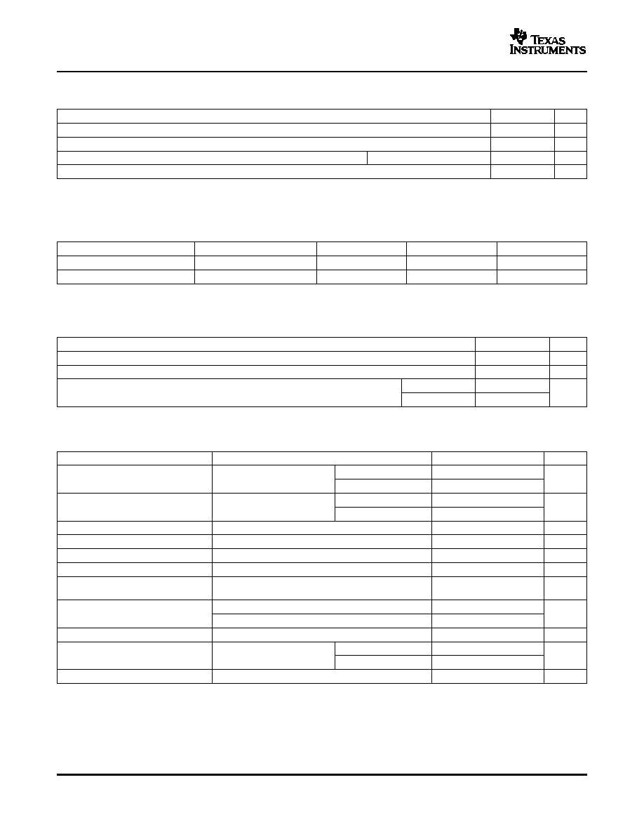
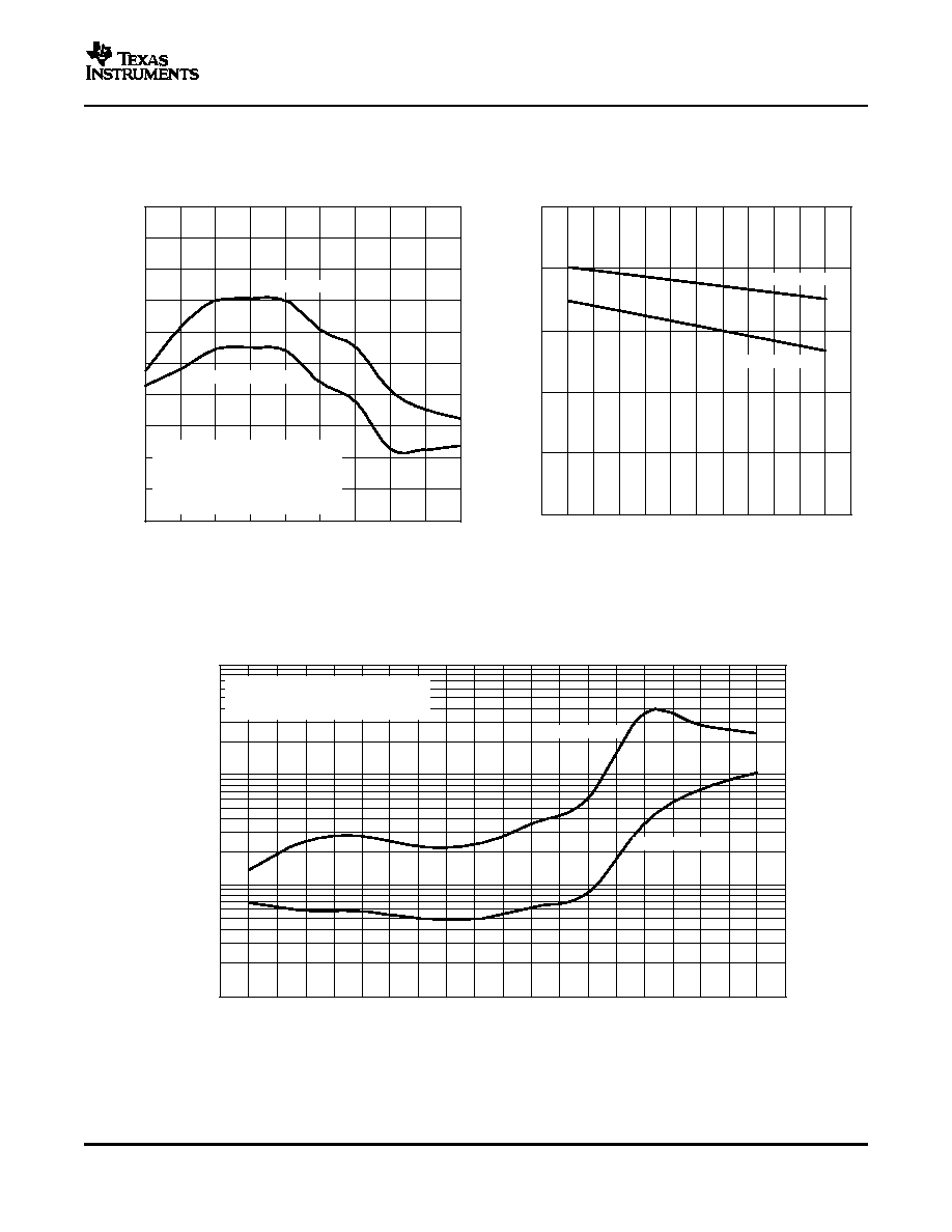
TYPICAL CHARACTERISTICS
0
25
50
75
100
125
0
0.10
0.20
0.30
0.40
0.50
0.60
0.70
0.80
0.90
1.00
T
J
- Temperature -
∞
C
V
O
-
Output V
oltage Change - %
V
I
= 4.25 V to 41.25 V
V
O
= V
ref
I
L
= 10 mA
0
25
50
T
J
- Temperature -
∞
C
V
O
-
Output V
oltage Change - %
0.20
0.15
0.10
0.05
0.00
-0.05
-0.10
-0.15
-0.20
-0.25
-0.30
-0.35
-0.40
75
100
125
V
I
= 45 V
V
O
= 5 V
I
L
= 10 mA to 100 mA
V
I
= 10 V
V
O
= 5 V
I
L
= 10 mA to 40 mA
0
25
50
53
51
49
47
45
43
41
39
37
35
ADJUST T
erminal Current -
µ
A
I
L
= 10 mA
I
L
= 100 mA
T
J
- Temperature -
∞
C
55
75
100
125
V
I
= 6.25 V
V
O
= V
ref
0
25
50
T
J
- Temperature -
∞
C
1.260
V
I
= 4.25 V
V
O
= V
ref
I
L
= 10 mA
1.255
1.250
1.245
1.240
1.235
1.230
1.225
1.220
V
ref
- Reference V
oltage - V
75
100
125
LM317M
3-TERMINAL ADJUSTABLE REGULATOR
SLVS297M ≠ APRIL 2000 ≠ REVISED OCTOBER 2005
LINE REGULATION
LOAD REGULATION
vs
vs
TEMPERATURE
TEMPERATURE
Figure 1.
Figure 2.
ADJUST TERMINAL CURRENT
TEMPERATURE STABILITY
vs
vs
TEMPERATURE
TEMPERATURE
Figure 3.
Figure 4.
3
www.ti.com
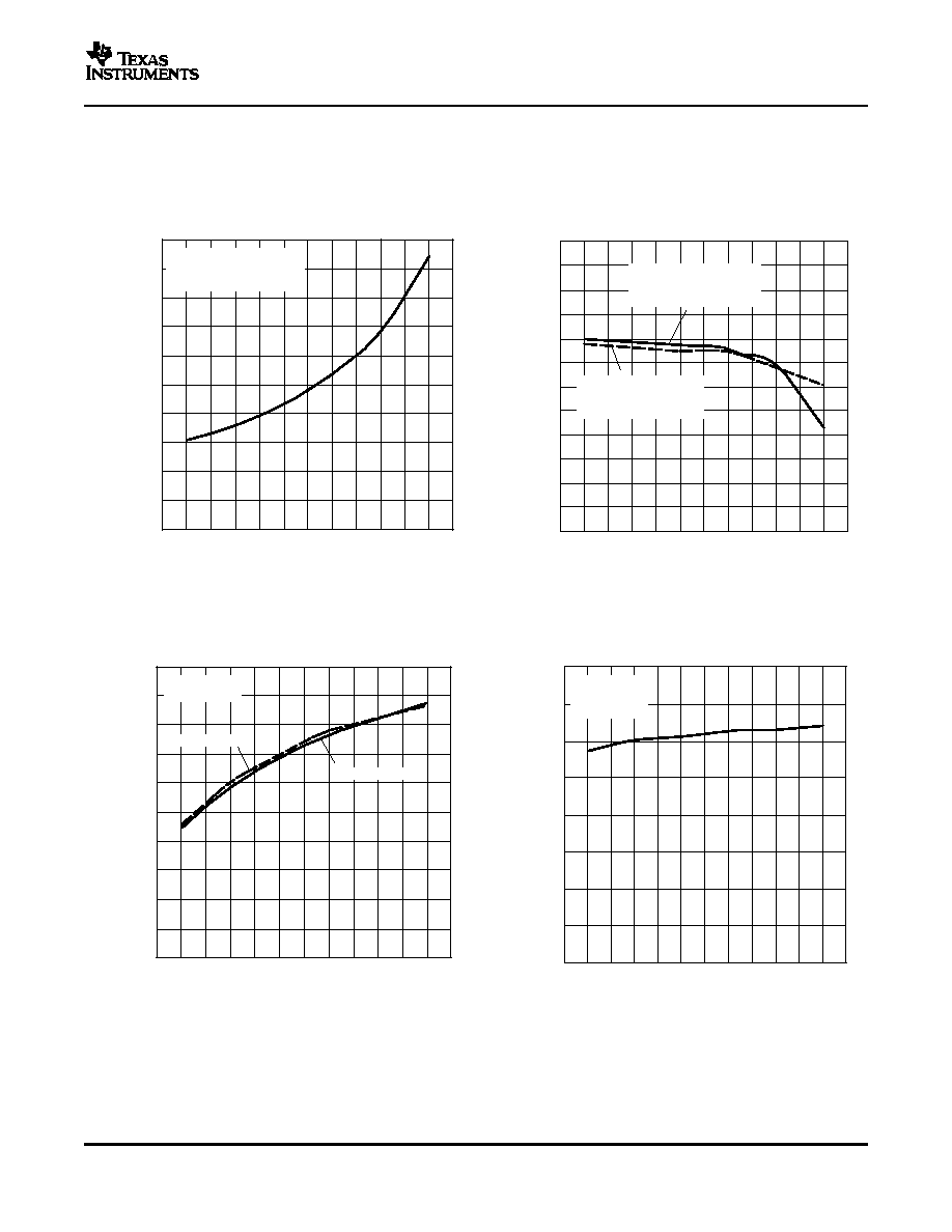
0
5
10
15
V
I
- V
O
- Input-Output Differential - V
I
1.00
0.80
0.60
0.40
0.20
0.00
O
-
Output Current -
A
T
J
= 125
∞
C
T
J
= 25
∞
C
20
25
30
35
40
0
5
10
15
20
V
I
- V
O
- Input-Output Differential - V
7
6
5
4
3
2
1
0
Minimum Operating Current - mA
T
J
= 125
∞
C
25
30
35
40
T
J
= 25
∞
C
8
0
25
50
T
J
- Temperature -
∞
C
0.004
0.003
0.002
0.001
0.000
V
I
= 15 V
V
O
= 10 V
I
L
= 50 mA
Bandwidth = 10 Hz to 10 kHz
75
100
125
% V
O
Ouput Noise V
oltage -
0
25
70
T
J
- Temperature -
∞
C
90
85
80
75
70
65
60
55
50
45
Ripple Rejection - dB
V
I
= 15 Vdc and 1 V
PP
(120 Hz)
V
O
= 10 V
I
L
= 100 mA
C
L
= 1
µ
F
C
i
= 0.1
µ
F
85
125
C
ADJ
= 0
µ
F
C
ADJ
= 10
µ
F
LM317M
3-TERMINAL ADJUSTABLE REGULATOR
SLVS297M ≠ APRIL 2000 ≠ REVISED OCTOBER 2005
TYPICAL CHARACTERISTICS (continued)
MINIMUM OPERATING CURRENT
OUTPUT CURRENT LIMIT
vs
vs
INPUT-OUTPUT DIFFERENTIAL VOLTAGE
INPUT-OUTPUT DIFFERENTIAL VOLTAGE
Figure 5.
Figure 6.
OUTPUT NOISE VOLTAGE
RIPPLE REJECTION
vs
vs
TEMPERATURE
TEMPERATURE
Figure 7.
Figure 8.
4
www.ti.com
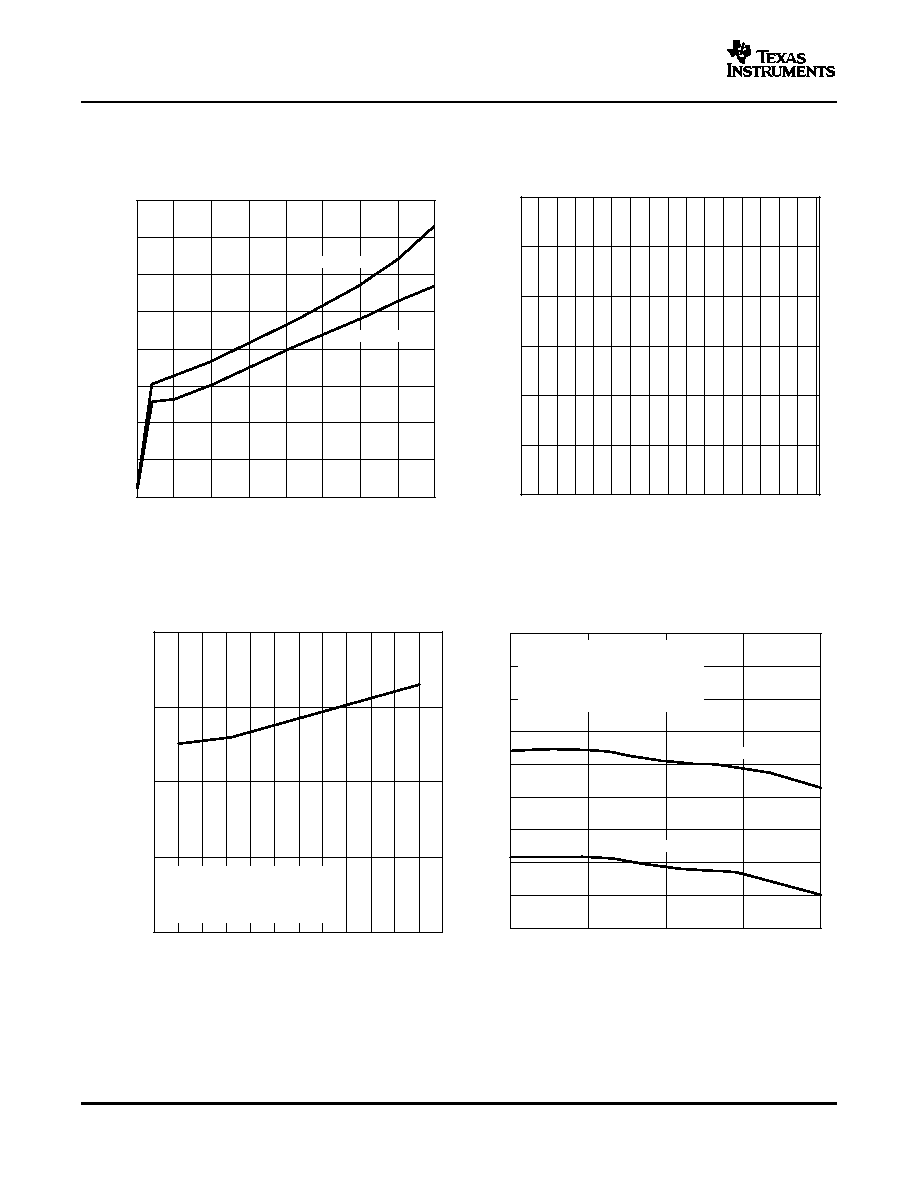
0
25
50
T
J
- Temperature -
∞
C
2.5
2
1.5
1
0.5
0
I
L
= 500 mA
I
L
= 100 mA
- V
O
(V
I
) - Input-Output V
oltage Differential - V
75
100
125
10 Hz
Frequency
100
Ripple Rejection - dB
100 Hz
1 kHz
90
80
70
60
50
40
30
20
10
0
V
I
= 15 Vdc and Vac = 1 V
PP
V
O
= 10 V
I
L
= 100 mA
C
L
= 1
µ
F
C
i
= 0.1
µ
F
C
ADJ
= 0
µ
F
C
ADJ
= 10
µ
F
10 kHz
100 kHz
10 Hz
Frequency
10.00
50 Hz
100 Hz
500 Hz
1 kHz
5 kHz
10 kHz
50 kHz
100 kHz
150 kHz
1.00
0.10
0.01
Output Impedance -
V
I
= 15 V
V
O
= 10 V
I
L
= 100-mA dc and 10-mA RMS
C
ADJ
= 0
µ
F
C
ADJ
= 10
µ
F
LM317M
3-TERMINAL ADJUSTABLE REGULATOR
SLVS297M ≠ APRIL 2000 ≠ REVISED OCTOBER 2005
TYPICAL CHARACTERISTICS (continued)
RIPPLE REJECTION
INPUT-OUTPUT VOLTAGE DIFFERENTIAL
vs
vs
FREQUENCY
TEMPERATURE
Figure 9.
Figure 10.
OUTPUT IMPEDANCE
vs
FREQUENCY
Figure 11.
5
www.ti.com
-1.0
Time -
µ
s
-0.5
0
0.5
1.0
1.5
2.0
2.5
3.0
3.5
4.0
4.5
1.2
1
0.8
0.6
0.4
0.2
0
-1
-0.8
-0.6
-0.4
-0.2
0
0.2
0.4
0.6
0.8
1
V
O
= 10 V
V
I
= 15 V,
V
I
= +1 V
I
L
= 50 mA
T
J
= 25
∞
C
C
L
= 0
µ
F
C
ADJ
= 0
µ
F
V
I
-
Input V
oltage Change - V
V
O
-
Output V
oltage Change - V
-10
Time -
µ
s
-0.2
I
O
-
Output Current Change -
A
V
O
-
Output V
oltage Change - V
-5
0
5
10
15
20
25
30
35
-0.1
0
0.1
0.2
0.3
0.4
0.5
0.6
-4.0
-3.0
-2.0
-1.0
0
1.0
2.0
3.0
4.0
5.0
V
I
= 15 V
V
O
= 10 V
I
L
= 50 mA
I
L
= +500 mA
C
L
= 1
µ
F
C
ADJ
= 10
µ
F
C
L
= 0
µ
F
C
ADJ
= 0
µ
F
LM317M
3-TERMINAL ADJUSTABLE REGULATOR
SLVS297M ≠ APRIL 2000 ≠ REVISED OCTOBER 2005
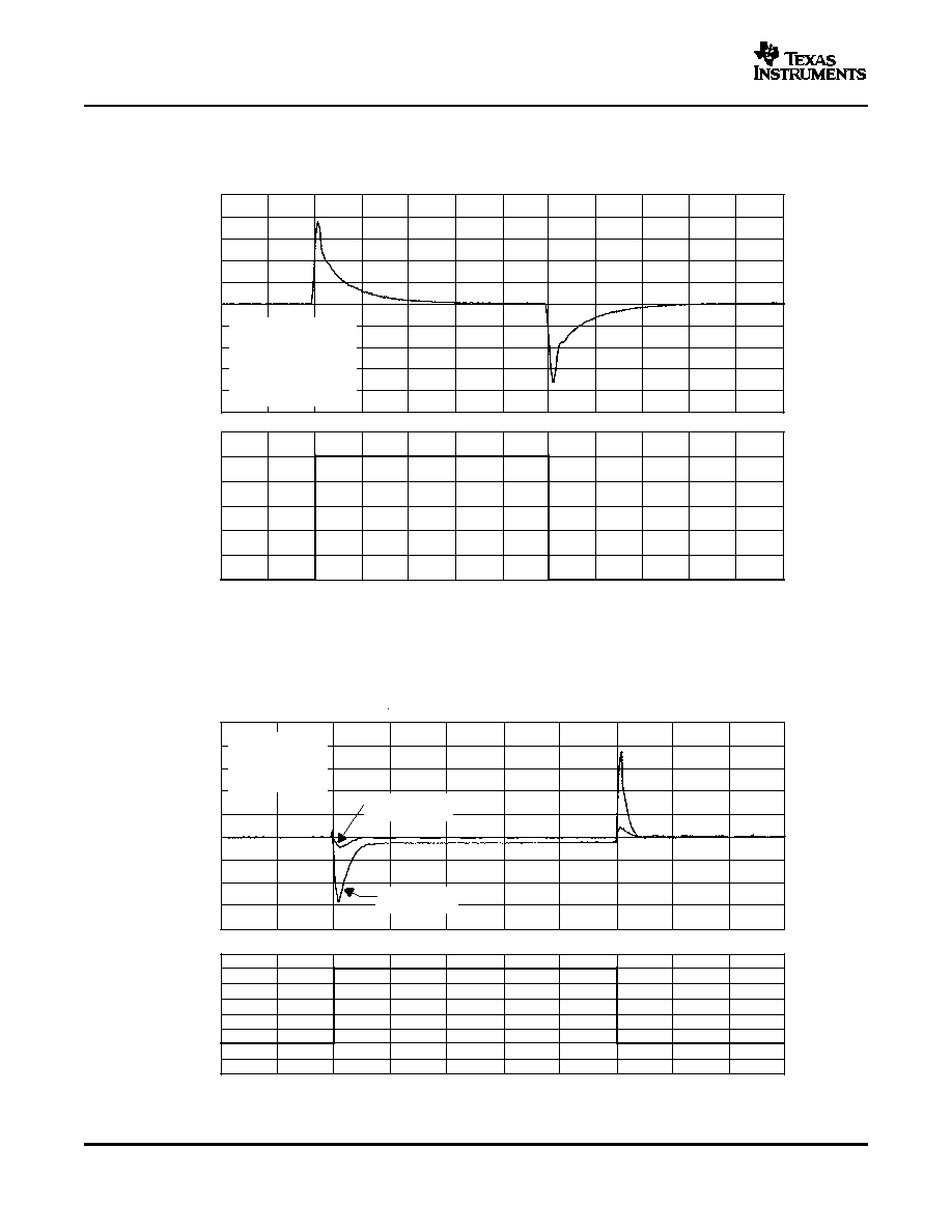
TYPICAL CHARACTERISTICS (continued)
LINE TRANSIENT RESPONSE
vs
TIME
Figure 12.
LOAD TRANSIENT RESPONSE
vs
TIME
Figure 13.
6
www.ti.com
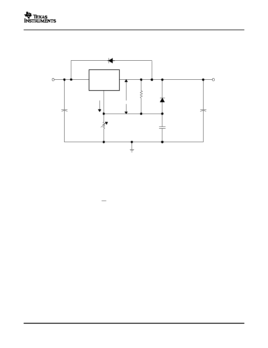
APPLICATION INFORMATION
LM317M
R
1
240
I
Adj
R
2
Adjust
C
i
(Note A)
0.1
µ
F
C
O
(Note B)
1.0
µ
F
V
I
V
O
(Note C)
NOTES: A. C
i
is not required, but is recommended, particularly if the regulator is not in close proximity
to the power-supply filter capacitors. A 0.1-
µ
F disc or 1-
µ
F tantalum provides sufficient
bypassing for most applications, especially when adjustment and output capacitors are used.
B. C
O
improves transient response, but is not needed for stability.
C. V
O
is calculated as shown:
Because I
Adj
typically is 50
µ
A, it is negligible in most applications.
D. C
ADJ
is used to improve ripple rejection; it prevents amplification of the ripple as the output voltage
is adjusted higher. If C
ADJ
is used, it is best to include protection diodes.
E. If the input is shorted to ground during a fault condition, protection diodes provide measures to
prevent the possiblility of external capacitors discharging through low-impedance paths in the IC. By
providing low-impedance discharge paths for C
O
and C
ADJ
, respectively, D1 and D2 prevent the
capacitors from discharging into the output of the regulator.
Output
Input
V
ref
= 1.25 V
V
O
+
V
ref
1
)
R
2
R
1
) (
I
Adj
R
2
)
D1
(Note E)
1N4002
D2
(Note E)
1N4002
C
ADJ
(Note D)
LM317M
3-TERMINAL ADJUSTABLE REGULATOR
SLVS297M ≠ APRIL 2000 ≠ REVISED OCTOBER 2005
Figure 14. Adjustable Voltage Regulator
7
PACKAGING INFORMATION
Orderable Device
Status
(1)
Package
Type
Package
Drawing
Pins Package
Qty
Eco Plan
(2)
Lead/Ball Finish
MSL Peak Temp
(3)
LM317MDCY
ACTIVE
SOT-223
DCY
4
80
TBD
CU SNPB
Level-2-235C-1 YEAR
LM317MDCYG3
ACTIVE
SOT-223
DCY
4
80
Green (RoHS &
no Sb/Br)
CU SN
Level-2-260C-1YEAR
LM317MDCYR
ACTIVE
SOT-223
DCY
4
2500
TBD
CU SNPB
Level-2-235C-1 YEAR
LM317MDCYRG3
ACTIVE
SOT-223
DCY
4
2500 Green (RoHS &
no Sb/Br)
CU SN
Level-2-260C-1YEAR
LM317MKTPR
ACTIVE
PFM
KTP
2
3000
TBD
CU SNPB
Level-1-220C-UNLIM
LM317MKTPRG3
ACTIVE
PFM
KTP
2
3000 Green (RoHS &
no Sb/Br)
CU SN
Level-1-260C-UNLIM
LM317MQDCYR
ACTIVE
SOT-223
DCY
4
2500
TBD
SNPB
Level-2-235C-1 YEAR
LM317MQDCYRG3
ACTIVE
SOT-223
DCY
4
2500 Green (RoHS &
no Sb/Br)
CU SN
Level-2-260C-1 YEAR
LM317MQKTPR
ACTIVE
PFM
KTP
2
3000
TBD
CU SNPB
Level-1-220C-UNLIM
(1)
The marketing status values are defined as follows:
ACTIVE: Product device recommended for new designs.
LIFEBUY: TI has announced that the device will be discontinued, and a lifetime-buy period is in effect.
NRND: Not recommended for new designs. Device is in production to support existing customers, but TI does not recommend using this part in
a new design.
PREVIEW: Device has been announced but is not in production. Samples may or may not be available.
OBSOLETE: TI has discontinued the production of the device.
(2)
Eco
Plan
-
The
planned
eco-friendly
classification:
Pb-Free
(RoHS)
or
Green
(RoHS
&
no
Sb/Br)
-
please
check
http://www.ti.com/productcontent
for the latest availability information and additional product content details.
TBD: The Pb-Free/Green conversion plan has not been defined.
Pb-Free (RoHS): TI's terms "Lead-Free" or "Pb-Free" mean semiconductor products that are compatible with the current RoHS requirements
for all 6 substances, including the requirement that lead not exceed 0.1% by weight in homogeneous materials. Where designed to be soldered
at high temperatures, TI Pb-Free products are suitable for use in specified lead-free processes.
Green (RoHS & no Sb/Br): TI defines "Green" to mean Pb-Free (RoHS compatible), and free of Bromine (Br) and Antimony (Sb) based flame
retardants (Br or Sb do not exceed 0.1% by weight in homogeneous material)
(3)
MSL, Peak Temp. -- The Moisture Sensitivity Level rating according to the JEDEC industry standard classifications, and peak solder
temperature.
Important Information and Disclaimer:The information provided on this page represents TI's knowledge and belief as of the date that it is
provided. TI bases its knowledge and belief on information provided by third parties, and makes no representation or warranty as to the
accuracy of such information. Efforts are underway to better integrate information from third parties. TI has taken and continues to take
reasonable steps to provide representative and accurate information but may not have conducted destructive testing or chemical analysis on
incoming materials and chemicals. TI and TI suppliers consider certain information to be proprietary, and thus CAS numbers and other limited
information may not be available for release.
In no event shall TI's liability arising out of such information exceed the total purchase price of the TI part(s) at issue in this document sold by TI
to Customer on an annual basis.
PACKAGE OPTION ADDENDUM
www.ti.com
18-Oct-2005
Addendum-Page 1
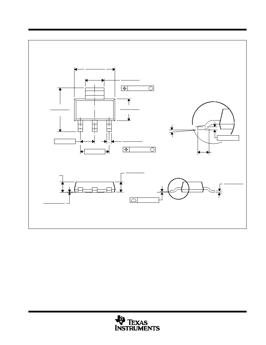
MECHANICAL DATA
MPDS094A ≠ APRIL 2001 ≠ REVISED JUNE 2002
POST OFFICE BOX 655303
∑
DALLAS, TEXAS 75265
DCY (R-PDSO-G4)
PLASTIC SMALL-OUTLINE
4202506/B 06/2002
6,30 (0.248)
6,70 (0.264)
2,90 (0.114)
3,10 (0.122)
6,70 (0.264)
7,30 (0.287)
3,70 (0.146)
3,30 (0.130)
0,02 (0.0008)
0,10 (0.0040)
1,50 (0.059)
1,70 (0.067)
0,23 (0.009)
0,35 (0.014)
1
2
3
4
0,66 (0.026)
0,84 (0.033)
1,80 (0.071) MAX
Seating Plane
0
∞
≠10
∞
Gauge Plane
0,75 (0.030) MIN
0,25 (0.010)
0,08 (0.003)
0,10 (0.004) M
2,30 (0.091)
4,60 (0.181)
M
0,10 (0.004)
NOTES: A. All linear dimensions are in millimeters (inches).
B. This drawing is subject to change without notice.
C. Body dimensions do not include mold flash or protrusion.
D. Falls within JEDEC TO-261 Variation AA.
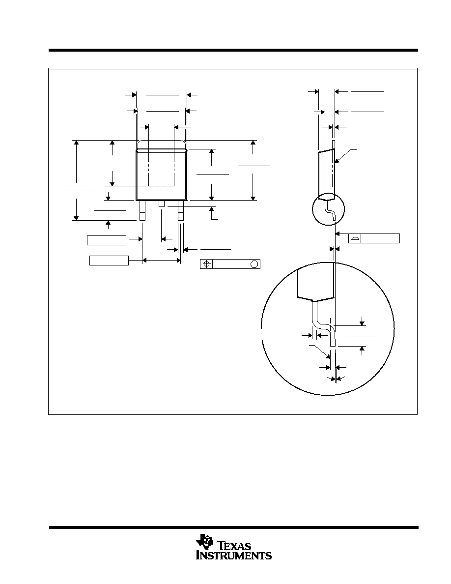
MECHANICAL DATA
MPSF001F ≠ JANUARY 1996 ≠ REVISED JANUARY 2002
1
POST OFFICE BOX 655303
∑
DALLAS, TEXAS 75265
KTP (R-PSFM-G2)
PowerFLEX
PLASTIC FLANGE-MOUNT PACKAGE
0.228 (5,79)
0.218 (5,54)
0.233 (5,91)
0.243 (6,17)
0.001 (0,02)
0.005 (0,13)
0.070 (1,78)
Seating Plane
0.080 (2,03)
0.010 (0,25) NOM
Gage Plane
0.010 (0,25)
4073388/M 01/02
0.037 (0,94)
0.047 (1,19)
0.247 (6,27)
0.237 (6,02)
NOM
0.215 (5,46)
0.371 (9,42)
0.381 (9,68)
0.090 (2,29)
0.100 (2,54)
0.287 (7,29)
0.031 (0,79)
0.032 (0,81) MAX
0.277 (7,03)
0.025 (0,63)
0.130 (3,30) NOM
0.090 (2,29)
0.180 (4,57)
M
0.010 (0,25)
0.004 (0,10)
2
∞
≠ 6
∞
0.040 (1,02)
0.050 (1,27)
Thermal Tab
(See Note C)
0.010 (0,25) NOM
NOTES: A. All linear dimensions are in inches (millimeters).
B. This drawing is subject to change without notice.
C. The center lead is in electrical contact with the thermal tab.
D. Dimensions do not include mold protrusions, not to exceed 0.006 (0,15).
E. Falls within JEDEC TO-252 variation AC.
PowerFLEX is a trademark of Texas Instruments.

IMPORTANT NOTICE
Texas Instruments Incorporated and its subsidiaries (TI) reserve the right to make corrections, modifications,
enhancements, improvements, and other changes to its products and services at any time and to discontinue
any product or service without notice. Customers should obtain the latest relevant information before placing
orders and should verify that such information is current and complete. All products are sold subject to TI's terms
and conditions of sale supplied at the time of order acknowledgment.
TI warrants performance of its hardware products to the specifications applicable at the time of sale in
accordance with TI's standard warranty. Testing and other quality control techniques are used to the extent TI
deems necessary to support this warranty. Except where mandated by government requirements, testing of all
parameters of each product is not necessarily performed.
TI assumes no liability for applications assistance or customer product design. Customers are responsible for
their products and applications using TI components. To minimize the risks associated with customer products
and applications, customers should provide adequate design and operating safeguards.
TI does not warrant or represent that any license, either express or implied, is granted under any TI patent right,
copyright, mask work right, or other TI intellectual property right relating to any combination, machine, or process
in which TI products or services are used. Information published by TI regarding third-party products or services
does not constitute a license from TI to use such products or services or a warranty or endorsement thereof.
Use of such information may require a license from a third party under the patents or other intellectual property
of the third party, or a license from TI under the patents or other intellectual property of TI.
Reproduction of information in TI data books or data sheets is permissible only if reproduction is without
alteration and is accompanied by all associated warranties, conditions, limitations, and notices. Reproduction
of this information with alteration is an unfair and deceptive business practice. TI is not responsible or liable for
such altered documentation.
Resale of TI products or services with statements different from or beyond the parameters stated by TI for that
product or service voids all express and any implied warranties for the associated TI product or service and
is an unfair and deceptive business practice. TI is not responsible or liable for any such statements.
Following are URLs where you can obtain information on other Texas Instruments products and application
solutions:
Products
Applications
Amplifiers
amplifier.ti.com
Audio
www.ti.com/audio
Data Converters
dataconverter.ti.com
Automotive
www.ti.com/automotive
DSP
dsp.ti.com
Broadband
www.ti.com/broadband
Interface
interface.ti.com
Digital Control
www.ti.com/digitalcontrol
Logic
logic.ti.com
Military
www.ti.com/military
Power Mgmt
power.ti.com
Optical Networking
www.ti.com/opticalnetwork
Microcontrollers
microcontroller.ti.com
Security
www.ti.com/security
Telephony
www.ti.com/telephony
Video & Imaging
www.ti.com/video
Wireless
www.ti.com/wireless
Mailing Address:
Texas Instruments
Post Office Box 655303 Dallas, Texas 75265
Copyright
2005, Texas Instruments Incorporated