Document Outline
- FEATURES
- APPLICATIONS
- DESCRIPTION
- ABSOLUTE MAXIMUM RATINGS
- PACKAGE/ORDERING INFORMATION
- PIN CONFIGURATION
- ELECTRICAL CHARACTERISTICS
- TYPICAL CHARACTERISTICS
- APPLICATION INFORMATION
- INPUT CURRENT RANGE
- SETTING THE REFERENCE CURRENT
- FREQUENCY COMPENSATION
- FREQUENCY RESPONSE
- NEGATIVE INPUT CURRENTS
- VOLTAGE INPUTS
- ACHIEVING HIGHER ACCURACY WITH HIGHER INPUT CURRENTS
- APPLICATION CIRCUITS
- LOG RATIO
- DATA COMPRESSION
- OPERATION ON SINGLE SUPPLY
- MEASURING AVALANCHE PHOTODIODE CURRENT
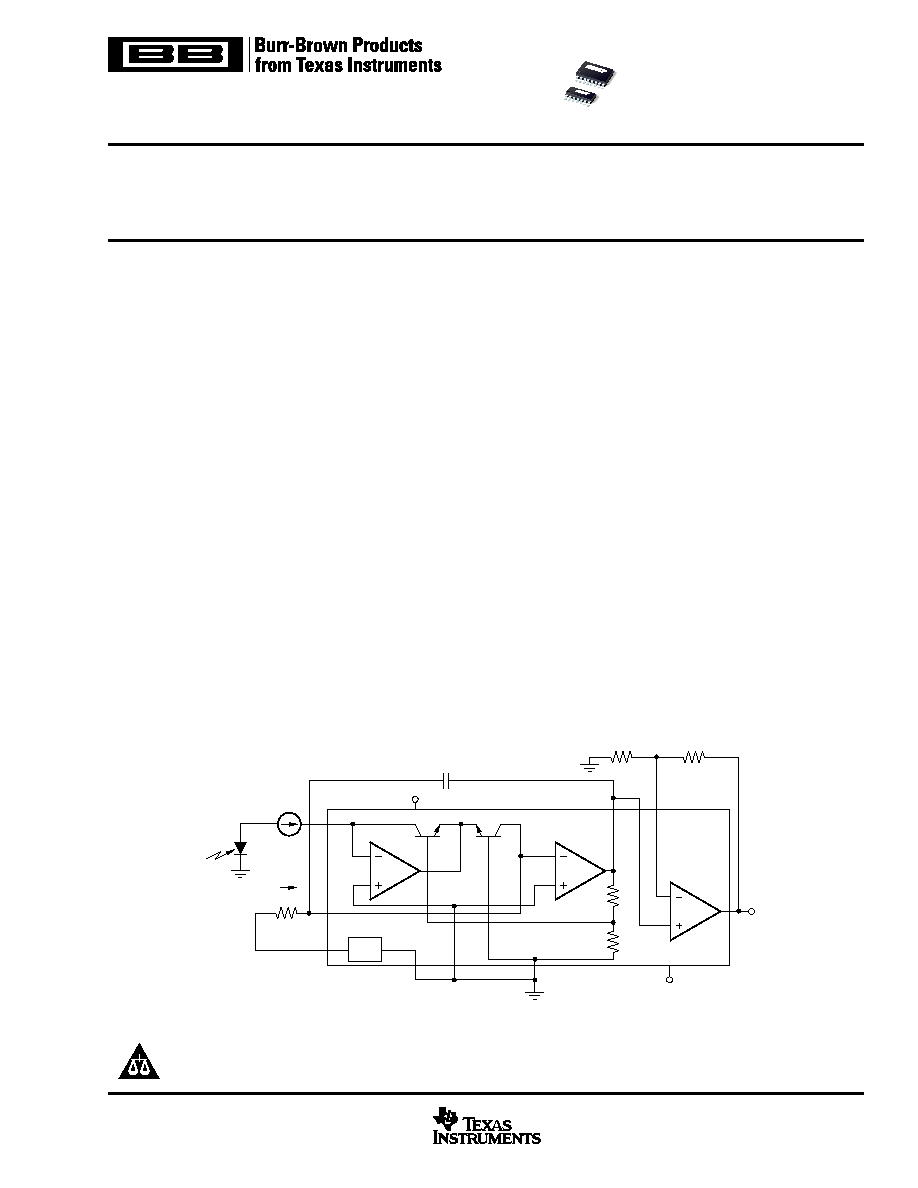
- INSIDE THE LOG112
- DEFINITION OF TERMS
- TRANSFER FUNCTION
- ACCURACY
- TOTAL ERROR
- ERRORS RTO AND RTI
- LOG CONFORMITY
- INDIVIDUAL ERROR COMPONENTS
- PACKAGE DRAWINGS
- D (R-PDSO-G**) PLASTIC SMALL-OUTLINE PACKAGE
- DW (R-PDSO-G**) PLASTIC SMALL-OUTLINE PACKAGE
LOG112
LOG2112
SBOS246C ≠ JUNE 2002 ≠ REVISED APRIL 2003
www.ti.com
DESCRIPTION
The LOG112 and LOG2112 are versatile integrated circuits
that compute the logarithm or log ratio of an input current
relative to a reference current. V
LOGOUT
of the LOG112 and
LOG2112 are trimmed to 0.5V per decade of input current,
ensuring high precision over a wide dynamic range of input
signals.
The LOG112 and LOG2112 features a 2.5V voltage refer-
ence that may be used to generate a precision current
reference using an external resistor.
Low DC offset voltage and temperature drift allow accurate
measurement of low-level signals over the specified tem-
perature range of ≠5
∞
C to +75
∞
C.
FEATURES
q
EASY-TO-USE COMPLETE FUNCTION
q
OUTPUT SCALING AMPLIFIER
q
ON-CHIP 2.5V VOLTAGE REFERENCE
q
HIGH ACCURACY: 0.2% FSO Over 5 Decades
q
WIDE INPUT DYNAMIC RANGE:
7.5 Decades, 100pA to 3.5mA
q
LOW QUIESCENT CURRENT: 1.75mA
q
WIDE SUPPLY RANGE:
±
4.5V to
±
18V
q
PACKAGES: SO-14 (narrow) and SO-16
PRODUCTION DATA information is current as of publication date.
Products conform to specifications per the terms of Texas Instruments
standard warranty. Production processing does not necessarily include
testing of all parameters.
Copyright © 2002-2003, Texas Instruments Incorporated
Precision
LOGARITHMIC AND LOG RATIO AMPLIFIERS
Please be aware that an important notice concerning availability, standard warranty, and use in critical applications of
Texas Instruments semiconductor products and disclaimers thereto appears at the end of this data sheet.
APPLICATIONS
q
LOG, LOG RATIO:
Communication, Analytical, Medical, Industrial,
Test, General Instrumentation
q
PHOTODIODE SIGNAL COMPRESSION AMP
q
ANALOG SIGNAL COMPRESSION IN FRONT
OF ANALOG-TO-DIGITAL (A/D) CONVERTER
q
ABSORBANCE MEASUREMENT
q
OPTICAL DENSITY MEASUREMENT
LOG1
12
LOG2
112
A
2
A
1
Q
1
Q
2
C
C
I
1
V
REF ≠ GND
NOTE: Internal resistors are used to compensate gain change over temperature.
The V
CM
pin is internally connected to GND in the LOG2112.
V
O3
V+
GND
LOG112
V
LOGOUT
= (0.5V)LOG (I
1
/I
2
)
V
O3
= K (0.5V)LOG (I
1
/I
2
), K = 1 + R
2
/R
1
A
3
R
2
R
1
V
REF
R
REF
+IN3
V
LOGOUT
≠IN3
V≠
V
CM
I
2
V
REF
LOG112, 2112
2
SBOS246C
www.ti.com
ABSOLUTE MAXIMUM RATINGS
(1)
Supply Voltage, V+ to V≠ ..................................................................
±
18V
Inputs .................................................................................................
±
18V
Input Current ...................................................................................
±
10mA
Output Short-Circuit Current
(2)
................................................ Continuous
Operating Temperature .................................................... ≠40
∞
C to +85
∞
C
Storage Temperature ..................................................... ≠55
∞
C to +125
∞
C
Junction Temperature .................................................................... +150
∞
C
Lead Temperature (soldering, 10s) ............................................... +300
∞
C
NOTES: (1) Stresses above these ratings may cause permanent damage.
Exposure to absolute maximum conditions for extended periods may degrade
device reliability. (2) One output per package.
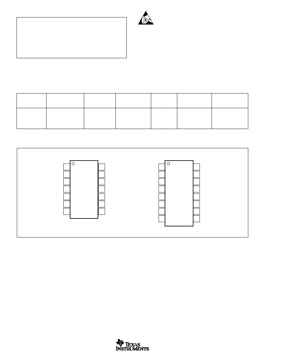
PIN CONFIGURATION
Top View
SO
I
2
V
CM ≠ IN
NC
V
REF ≠ GND
GND
V≠
V
REF
NC = No Internal Connection
LOG112
I
1
NC
+IN3
≠IN3
V
LOGOUT
V+
V
O3
14
13
12
11
10
9
8
1
2
3
4
5
6
7
I
1B
I
2B
+IN3B
≠IN3B
V
LOGOUTB
V≠
V
03B
V
REF
LOG2112
I
1A
I
2A
+IN3A
≠IN3A
V
LOGOUTA
V+
V
O3A
GND
16
15
14
13
12
11
10
9
1
2
3
4
5
6
7
8
ELECTROSTATIC
DISCHARGE SENSITIVITY
This integrated circuit can be damaged by ESD. Texas Instru-
ments recommends that all integrated circuits be handled with
appropriate precautions. Failure to observe proper handling
and installation procedures can cause damage.
ESD damage can range from subtle performance degradation
to complete device failure. Precision integrated circuits may be
more susceptible to damage because very small parametric
changes could cause the device not to meet its published
specifications.
SPECIFIED
PACKAGE
TEMPERATURE
PACKAGE
ORDERING
TRANSPORT
PRODUCT
PACKAGE-LEAD
DESIGNATOR
(1)
RANGE
MARKING
NUMBER
MEDIA, QUANTITY
LOG112
SO-14
D
≠5
∞
C to +75
∞
C
LOG112A
LOG112AID
Rails, 250
"
"
"
"
"
LOG112AIDR
Tape and Reel, 2500
LOG2112
SO-16
DW
≠5
∞
C to +75
∞
C
LOG2112A
LOG2112AIDW
Rails, 250
"
"
"
"
"
LOG2112AIDWR
Tape and Reel, 2500
NOTE: (1) For the most current specifications and package information, refer to our web site at www.ti.com.
PACKAGE/ORDERING INFORMATION
LOG112, 2112
3
SBOS246C
www.ti.com
ELECTRICAL CHARACTERISTICS
Boldface limits apply over the specified temperature range, T
A
= ≠5
∞
C to +75
∞
C.
At T
A
= +25
∞
C, V
S
=
±
5V, and R
OUT
= 10k
, unless otherwise noted.
LOG112, LOG2112
PARAMETER
CONDITION
MIN
TYP
MAX
UNITS
CORE LOG FUNCTION
V
IN
/ V
OUT
Equation
V
LOGOUT
= (0.5V)LOG (I
1
/I
2
)
V
LOG CONFORMITY ERROR
(1)
Initial
1nA to 100
µ
A (5 decades)
0.01
0.2
%
100pA to 3.5mA (7.5 decades)
0.13
%
over Temperature
1nA to 100
µ
A (5 decades)
0.0001
%/
∞
C
100pA to 3.5mA (7.5 decades)
0.005
%/
∞
C
GAIN
(2)
Initial Value
1nA to 100
µ
A
0.5
V/decade
Gain Error
1nA to 100
µ
A
0.10
±
1
%
vs Temperature
T
MIN
to T
MAX
0.003
0.01
%/
∞
C
INPUT, A
1A
and A
1B
, A
2A
, A
2B
Offset Voltage
±
0.3
±
1.5
mV
vs Temperature
T
MIN
to T
MAX
±
2
µ
V/
∞
C
vs Power Supply (PSRR)
V
S
=
±
4.5V to
±
18V
5
20
µ
V/V
Input Bias Current
±
5
pA
vs Temperature
T
MIN
to T
MAX
Doubles Every 10
∞
C
Voltage Noise
f = 10Hz to 10kHz
3
µ
Vrms
f = 1kHz
30
nV/
Hz
Current Noise
f = 1kHz
4
fA/
Hz
Common-Mode Voltage Range (Positive)
(V+) ≠ 2
(V+) ≠ 1.5
V
(Negative)
(V≠) + 2
(V≠) + 1.2
V
Common-Mode Rejection Ratio (CMRR)
10
µ
V/V
OUTPUT, (V
LOG OUT
) A
2A
, A
2B
Output Offset, V
OSO
, Initial
±
3
±
15
mV
vs Temperature
T
MIN
to T
MAX
±
10
µ
V/
∞
C
Full-Scale Output (FSO)
V
S
=
±
5V
(V≠) + 1.2
(V+) ≠ 1.5
V
Short-Circuit Current
±
18
mA
TOTAL ERROR
(3)(4)
I
1
or I
2
remains fixed while other varies.
Initial
Min to Max
I
1
or I
2
= 5mA (V
S
±
6V)
±
150
mV
I
1
or I
2
= 3.5mA
±
75
mV
I
1
or I
2
= 1mA
±
20
mV
I
1
or I
2
= 100
µ
A
±
20
mV
I
1
or I
2
= 10
µ
A
±
20
mV
I
1
or I
2
= 1
µ
A
±
20
mV
I
1
or I
2
= 100nA
±
20
mV
I
1
or I
2
= 10nA
±
20
mV
I
1
or I
2
= 1nA
±
20
mV
I
1
or I
2
= 350pA
±
20
mV
I
1
or I
2
= 100pA
±
20
mV
vs Temperature
I
1
or I
2
= 3.5mA
±
1.2
mV/
∞
C
I
1
or I
2
= 1mA
±
0.4
mV/
∞
C
I
1
or I
2
= 100
µ
A
±
0.1
mV/
∞
C
I
1
or I
2
= 10
µ
A
±
0.05
mV/
∞
C
I
1
or I
2
= 1
µ
A
±
0.05
mV/
∞
C
I
1
or I
2
= 100nA
±
0.09
mV/
∞
C
I
1
or I
2
= 10nA
±
0.2
mV/
∞
C
I
1
or I
2
= 1nA
±
0.3
mV/
∞
C
I
1
or I
2
= 350pA
±
0.1
mV/
∞
C
I
1
or I
2
= 100pA
±
0.3
mV/
∞
C
vs Supply
I
1
or I
2
= 3.5mA
±
3.0
mV/ V
I
1
or I
2
= 1mA
±
0.1
mV/ V
I
1
or I
2
= 100
µ
A
±
0.1
mV/ V
I
1
or I
2
= 10
µ
A
±
0.1
mV/ V
I
1
or I
2
= 1
µ
A
±
0.1
mV/ V
I
1
or I
2
= 100nA
±
0.1
mV/ V
I
1
or I
2
= 10nA
±
0.1
mV/ V
I
1
or I
2
= 1nA
±
0.25
mV/V
I
1
or I
2
= 350pA
±
0.1
mV/ V
I
1
or I
2
= 100pA
±
0.1
mV/ V
NOTES: (1) Log Conformity Error is the peak deviation from the best-fit-straight line of V
O
versus LOG (I
1
/I
2
) curve expressed as a percent of peak-to-peak full-
scale output. K, scale factor, equals 0.5V output per decade of input current. (2) Scale factor of core log function is trimmed to 0.5V output per decade change of
input current. (3) Worst-case Total Error for any ratio of I
1
/I
2
, as the largest of the two errors, when I
1
and I
2
are considered separately. (4) Total Error includes offset
voltage, bias current, gain, and log conformity. (5) Bandwidth (3dB) and transient response are a function of both the compensation capacitor and the level of input
current.

LOG112, 2112
4
SBOS246C
www.ti.com
FREQUENCY RESPONSE, CORE LOG
(5)
BW, 3dB
I
2
= 10nA
C
C
= 4500pF
0.1
kH
I
2
= 1
µ
A
C
C
= 150pF
38
kH
I
2
= 10
µ
A
C
C
= 150pF
40
kH
I
2
= 1mA
C
C
= 50pF
45
kHz
Step Response
Increasing
I
1
= 10nA to 100nA
C
C
= 120pF, I
2
= 31.6nA
1.1
ms
I
1
= 1
µ
A to 100
µ
A
C
C
= 375pF, I
2
= 10
µ
A
1.6
µ
s
I
1
= 1
µ
A to 1mA
C
C
= 950pF, I
2
= 31.6
µ
A
1.5
µ
s
Decreasing
I
1
= 100nA to 10nA
C
C
= 120pF, I
2
= 31.6nA
2.1
ms
I
1
= 100
µ
A to 1
µ
A
C
C
= 375pF, I
2
= 10
µ
A
31.2
µ
s
I
1
= 1mA to 1
µ
A
C
C
= 950pF, I
2
= 31.6
µ
A
39
µ
s
Increasing
I
2
= 10nA to 100nA
C
C
= 125pF, I
1
= 31.6nA
2.6
ms
I
2
= 1
µ
A to 100
µ
A
C
C
= 750pF, I
1
= 10
µ
A
113
µ
s
I
2
= 1
µ
A to 1mA
C
C
= 10.5nF, I
1
= 31.6
µ
A
1.2
ms
Decreasing
I
2
= 100nA to 10nA
C
C
= 125pF, I
1
= 31.6nA
630
µ
s
I
2
= 100
µ
A to 1
µ
A
C
C
= 750pF, I
1
= 10
µ
A
6.6
µ
s
I
2
= 1mA to 1
µ
A
C
C
= 10.5nF, I
1
= 31.6
µ
A
13.3
µ
s
OP AMP, A3
Input Offset Voltage
+250
±
1000
µ
V
vs Temperature
T
MIN
to T
MAX
±
2
µ
V/
∞
C
vs Supply
V
S
=
±
4.5V to
±
18V
5
50
µ
V/V
Input Bias Current
≠10
nA
Input Offset Current
±
0.5
nA
Input Voltage Range
(V≠)
(V+) ≠ 1.5
V
Input Noise, f = 0.1Hz to 10Hz
1
µ
Vp-p
f = 1kHz
28
nV/
Hz
Open-Loop Voltage Gain
88
dB
Gain-Bandwidth Product
1.4
MHz
Slew Rate
0.5
V/
µ
s
Settling Time, 0.01%
G = ≠1, 3V Step, C
L
= 100pF
16
µ
s
Rated Output
(V≠) + 1.5
(V+) ≠ 0.9
V
Short-Circuit Current
±
4
mA
VOLTAGE REFERENCE
Bandgap Voltage
2.5
V
Error, Initial
±
0.05
±
0.5
%
vs Temperature
T
MIN
to T
MAX
±
25
ppm/
∞
C
vs Supply
V
S
=
±
4.5V to
±
18V
±
10
ppm/V
vs Load
I
LOAD
= 10mA
±
600
ppm/mA
Short-Circuit Current
16
mA
POWER SUPPLY
Operating Range
V
S
±
4.5
±
18
V
Quiescent Current
I
O
= 0
LOG112
±
1.25
±
1.75
mA
LOG2112
±
2.5
±
3.5
mA
TEMPERATURE RANGE
Specified Range, T
MIN
to T
MAX
≠5
75
∞
C
Operating Range
≠40
85
∞
C
Storage Range
≠55
125
∞
C
Thermal Resistance,
JA
SO-14
110
∞
C/W
SO-16
80
∞
C/W
NOTES: (1) Log Conformity Error is the peak deviation from the best-fit-straight line of V
O
vs LOG(I
1
/I
2
) curve expressed as a percent of peak-to-peak full-scale
output. K, scale factor, equals 0.5V output per decade of input current. (2) Scale factor of core log function is trimmed to 0.5V output per decade change of input
current. (3) Worst-case Total Error for any ratio of I
1
/I
2
, as the largest of the two errors, when I
1
and I
2
are considered separately. (4) Total Error includes offset
voltage, bias current, gain, and log conformity. (5) Bandwidth (3dB) and transient response are a function of both the compensation capacitor and the level of input
current.
ELECTRICAL CHARACTERISTICS
(Cont.)
Boldface limits apply over the specified temperature range, T
A
= ≠5
∞
C to +75
∞
C.
At T
A
= +25
∞
C, V
S
=
±
5V, and R
L
= 10k
, unless otherwise noted.
LOG112, LOG2112
PARAMETER
CONDITION
MIN
TYP
MAX
UNITS
LOG112, 2112
5
SBOS246C
www.ti.com
TYPICAL CHARACTERISTICS
At T
A
= +25
∞
C, V
S
=
±
5V, and R
L
= 10k
, unless otherwise noted.
2.0
1.5
1.0
0.5
0
≠0.5
≠1.0
≠1.5
≠2.0
Normalized Output V
oltage (V)
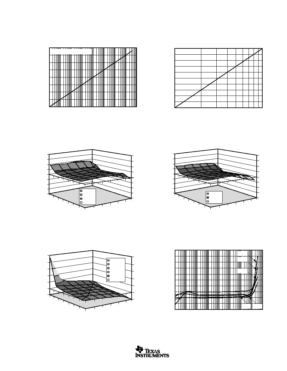
NORMALIZED TRANSFER FUNCTION
0.0001 0.001
0.01
0.1
1
10
100
1k
10k
Current Ratio, I
1
/I
2
V
LOGOUT
= (0.5V)LOG (I
1
/I
2
)
ONE CYCLE OF NORMALIZED TRANSFER FUNCTION
Normalized Output Voltage (V)
0.50
0.45
0.40
0.35
0.30
0.25
0.20
0.15
0.10
0.05
0
1
10
Current Ratio, I
1
/I
2
8
7
6
5
4
3
2
1
0
≠1
≠2
1nA
10nA 100nA 1
µ
A
10
µ
A 100
µ
A 1mA
10mA
100pA
GAIN ERROR (I
2
= 1
µ
A)
Input Current (I
1
or I
2
)
Gain Error (%)
≠40
∞
C
+75
∞
C
≠5
∞
C +25
∞
C
+85
∞
C
≠20
≠15
≠10
≠5
0
5
10
15
20
≠20
≠15
≠10
≠5
0
5
10
15
20
1mA
10
µ
A
100nA
1nA
10nA
100nA
1
µ
A
10
µ
A
100
µ
A
1mA
1nA
I
1
I
2
Total Error (mV)
TOTAL ERROR (≠5
∞
C)
Total Error (mV)
10 to 15
5 to 10
0 to 5
≠5 to 0
≠20
≠15
≠10
≠5
0
5
10
15
20
≠20
≠15
≠10
≠5
0
5
10
15
20
1mA
10
µ
A
100
µ
A
1
µ
A
100nA
1nA
10nA
100nA
1
µ
A
10
µ
A
100
µ
A
1mA
10nA
1nA
I
1
I
2
Total Error (mV)
Total Error (mV)
5 to 10
0 to 5
≠5 to 0
TOTAL ERROR (25
∞
C)
≠20
20
0
40
60
80
100
≠20
0
20
40
60
80
100
1mA
10
µ
A
100
µ
A
1
µ
A
100nA
1nA
10nA
100nA
1
µ
A
10
µ
A
100
µ
A
1mA
10nA
1nA
I
1
I
2
Total Error (mV)
Total Error (mV)
20 to 40
0 to 20
40 to 60
60 to 80
80 to 100
≠20 to 0
TOTAL ERROR (70
∞
C)