 | –≠–ª–µ–∫—Ç—Ä–æ–Ω–Ω—ã–π –∫–æ–º–ø–æ–Ω–µ–Ω—Ç: LP239 | –°–∫–∞—á–∞—Ç—å:  PDF PDF  ZIP ZIP |
LP239, LP339, LP2901
LOW-POWER QUAD DIFFERENTIAL COMPARATORS
SLCS004A ≠ OCTOBER 1987 ≠ REVISED MAY 1988
1
POST OFFICE BOX 655303
∑
DALLAS, TEXAS 75265
D
Ultralow Power Supply Current
Drain . . . 60
µ
A Typ
D
Low Input Biasing Current . . . 3
nA
D
Low Input Offset Current . . .
±
0.5
nA
D
Low Input Offset Voltage . . .
±
2 mV
D
Common-Mode Input Voltage Includes
Ground
D
Output Voltage Compatible With MOS and
CMOS Logic
D
High Output Sink-Current Capability
(30 mA at V
O
= 2V)
D
Power Supply Input Reverse-Voltage
Protected
D
Single-Power-Supply Operation
D
Pin-for-Pin Compatible With LM239, LM339,
LM2901
description
The LP239, LP339, LP2901 are low-power quadruple differential comparators. Each device consists of four
independent voltage comparators designed specifically to operate from a single power supply and typically to
draw 60-
µ
A drain current over a wide range of voltages. Operation from split power supplies is also possible
and the ultralow power supply drain current is independent of the power supply voltage.
Applications include limit comparators, simple analog-to-digital converters, pulse generators, squarewave
generators, time delay generators, voltage controlled oscillators, multivibrators, and high-voltage logic gates.
The LP239, LP339, LP2901 were specifically designed to interface with the CMOS logic family. The ultralow
power supply current makes these products desirable in battery-powered applications.
The LP239 is characterized for operation from ≠ 25
∞
C to 85
∞
C. The LP339 is characterized for operation from
0
∞
C to 70
∞
C. The LP2901 is characterized for operation from ≠ 40
∞
C to 85
∞
C.
AVAILABLE OPTIONS
PACKAGE
TA
VIOmax AT 25
∞
C
SMALL OUTLINE
PLASTIC DIP
CERAMIC DIP
(D)
(N)
(J)
0
∞
C to 70
∞
C
±
5 mV
LP339D
LP339N
LP339J
≠ 25
∞
C to 85
∞
C
±
5 mV
LP239D
LP239N
LP239J
≠ 40
∞
C to 85
∞
C
±
5 mV
LP2901D
LP2901N
LP2901J
The D package is available taped-and-reeled. Add R suffix to device type when ordering (e.g., LP339DR).
Copyright
©
1988, Texas Instruments Incorporated
PRODUCTION DATA information is current as of publication date.
Products conform to specifications per the terms of Texas Instruments
standard warranty. Production processing does not necessarily include
testing of all parameters.
1
2
3
4
5
6
7
14
13
12
11
10
9
8
1OUT
2OUT
V
CC
2IN ≠
2IN +
1IN ≠
1IN +
3OUT
4OUT
GND
4IN +
4IN ≠
3IN +
3IN ≠
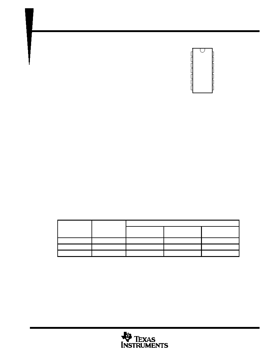
D, J, OR N PACKAGE
(TOP VIEW)
LP239, LP339, LP2901
LOW-POWER QUAD DIFFERENTIAL COMPARATORS
SLCS004A ≠ OCTOBER 1987 ≠ REVISED MAY 1988
2
POST OFFICE BOX 655303
∑
DALLAS, TEXAS 75265
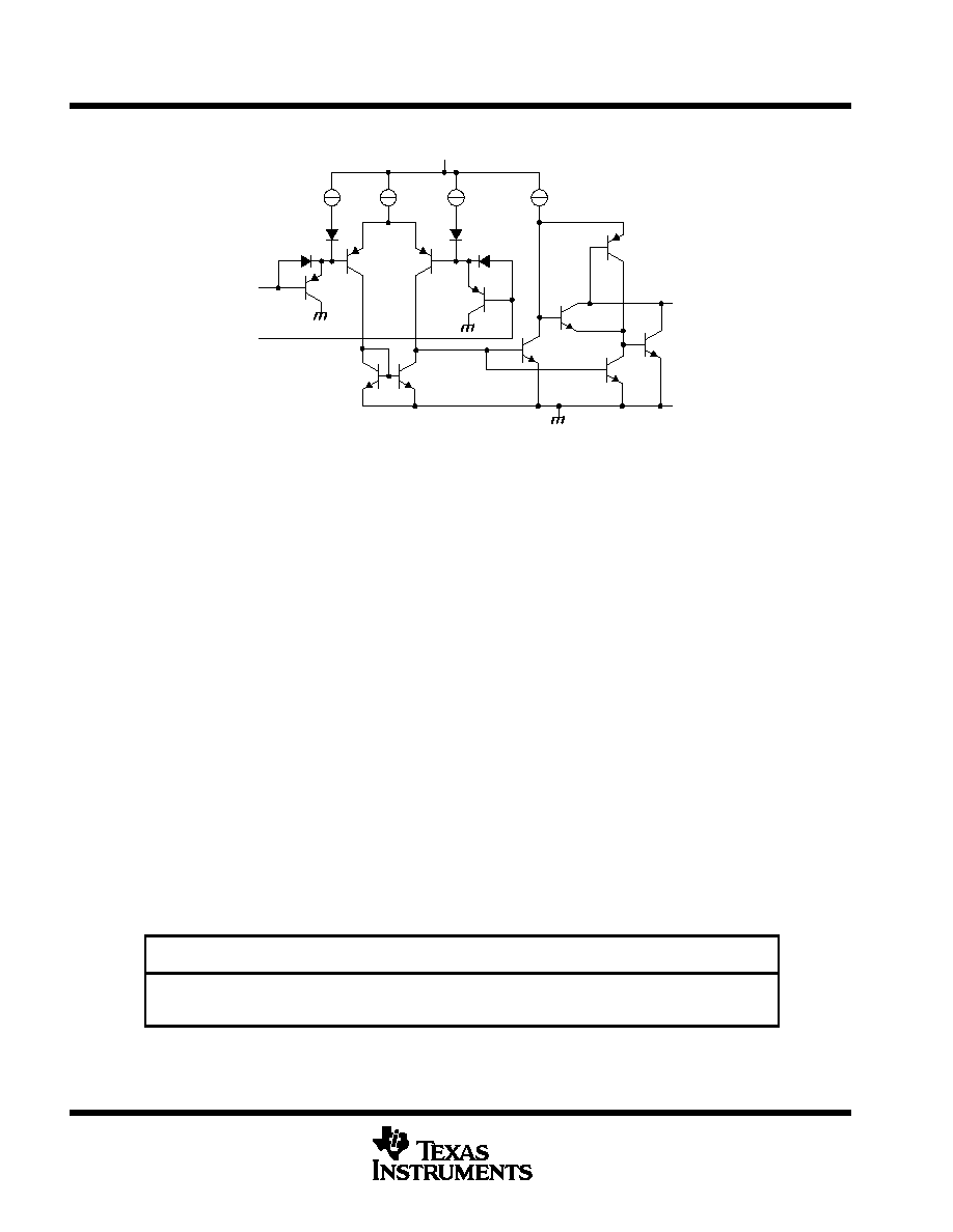
schematic diagram (each comparator)
5
µ
A
IN +
IN ≠
GND
OUT
6
µ
A
0.2
µ
A
VCC
0.2
µ
A
absolute maximum ratings over operating free-air temperature range (unless otherwise noted)
Supply voltage, V
CC
(see Note 1)
36 V
. . . . . . . . . . . . . . . . . . . . . . . . . . . . . . . . . . . . . . . . . . . . . . . . . . . . . . . . . . . .
Differential input voltage, V
ID
(see Note 2)
±
36 V
. . . . . . . . . . . . . . . . . . . . . . . . . . . . . . . . . . . . . . . . . . . . . . . . . . .
Input voltage range, V
I
(either input)
≠ 0.3 V to 36 V
. . . . . . . . . . . . . . . . . . . . . . . . . . . . . . . . . . . . . . . . . . . . . . . . .
Input current, V
I
≠ 0.3 V (see Note 3)
≠ 50 mA
. . . . . . . . . . . . . . . . . . . . . . . . . . . . . . . . . . . . . . . . . . . . . . . . . . . .
Duration of output short-circuit to ground (see Note 4)
Unlimited
. . . . . . . . . . . . . . . . . . . . . . . . . . . . . . . . . . . . . .
Continuous total dissipation (see Note 5)
See Dissipation Rating Table
. . . . . . . . . . . . . . . . . . . . . . . . . . . . . . . .
Operating free-air temperature range, T
A
: LP239 ≠
25
∞
C to 85
∞
C
. . . . . . . . . . . . . . . . . . . . . . . . . . . . . . . . . . . . . .
LP339 0
∞
C to 70
∞
C
. . . . . . . . . . . . . . . . . . . . . . . . . . . . . . . . . . . . . . . .
LP2901 ≠
40
∞
C to 85
∞
C
. . . . . . . . . . . . . . . . . . . . . . . . . . . . . . . . . . . . .
Storage temperature range
≠ 65
∞
C to 150
∞
C
. . . . . . . . . . . . . . . . . . . . . . . . . . . . . . . . . . . . . . . . . . . . . . . . . . . . . . .
Lead temperature range 1,6 mm (1/16 inch) from case for 10 seconds: D or N package
260
∞
C
. . . . . . . . . . .
Lead temperature range 1,6 mm (1/16 inch) from case for 60 seconds: J package
300
∞
C
. . . . . . . . . . . . . . . .
Stresses beyond those listed under absolute maximum ratings may cause permanent damage to the device. These are stress ratings only, and
functional operation of the device at these or any other conditions beyond those indicated in the recommended operating conditions is not implied.
Exposure to absolute-maximum-rated conditions for extended periods may affect device reliability.
NOTES:
1. All voltage values, except differential voltages, are with respect to the network ground.
2. Differential voltages are at IN+ with respect to IN ≠.
3. This input current only exists when the voltage at any of the inputs is driven negative. The current flows through the collector-base
junction of the input clamping device. In addition to the clamping device action, there is lateral n-p-n parasitic transistor action. This
action is not destructive and normal output states are re-established when the input voltage returns to a value more positive than
≠ 0.3 V at TA = 25
∞
C.
4. Short circuits between outputs to VCC can cause excessive heating and eventual destruction.
5. If the output transistors are allowed to saturate, the low bias dissipation and the on-off characteristics of the outputs keep the
dissipation very small (usually less than 100 mW).
DISSIPATION RATING TABLE
PACKAGE
TA
25
∞
C
POWER RATING
DERATING FACTOR
ABOVE TA = 25
∞
C
TA = 70
∞
C
POWER RATING
TA = 85
∞
C
POWER RATING
D
J
N
950 mW
1025 mW
1150 mW
7.6 mW/
∞
C
8.2 mW/
∞
C
9.2 mW/
∞
C
608 mW
656 mW
736 mW
494 mW
533 mW
598 mW
LP239, LP339, LP2901
LOW-POWER QUAD DIFFERENTIAL COMPARATORS
SLCS004A ≠ OCTOBER 1987 ≠ REVISED MAY 1988
3
POST OFFICE BOX 655303
∑
DALLAS, TEXAS 75265
recommended operating conditions
LP239
LP339
LP2901
UNIT
MIN
MAX
MIN
MAX
MIN
MAX
UNIT
VCC
Supply voltage
5
30
5
30
5
30
V
VIC
Common mode input voltage
VCC = 5 V
0
3
0
3
0
3
V
VIC
Common-mode input voltage
VCC = 30 V
0
28
0
28
0
28
V
VI
Input voltage
VCC = 5 V
0
3
0
3
0
3
V
VI
Input voltage
VCC = 30 V
0
28
0
28
0
28
V
TA
Operating free-air temperature
≠ 25
85
0
70
≠ 40
85
∞
C
electrical characteristics, V
CC
= 5 V, T
A
= 25
∞
C
(unless otherwise noted)
PARAMETER
TEST CONDITIONS
TA
MIN
TYP
MAX
UNIT
VIO
Input offset voltage
VCC = 5 V to 30 V,
VO = 2 V,
25
∞
C
±
2
±
5
mV
VIO
Input offset voltage
CC
,
RS = 0,
O
,
See Note 6
Full range
±
9
mV
IIO
Input offset current
25
∞
C
±
0.5
±
5
nA
IIO
Input offset current
Full range
±
1
±
15
nA
IIB
Input bias current
See Note 7
25
∞
C
≠ 2.5
≠ 25
nA
IIB
Input bias current
See Note 7
Full range
≠ 4
≠ 40
nA
VICR
Common-mode input voltage
Single supply
25
∞
C
0 to
VCC ≠ 1.5
V
VICR
g
range
Single supply
Full range
0 to
VCC ≠ 2
V
AVD
Large-signal differential voltage
amplification
VCC = 15 V,
RL = 15 k
500
V/mV
V
1 V
VO = 2 V,
25
∞
C
20
30
Output sink current
VI ≠ = 1 V,
VI + = 0
O
,
See Note 8
Full range
15
mA
VI + = 0
VO = 0.4 V
25
∞
C
0.2
0.7
Output leakage current
VI + = 1 V,
VO = 5 V
25
∞
C
0.1
nA
Output leakage current
I +
,
VI ≠ = 0
VO = 30 V
Full range
1
µ
A
VID
Differential input voltage
VI
0 (or VCC ≠ on split supplies)
36
V
ICC
Supply current
RL =
all comparators
60
100
µ
A
Full range is ≠25
∞
C to 85
∞
C for the LP239, 0
∞
C to 70
∞
C for the LP339, and ≠ 40
∞
C to 85
∞
C for the LP2901.
NOTES:
6. VIO is measured over the full common-mode input voltage range.
7. Because of the p-n-p input stage, the direction of the current is out of the device. This current is essentially constant (i.e., independent
of the output state). No loading change exists on the reference or input lines as long as the common-mode input voltage range is
not exceeded.
8. The output sink current is a function of the output voltage. These devices have a bimodal output section that allows them to sink
(via a Darlington connection) large currents at output voltages greater than 1.5 V, and smaller currents at output voltages
less than 1.5 V.
switching characteristics, V
CC
= 5 V, T
A
= 25
∞
C, R
L
connected to 5 V through 5.1 k
PARAMETER
TEST CONDITIONS
MIN
TYP
MAX
UNIT
Large-signal response time
TTL logic swing V f = 1 4 V
1.3
µ
s
Response time
TTL logic swing, Vref = 1.4 V
8
µ
s
LP239, LP339, LP2901
LOW-POWER QUAD DIFFERENTIAL COMPARATORS
SLCS004A ≠ OCTOBER 1987 ≠ REVISED MAY 1988
4
POST OFFICE BOX 655303
∑
DALLAS, TEXAS 75265
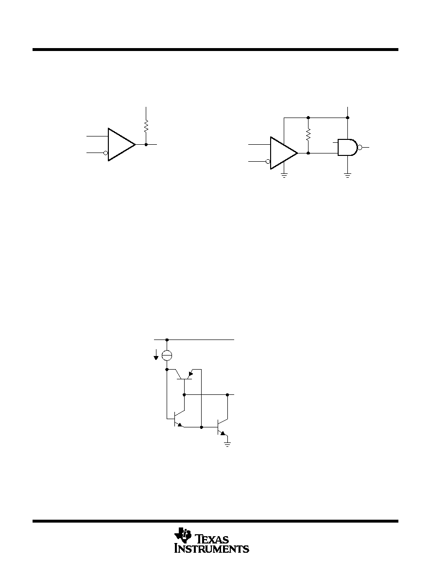
APPLICATION INFORMATION
Figure 1 shows the basic configuration for using the LP239, LP339, or LP2901 comparator. Figure 2 shows the
diagram for using one of these comparators as a CMOS driver.
Figure 1. Basic Comparator
IN +
IN ≠
OUT
30 k
+
≠
VCC
1/4 LP239, LP339,
or LP2901
Figure 2. CMOS Driver
IN +
IN ≠
100 k
1/4 LP239, LP339,
or LP2901
1/4 SN54/74LS00 or
1/4 SN54/74ALS1000A
VCC
+
≠
12
3
OUT
All pins of any unused comparators should be grounded. The bias network of the LP239, LP339, and LP2901
establishes a drain current that is independent of the magnitude of the power supply voltage over the range of
2 V to 30 V. It is usually necessary to use a bypass capacitor across the power supply line.
The differential input voltage may be larger than V
CC
without damaging the device. Protection should be
provided to prevent the input voltages from going negative by more than ≠ 0.3 V. The output section has two
distinct modes of operation: a Darlington mode and a ground-emitter mode. This unique drive circuit permits
the device to sink 30 mA at V
O
= 2 V in the Darlington mode and 700
µ
A at V
O
= 0.4 V in the ground-emitter
mode. Figure 3 is a simplified schematic diagram of the output section. The output section is configured in a
Darlington connection (ignoring Q3). If the output voltage is held high enough (above 1 V), Q1 is not saturated
and the output current is limited only by the product of the h
FE
of Q1, the h
FE
of Q2, and I1 and the 60-
saturation
resistance of Q2. The devices are capable of driving LEDs, relays, etc. in this mode while maintaining an ultralow
power supply current of 60
µ
A typically.
VCC
VO
Q2
Q1
Q3
I1 = 6
µ
A
Figure 3. Output-Section Schematic Diagram

LP239, LP339, LP2901
LOW-POWER QUAD DIFFERENTIAL COMPARATORS
SLCS004A ≠ OCTOBER 1987 ≠ REVISED MAY 1988
5
POST OFFICE BOX 655303
∑
DALLAS, TEXAS 75265
APPLICATION INFORMATION
Without transistor Q3, if the output voltage were allowed to drop below 0.8 V, transistor Q1 would saturate and
the output current would drop to zero. The circuit would be unable to pull low current loads down to ground or
the negative supply, if used. Transistor Q3 has been included to bypass transistor Q1 under these conditions
and apply the current I1 directly to the base of Q2. The output sink current is now approximately I1 times the
h
FE
of Q2 (700
µ
A at V
O
= 0.4 V). The output of the devices exhibit a bimodal characteristic with a smooth
transition between modes.
In both cases, the output is an uncommitted collector. Several outputs can be tied together to provide a dot logic
function. An output pullup resistor can be connected to any available power supply voltage within the permitted
power supply range, and there is no restriction on this voltage based on the magnitude of the voltage that is
supplied to V
CC
of the package.

LP239, LP339, LP2901
LOW-POWER QUAD DIFFERENTIAL COMPARATORS
SLCS004A ≠ OCTOBER 1987 ≠ REVISED MAY 1988
6
POST OFFICE BOX 655303
∑
DALLAS, TEXAS 75265

IMPORTANT NOTICE
Texas Instruments and its subsidiaries (TI) reserve the right to make changes to their products or to discontinue
any product or service without notice, and advise customers to obtain the latest version of relevant information
to verify, before placing orders, that information being relied on is current and complete. All products are sold
subject to the terms and conditions of sale supplied at the time of order acknowledgement, including those
pertaining to warranty, patent infringement, and limitation of liability.
TI warrants performance of its semiconductor products to the specifications applicable at the time of sale in
accordance with TI's standard warranty. Testing and other quality control techniques are utilized to the extent
TI deems necessary to support this warranty. Specific testing of all parameters of each device is not necessarily
performed, except those mandated by government requirements.
CERTAIN APPLICATIONS USING SEMICONDUCTOR PRODUCTS MAY INVOLVE POTENTIAL RISKS OF
DEATH, PERSONAL INJURY, OR SEVERE PROPERTY OR ENVIRONMENTAL DAMAGE ("CRITICAL
APPLICATIONS"). TI SEMICONDUCTOR PRODUCTS ARE NOT DESIGNED, AUTHORIZED, OR
WARRANTED TO BE SUITABLE FOR USE IN LIFE-SUPPORT DEVICES OR SYSTEMS OR OTHER
CRITICAL APPLICATIONS. INCLUSION OF TI PRODUCTS IN SUCH APPLICATIONS IS UNDERSTOOD TO
BE FULLY AT THE CUSTOMER'S RISK.
In order to minimize risks associated with the customer's applications, adequate design and operating
safeguards must be provided by the customer to minimize inherent or procedural hazards.
TI assumes no liability for applications assistance or customer product design. TI does not warrant or represent
that any license, either express or implied, is granted under any patent right, copyright, mask work right, or other
intellectual property right of TI covering or relating to any combination, machine, or process in which such
semiconductor products or services might be or are used. TI's publication of information regarding any third
party's products or services does not constitute TI's approval, warranty or endorsement thereof.
Copyright
©
1998, Texas Instruments Incorporated