 | –≠–ª–µ–∫—Ç—Ä–æ–Ω–Ω—ã–π –∫–æ–º–ø–æ–Ω–µ–Ω—Ç: LP2985LV | –°–∫–∞—á–∞—Ç—å:  PDF PDF  ZIP ZIP |

LP2985LV
150 mA LOW NOISE, LOW DROPOUT REGULATOR
WITH SHUTDOWN FOR OUTPUT VOLTAGES
<
2.3 V
SLVS552 - OCTOBER 2004
1
POST OFFICE BOX 655303
∑
DALLAS, TEXAS 75265
D
Available in the Texas Instruments
NanoStar
and NanoFree
Wafer Chip
Scale Packages
D
Output Tolerance of:
- 1% (A Grade)
- 1.5% (Standard Grade)
D
Ultra Low Dropout, Typically
280 mV at Full Load of 150 mA
D
Wide V
IN
Range . . . 16 V (Max)
D
Low I
Q
. . . 850
µ
A at Full Load at 150 mA
D
Shutdown Current . . . 0.01
µ
A Typ
D
Low Noise . . . 30
µ
V
RMS
With 10-nF Bypass
Capacitor
D
Stable With Low ESR Capacitors, Including
Ceramic
D
Over-Current and Thermal Protection
D
High Peak Current Capability
D
For V
OUT
Options
.
2.5 V, See LP2985 Data
Sheet
D
Portable Applications
- Cellular Phones
- Palmtop and Laptop Computers
- Personal Digital Assistants (PDAs)
- Digital Cameras and Camcorders
- CD Players
- MP3 Players
description/ordering information
The LP2985LV family of fixed-output, low-dropout regulators offers exceptional, cost-effective performance for
both portable and nonportable applications. Available in voltages of 1.25 V, 1.35 V, 1.5 V, 1.7 V, 1.8 V, and
2 V, the family has an output tolerance of 1% for the A version (1.5% for the non-A version), and is capable of
delivering 150-mA continuous load current. Standard regulator features, such as over-current and
over-temperature protection, are included.
The LP2985LV has a host of features that makes the regulator an ideal candidate for a variety of portable
applications:
∑
Low dropout: A PNP pass element allows a typical dropout of 280 mV at 150-mA load current.
∑
Low quiescent current: The use of a vertical PNP process allows for quiescent currents that are
considerably lower than those associated with traditional lateral PNP regulators.
∑
Shutdown: A shutdown feature is available, allowing the regulator to consume only 0.01
µ
A
when the
ON/OFF pin is pulled low.
∑
Low-ESR-capacitor friendly: The regulator is stable with low ESR capacitors, allowing for the use of
small, inexpensive ceramic capacitors in cost-sensitive applications.
Copyright
2004, Texas Instruments Incorporated
DBV (SOT-23) PACKAGE
(TOP VIEW)
1
2
3
5
4
V
IN
GND
ON/OFF
V
OUT
BYPASS
V
OUT
YEQ, YEU, YZQ, OR YZU (WCSP) PACKAGE
(TOP VIEW)
B2
C1
C3
A1
A3
V
IN
BYPASS
ON/OFF
GND
NanoStar and NanoFree are trademarks of Texas Instruments.
Please be aware that an important notice concerning availability, standard warranty, and use in critical applications of
Texas Instruments semiconductor products and disclaimers thereto appears at the end of this data sheet.
PRODUCTION DATA information is current as of publication date.
Products conform to specifications per the terms of Texas Instruments
standard warranty. Production processing does not necessarily include
testing of all parameters.
LP2985LV
150 mA LOW NOISE, LOW DROPOUT REGULATOR
WITH SHUTDOWN FOR OUTPUT VOLTAGES
<
2.3 V
SLVS552 - OCTOBER 2004
2
POST OFFICE BOX 655303
∑
DALLAS, TEXAS 75265
description/ordering information (continued)
∑
Low noise: The BYPASS pin allows for low noise operation, with a typical output noise of 30
µ
V (RMS)
with the use of a 10-nF bypass capacitor.
∑
Small packaging: For the most space-constraint needs, the regulator is available in SOT-23 package,
as well as NanoStar
wafer chip scale packaging, offering an even smaller size with improved thermal
and electrical characteristics. NanoStar package technology is a major breakthrough in IC packaging
concepts, using the die as the package.
PREVIEW
PREVIEW
PREVIEW
PREVIEW
PREVIEW
PREVIEW
PREVIEW
PREVIEW
PREVIEW
PREVIEW
PREVIEW
PREVIEW
PREVIEW
PREVIEW
PREVIEW
PREVIEW
PREVIEW
PREVIEW
PREVIEW
PREVIEW
PREVIEW
PREVIEW
PREVIEW
PREVIEW
PREVIEW
PREVIEW
PREVIEW
PREVIEW
PREVIEW
LP2985LV
150 mA LOW NOISE, LOW DROPOUT REGULATOR
WITH SHUTDOWN FOR OUTPUT VOLTAGES
<
2.3 V
SLVS552 - OCTOBER 2004
3
POST OFFICE BOX 655303
∑
DALLAS, TEXAS 75265
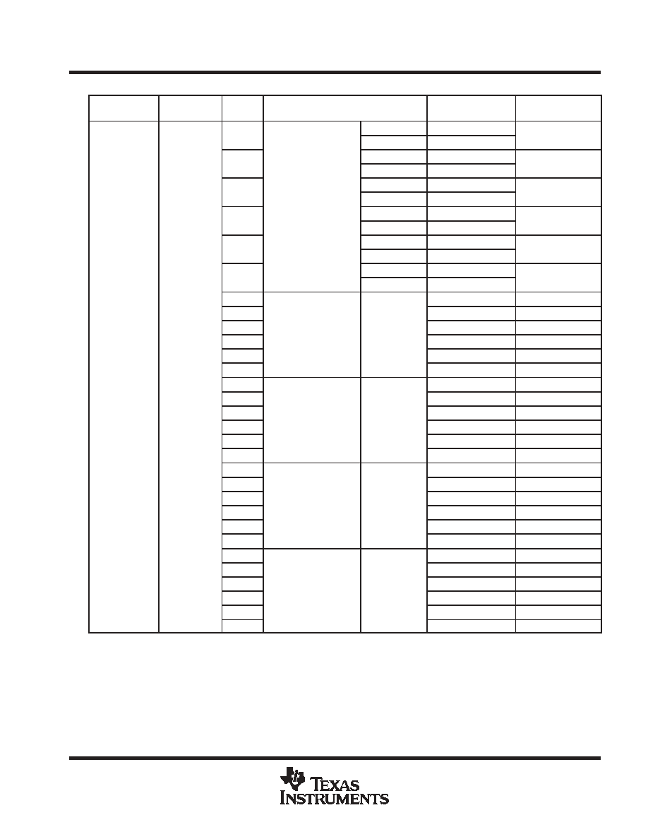
ORDERING INFORMATION
TJ
PART
GRADE
VOUT
(NOM)
PACKAGE
ORDERABLE
PART NUMBER
TOP-SIDE
MARKING
1.25 V
Reel of 3000
LP2985A-12DBVR
1.25 V
Reel of 250
LP2985A-12DBVT
1.35 V
Reel of 3000
LP2985A-13DBVR
1.35 V
Reel of 250
LP2985A-13DBVT
1.5 V
Reel of 3000
LP2985A-15DBVR
1.5 V
SOT23-5 (DBV)
Reel of 250
LP2985A-15DBVT
1.7 V
SOT23-5 (DBV)
Reel of 3000
LP2985A-17DBVR
1.7 V
Reel of 250
LP2985A-17DBVT
1.8 V
Reel of 3000
LP2985A-18DBVR
LPT_
1.8 V
Reel of 250
LP2985A-18DBVT
LPT_
2 V
Reel of 3000
LP2985A-20DBVR
2 V
Reel of 250
LP2985A-20DBVT
1.25 V
LP2985A-12YEQR
1.35 V
LP2985A-13YEQR
1.5 V
NanoStar
- WCSP
Reel of 3000
LP2985A-15YEQR
1.7 V
NanoStar - WCSP
0.17-mm Bump (YEQ)
Reel of 3000
LP2985A-17YEQR
1.8 V
0.17-mm Bump (YEQ)
LP2985A-18YEQR
-40
∞
C to 125
∞
C
A grade:
2 V
LP2985A-20YEQR
-40
∞
C to 125
∞
C
A grade:
1% tolerance
1.25 V
LP2985A-12YZQR
1% tolerance
1.35 V
NanoFree - WCSP
LP2985A-13YZQR
1.5 V
NanoFree
- WCSP
0.17-mm Bump
Reel of 3000
LP2985A-15YZQR
1.7 V
0.17-mm Bump
(YZQ, Pb-free)
Reel of 3000
LP2985A-17YZQR
1.8 V
(YZQ, Pb-free)
LP2985A-18YZQR
2 V
LP2985A-20YZQR
1.25 V
LP2985A-12YEUR
1.35 V
LP2985A-13YEUR
1.5 V
NanoStar
- WCSP
Reel of 3000
LP2985A-15YEUR
1.7 V
NanoStar - WCSP
0.30-mm Bump (YEU)
Reel of 3000
LP2985A-17YEUR
1.8 V
0.30-mm Bump (YEU)
LP2985A-18YEUR
2 V
LP2985A-20YEUR
1.25 V
LP2985A-12YZUR
1.35 V
NanoFree - WCSP
LP2985A-13YZUR
1.5 V
NanoFree
- WCSP
0.30-mm Bump
Reel of 3000
LP2985A-15YZUR
1.7 V
0.30-mm Bump
(YZU, Pb-free)
Reel of 3000
LP2985A-17YZUR
1.8 V
(YZU, Pb-free)
LP2985A-18YZUR
2 V
LP2985A-20YZUR
Package drawings, standard packing quantities, thermal data, symbolization, and PCB design guidelines are available at
www.ti.com/sc/package.
DBV: The actual top-side marking has one additional character that designates the assembly/test site.
YEQ/YZQ, YEU/YZU: The actual top-side marking has three preceding characters to denote year, month, and sequence code, and one
following character to designate the assembly/test site. Pin 1 identifier indicates solder-bump composition (1 = SnPb,
∑
= Pb-free).

PREVIEW
PREVIEW
PREVIEW
PREVIEW
PREVIEW
PREVIEW
PREVIEW
PREVIEW
PREVIEW
PREVIEW
PREVIEW
PREVIEW
PREVIEW
PREVIEW
PREVIEW
PREVIEW
PREVIEW
PREVIEW
PREVIEW
PREVIEW
PREVIEW
PREVIEW
PREVIEW
PREVIEW
PREVIEW
PREVIEW
PREVIEW
PREVIEW
PREVIEW
LP2985LV
150 mA LOW NOISE, LOW DROPOUT REGULATOR
WITH SHUTDOWN FOR OUTPUT VOLTAGES
<
2.3 V
SLVS552 - OCTOBER 2004
4
POST OFFICE BOX 655303
∑
DALLAS, TEXAS 75265
description/ordering information (continued)
ORDERING INFORMATION
TJ
PART GRADE
VOUT
(NOM)
PACKAGE
ORDERABLE
PART NUMBER
TOP-SIDE
MARKING
1.25 V
Reel of 3000
LP2985-12DBVR
1.25 V
Reel of 250
LP2985-12DBVT
1.35 V
Reel of 3000
LP2985-13DBVR
1.35 V
Reel of 250
LP2985-13DBVT
1.5 V
Reel of 3000
LP2985-15DBVR
1.5 V
SOT-23 (DBV)
Reel of 250
LP2985-15DBVT
1.7 V
SOT-23 (DBV)
Reel of 3000
LP2985-17DBVR
1.7 V
Reel of 250
LP2985-17DBVT
1.8 V
Reel of 3000
LP2985-18DBVR
LPH_
1.8 V
Reel of 250
LP2985-18DBVT
LPH_
2 V
Reel of 3000
LP2985-20DBVR
2 V
Reel of 250
LP2985-20DBVT
1.25 V
LP2985-12YEQR
1.35 V
LP2985-13YEQR
1.5 V
NanoStar
- WCSP
Reel of 3000
LP2985-15YEQR
1.7 V
NanoStar - WCSP
0.17-mm Bump (YEQ)
Reel of 3000
LP2985-17YEQR
1.8 V
0.17-mm Bump (YEQ)
LP2985-18YEQR
-40
∞
C to 125
∞
C
Standard grade:
2 V
LP2985-20YEQR
-40
∞
C to 125
∞
C
Standard grade:
1.5% tolerance
1.25 V
LP2985-12YZQR
1.5% tolerance
1.35 V
NanoFree - WCSP
LP2985-13YZQR
1.5 V
NanoFree
- WCSP
0.17-mm Bump
Reel of 3000
LP2985-15YZQR
1.7 V
0.17-mm Bump
(YZQ, Pb free)
Reel of 3000
LP2985-17YZQR
1.8 V
(YZQ, Pb free)
LP2985-18YZQR
2 V
LP2985-20YZQR
1.25 V
LP2985-12YEUR
1.35 V
LP2985-13YEUR
1.5 V
NanoStar
- WCSP
Reel of 3000
LP2985-15YEUR
1.7 V
NanoStar - WCSP
0.30-mm Bump (YEU)
Reel of 3000
LP2985-17YEUR
1.8 V
0.30-mm Bump (YEU)
LP2985-18YEUR
2 V
LP2985-20YEUR
1.25 V
LP2985-12YZUR
1.35 V
NanoFree - WCSP
LP2985-13YZUR
1.5 V
NanoFree
- WCSP
0.30-mm Bump
Reel of 3000
LP2985-15YZUR
1.7 V
0.30-mm Bump
(YZQ, Pb free)
Reel of 3000
LP2985-17YZUR
1.8 V
(YZQ, Pb free)
LP2985-18YZUR
2 V
LP2985-20YZUR
Package drawings, standard packing quantities, thermal data, symbolization, and PCB design guidelines are available at
www.ti.com/sc/package.
DBV: The actual top-side marking has one additional character that designates the assembly/test site.
YEQ/YZQ, YEU/YZU: The actual top-side marking has three preceding characters to denote year, month, and sequence code, and one
following character to designate the assembly/test site. Pin 1 identifier indicates solder-bump composition
(1 = SnPb,
∑
= Pb-free).
LP2985LV
150 mA LOW NOISE, LOW DROPOUT REGULATOR
WITH SHUTDOWN FOR OUTPUT VOLTAGES
<
2.3 V
SLVS552 - OCTOBER 2004
5
POST OFFICE BOX 655303
∑
DALLAS, TEXAS 75265
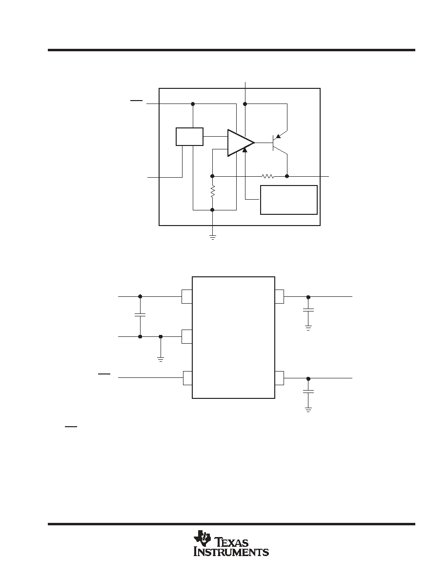
functional block diagram
VIN
VOUT
ON/OFF
Over-Current/
Over-Temperature
Protection
VREF
1.23 V
-
+
BYPASS
basic application circuit
VOUT
2.2
µ
F
10 nF
w
1
µ
F
VIN
1
ON/OFF
}
Minimum COUT value for stability (can be increased without limit for improved stability and transient response)
ON/OFF must be actively terminated. Connect to VIN if shutdown feature is not used.
ß Optional BYPASS capacitor for low noise operation
2
GND
3
5
4
BYPASS
LP2985A-xxDBVR