 | –≠–ª–µ–∫—Ç—Ä–æ–Ω–Ω—ã–π –∫–æ–º–ø–æ–Ω–µ–Ω—Ç: LT1007AC | –°–∫–∞—á–∞—Ç—å:  PDF PDF  ZIP ZIP |
LT1007, LT1007A, LT1037, LT1037A
LOW-NOISE, HIGH-SPEED, PRECISION OPERATIONAL AMPLIFIERS
SLOS017C ≠ D3195, FEBRUARY 1989 ≠ REVISED JANUARY 1993
POST OFFICE BOX 655303
∑
DALLAS, TEXAS 75265
Copyright
©
1993, Texas Instruments Incorporated
1
∑
Maximum Equivalent Input Noise Voltage:
3.8 nV/
Hz at 1 kHz
4.5 nV/
Hz at 10 Hz
∑
Low Peak-to-Peak Equivalent Input Noise
Voltage: 60 nV Typ From 0.1 Hz to 10 Hz
∑
Slew Rate (LT1037 and LT1037A):
11 V/
µ
s Min
LT1007A and LT1037A Specifications:
∑
High Voltage Amplification:
7 V/
µ
V Min, R
L
= 2 k
3 V/
µ
V Min, R
L
= 600
∑
Low Input Offset Voltage:
25
µ
V Max
∑
Low Input Offset Voltage Temperature
Coefficient: 0.6
µ
V/
∞
C Max
∑
Common-Mode Rejection Ratio: 117 dB Min
description
These monolithic operational amplifiers feature
extremely low-noise performance and out
standing precision and speed specifications.The typical differential voltage amplification (at T
A
= 25
∞
C) of these
devices is an extremely high 20 V/
µ
V driving a 2-k
load to
±
1
2 V and 12 V/
µ
V driving, a 600 -
load to
±
10V.
In the design, processing, and testing of the device, particular attention has been paid to the optimization of the
entire distribution of several key parameters. Consequently, the specifications of even the lowest-cost grades
(the LT1007C and the LT1037C) have been greatly improved compared to equivalent grades of competing
amplifiers.
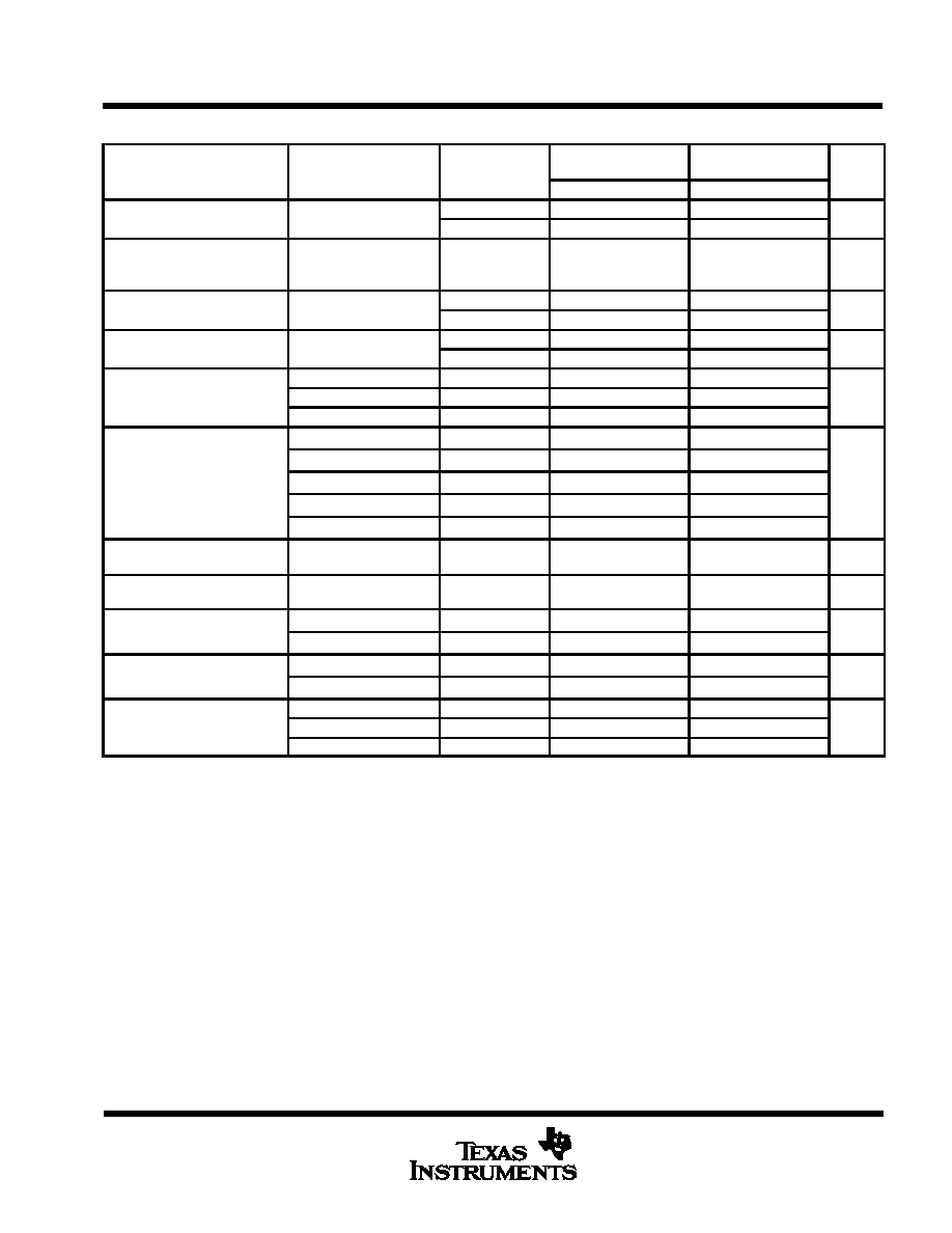
AVAILABLE OPTIONS
VIO max
PACKAGE
TA
VIO max
AT 25
∞
C
SMALL-OUTLINE
(DW)
CERAMIC DIP
(JG)
PLASTIC DIP
(P)
60
µ
V
LT1007CDW
--
LT1007CP
0
∞
C
to
25
µ
V
--
--
LT1007ACP
to
70
∞
C
60
µ
V
LT1037CDW
--
LT1037CP
70 C
25
µ
V
--
--
LT1037ACP
C
60
µ
V
--
LT1007MJG
LT1007MP
≠ 55
∞
C
to
25
µ
V
--
LT1007AMJG
LT1007AMP
to
125
∞
C
60
µ
V
--
LT1037MJG
LT1037MP
125 C
25
µ
V
--
LT1037AMJG
LT1037AMP
The DW packages are available taped and reeled. Add the suffix R to the device type,
(e.g.,LT1007CDWR).
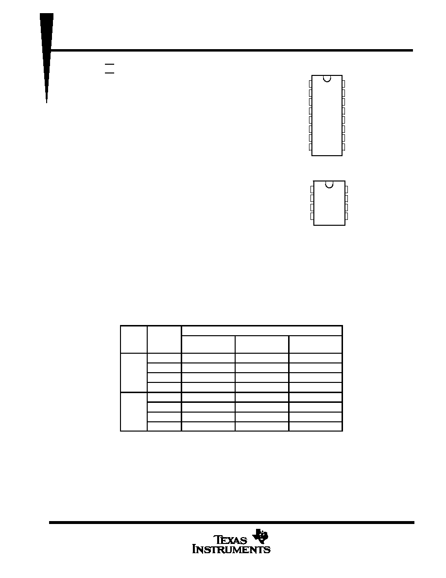
1
2
3
4
5
6
7
8
16
15
14
13
12
11
10
9
NC
NC
V
IO
TRIM
IN ≠
IN +
V
CC ≠
NC
NC
NC
NC
V
IO
TRIM
V
CC+
OUT
NC
NC
NC
(TOP VIEW)
DW PACKAGE
1
2
3
4
8
7
6
5
V
IO
TRIM
IN ≠
IN +
V
CC ≠
V
IO
TRIM
V
CC +
OUT
NC
JG OR P PACKAGE
(TOP VIEW)
NC ≠ No internal connection
PRODUCTION DATA information is current as of publication date.
Products conform to specifications per the terms of Texas Instruments
standard warranty. Production processing does not necessarily include
testing of all parameters.
L
T1007, L
T1007A, L
T1037, L
T1037A
LOW
-NOISE, HIGH-SPEED, PRECISION OPERA
TIONAL
AMPLIFIERS
SLOS017C ≠ D3195, FEBRUAR
Y 1989 ≠ REVISED JANUAR
Y 1993
2
POST
OFFICE BOX 655303 DALLAS,
TEXAS
75265
∑
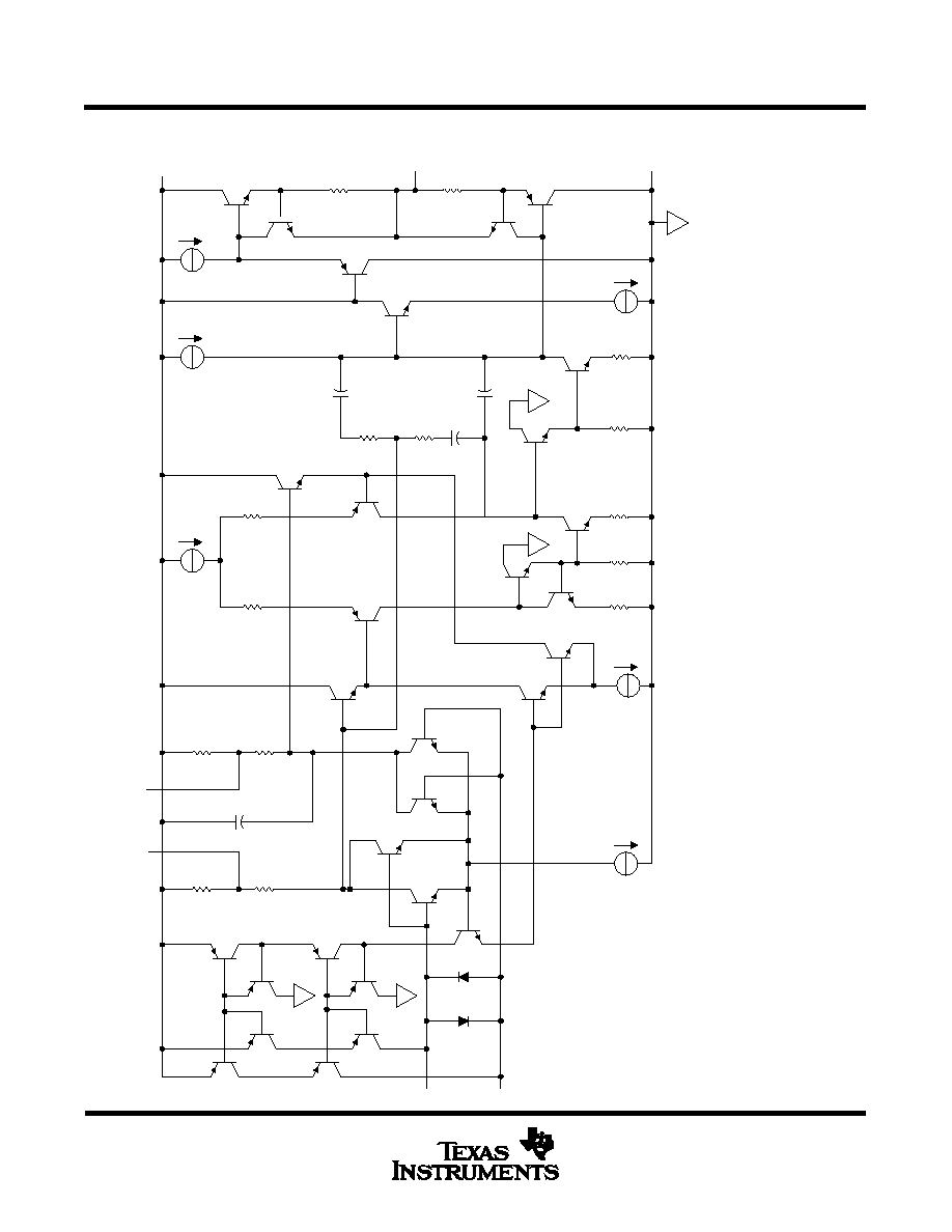
schematic
TRIM
TRIM
Q29
OUT
Q28
Q30
Q27
Q26
Q25
20 pF
80 pF
C1
Q18
450 A
130 pF
IN ≠
IN +
Q5
Q3
Q6
Q4
Q7
Q8
Q10
Q9
Q13
Q1A
Q1B
Q2B
Q11
Q20
Q19
Q17
Q2A
Q12 Q15
Q24
Q16
Q22
Q23
C1 = 110 pF for LT1007
C1 = 12 pF for LT1037
All component values shown are nominal.
≠
≠
≠
≠
≠
240
µ
A
120
µ
A
VIO
VIO
3.4 k
17 k
3.4 k
17 k
1.2 k
1.2 k
750
µ
A
240
µ
A
VCC +
VCC ≠
20
20
50
6 k
200
6 k
200
200
750
500
µ
A
LT1007, LT1007A, LT1037, LT1037A
LOW-NOISE, HIGH-SPEED, PRECISION OPERATIONAL AMPLIFIERS
SLOS017C ≠ D3195, FEBRUARY 1989 ≠ REVISED JANUARY 1993
POST OFFICE BOX 655303
∑
DALLAS, TEXAS 75265
3
absolute maximum ratings over operating free-air temperature range (unless otherwise noted)
Supply voltage, V
CC +
(see Note 1)
22 V
. . . . . . . . . . . . . . . . . . . . . . . . . . . . . . . . . . . . . . . . . . . . . . . . . . . . . . . . . .
Supply voltage, V
CC ≠
≠ 22 V
. . . . . . . . . . . . . . . . . . . . . . . . . . . . . . . . . . . . . . . . . . . . . . . . . . . . . . . . . . . . . . . . . . . .
Input voltage
V
CC
±
. . . . . . . . . . . . . . . . . . . . . . . . . . . . . . . . . . . . . . . . . . . . . . . . . . . . . . . . . . . . . . . . . . . . . . . . . . . .
Duration of output short circuit
Unlimited
. . . . . . . . . . . . . . . . . . . . . . . . . . . . . . . . . . . . . . . . . . . . . . . . . . . . . . . . . .
Differential input current (see Note 2)
±
25 mA
. . . . . . . . . . . . . . . . . . . . . . . . . . . . . . . . . . . . . . . . . . . . . . . . . . . . .
Power dissipation
See Dissipation Rating Table
. . . . . . . . . . . . . . . . . . . . . . . . . . . . . . . . . . . . . . . . . . . . . . . . . . . .
Operating free-air temperature range:
LT1007C, LT1007AC, LT1037C, LT1037AC
0
∞
C to 70
∞
C
. . . . . . . . . . . . . . . . . . . . . . . . . . . . . . . . . . . . . . .
LT1007M, LT1007AM, LT1037M, LT1037AM
≠ 55
∞
C to 125
∞
C
. . . . . . . . . . . . . . . . . . . . . . . . . . . . . . . . . . .
Storage temperature range
≠ 65
∞
C to 150
∞
C
. . . . . . . . . . . . . . . . . . . . . . . . . . . . . . . . . . . . . . . . . . . . . . . . . . . . . . .
Lead temperature 1,6 mm (1/16 inch) from case for 10 seconds: DW and P packages
260
∞
C
. . . . . . . . . . . .
Lead temperature 1,6 mm (1/16 inch) from case for 60 seconds: JG package
300
∞
C
. . . . . . . . . . . . . . . . . . . .
NOTES: 1. All voltage values, unless otherwise noted, are with respect to the midpoint between VCC + and VCC ≠.
2. The inputs are protected by back-to-back diodes. Current limiting resistors are not used in order to achieve low noise. Excessive input
current will flow if a differential input voltage in excess of approximately
±
0.7 V is applied between the inputs, unless some limiting
resistance is used.
DISSIPATION RATING TABLE
PACKAGE
TA
25
∞
C
POWER RATING
DERATING FACTOR
ABOVE TA = 25
∞
C
TA = 70
∞
C
POWER RATING
TA = 125
∞
C
POWER RATING
DW
1025 mW
8.2 mW/
∞
C
656 mW
N/A
JG
1050 mW
8.4 mW/
∞
C
672 mW
210 mW
P
1000 mW
8 mW/
∞
C
640 mW
200 mW
recommended operating conditions
C-SUFFIX
M-SUFFIX
UNIT
MIN
NOM
MAX
MIN
NOM
MAX
UNIT
Supply voltage, VCC +
4
15
22
4
15
22
V
Supply voltage, VCC ≠
≠ 4
≠ 15
≠ 22
≠ 4
≠ 15
≠ 22
V
Input voltage VI
TA = 25
∞
C
±
11
±
11
V
Input voltage, VI
TA = full range
±
10.5
±
10.3
V
Operating free-air temperature, TA
0
70
≠ 55
125
∞
C
LT1007, LT1007A, LT1037, LT1037A
LOW-NOISE, HIGH-SPEED, PRECISION OPERATIONAL AMPLIFIERS
SLOS017C ≠ D3195, FEBRUARY 1989 ≠ REVISED JANUARY 1993
POST OFFICE BOX 655303
∑
DALLAS, TEXAS 75265
4
electrical characteristics, V
CC
±
=
±
15 V
PARAMETER
TEST CONDITIONS
TA
LT1007C, LT1037C
LT1007AC, LT1037AC
UNIT
PARAMETER
TEST CONDITIONS
TA
MIN
TYP
MAX
MIN
TYP
MAX
UNIT
VIO
Input offset voltage
See Note 3
25
∞
C
20
60
10
25
µ
V
VIO
Input offset voltage
See Note 3
0
∞
C to 70
∞
C
110
50
µ
V
VIO
Average temperature
coefficient of input
offset voltage
0
∞
C to 70
∞
C
1
0.6
µ
V/
∞
C
IIO
Input offset current
25
∞
C
12
50
7
30
nA
IIO
Input offset current
0
∞
C to 70
∞
C
70
40
nA
IIB
Input bias current
25
∞
C
±
15
±
55
±
10
±
35
nA
IIB
Input bias current
0
∞
C to 70
∞
C
±
75
±
45
nA
Peak output voltage
RL= 2 k
25
∞
C
±
12.5
±
13.5
±
13
±
13.8
VOM
Peak output voltage
swing
RL= 600
25
∞
C
±
10.5
±
12.5
±
11
±
12.5
V
swing
RL= 2 k
0
∞
C to 70
∞
C
±
12
±
12.5
RL
2 k
,
VO =
±
12 V
25
∞
C
5
20
7
20
Large-signal
RL
1
,
VO =
±
10 V
25
∞
C
3.5
16
5
16
AVD
Large signal
differential voltage
lifi
i
RL
600
,
VO =
±
10 V
25
∞
C
2
12
3
12
V
/µ
V
amplification
RL
2 k
,
VO =
±
10 V
0
∞
C to 70
∞
C
2.5
4
RL
1 k
,
VO =
±
10 V
0
∞
C to 70
∞
C
2
2.5
ri(CM)
Common-mode input
resistance
25
∞
C
5
7
G
ro
Open-loop output
resistance
25
∞
C
70
70
CMRR
Common-mode
VIC =
±
11 V
25
∞
C
110
126
117
130
dB
CMRR
rejection ratio
VIC =
±
10.5 V
0
∞
C to 70
∞
C
106
114
dB
kSVR
Supply voltage
VCC
±
=
±
4 V to
±
18 V
25
∞
C
106
126
110
130
dB
kSVR
rejection ratio
VCC
±
=
±
4.5 V to
±
18 V
0
∞
C to 70
∞
C
102
106
dB
LT1007C, LT1007AC
25
∞
C
80
140
80
120
PD
Power dissipation
LT1037C, LT1037AC
25
∞
C
85
140
80
130
mW
0
∞
C to 70
∞
C
160
144
NOTE 3: VIO measurements are performed by automatic test equipment approximately 0.5 seconds after application of power.
LT1007, LT1007A, LT1037, LT1037A
LOW-NOISE, HIGH-SPEED, PRECISION OPERATIONAL AMPLIFIERS
SLOS017C ≠ D3195, FEBRUARY 1989 ≠ REVISED JANUARY 1993
POST OFFICE BOX 655303
∑
DALLAS, TEXAS 75265
5
electrical characteristics, V
CC
±
=
±
15 V
PARAMETER
TEST CONDITIONS
TA
LT1007M,
LT1037M
LT1007AM,
LT1037AM
UNIT
A
MIN
TYP
MAX
MIN
TYP
MAX
VIO
Input offset voltage
See Note 3
25
∞
C
20
60
10
25
µ
V
VIO
Input offset voltage
See Note 3
≠ 55
∞
C to 125
∞
C
160
60
µ
V
VIO
Average temperature
coefficient of input
offset voltage
≠ 55
∞
C to 125
∞
C
1
0.6
µ
V/
∞
C
IIO
Input offset current
25
∞
C
12
50
7
30
nA
IIO
Input offset current
≠ 55
∞
C to 125
∞
C
85
50
nA
IIB
Input bias current
25
∞
C
±
15
±
55
±
10
±
35
nA
IIB
Input bias current
≠ 55
∞
C to 125
∞
C
±
95
±
60
nA
Peak output voltage
RL = 2 k
25
∞
C
±
12.5
±
13.5
±
13
±
13.8
VOM
Peak output voltage
swing
RL = 600
25
∞
C
±
10.5
±
12.5
±
11
±
12.5
V
swing
RL = 2 k
≠ 55
∞
C to 125
∞
C
±
12
±
12.5
RL
2 k
,
VO =
±
12 V
25
∞
C
5
20
7
20
Large-signal
RL
1 k
,
VO =
±
10 V
25
∞
C
3.5
16
5
16
AVD
Large signal
differential voltage
lifi
i
RL
600
,
VO =
±
10 V
25
∞
C
2
12
3
12
V
/µ
V
amplification
RL
2 k
,
VO =
±
10 V
≠ 55
∞
C to 125
∞
C
2
3
RL
1 k
,
VO =
±
10 V
≠ 55
∞
C to 125
∞
C
1.5
2
ri(CM)
Common-mode input
resistance
25
∞
C
5
7
G
ro
Open-loop output
resistance
25
∞
C
70
70
CMRR
Common-mode
VIC =
±
11 V
25
∞
C
110
126
117
130
dB
CMRR
rejection ratio
VIC =
±
10.3 V
≠ 55
∞
C to 125
∞
C
104
112
dB
kSVR
Supply voltage
VCC
±
=
±
4 V to
±
18 V
25
∞
C
106
126
110
130
dB
kSVR
y
g
rejection ratio
VCC
±
=
±
4
.
5 V to
±
18 V
≠ 55
∞
C to 125
∞
C
100
104
dB
LT1007M, LT1007AM
25
∞
C
80
140
80
120
PD
Power dissipation
LT1037M, LT1037AM
25
∞
C
85
140
80
130
mW
≠ 55
∞
C to 125
∞
C
170
150
NOTE 3: VIO measurements are performed by automatic test equipment approximately 0.5 seconds after application of power.