LT1054
SWITCHED CAPACITOR VOLTAGE CONVERTERS
WITH REGULATORS
SLVS033F - FEBRUARY 1990 - REVISED NOVEMBER 2004
1
POST OFFICE BOX 655303
∑
DALLAS, TEXAS 75265
D
Output Current . . . 100 mA
D
Low Loss . . . 1.1 V at 100 mA
D
Operating Range . . . 3.5 V to 15 V
D
Reference and Error Amplifier for
Regulation
D
External Shutdown
D
External Oscillator Synchronization
D
Devices Can Be Paralleled
D
Pin-to-Pin Compatible With the
LTC1044/7660
description/ordering information
The LT1054 is a bipolar, switched-capacitor
voltage converter with regulator. It provides higher
output current and significantly lower voltage
losses than previously available converters. An
adaptive-switch drive scheme optimizes
efficiency over a wide range of output currents.
Total voltage drop at 100-mA output current
typically is 1.1 V. This applies to the full
supply-voltage range of 3.5 V to 15 V. Quiescent
current typically is 2.5 mA.
The LT1054 also provides regulation, a feature previously not available in switched-capacitor voltage
converters. By adding an external resistive divider, a regulated output can be obtained. This output is regulated
against changes in both input voltage and output current. The LT1054 also can be shut down by grounding the
feedback terminal. Supply current in shutdown typically is 100
µ
A.
The internal oscillator of the LT1054 runs at a nominal frequency of 25 kHz. The oscillator terminal can be used
to adjust the switching frequency or to externally synchronize the LT1054.
The LT1054C is characterized for operation over a free-air temperature range of 0
∞
C to 70
∞
C. The LT1054I is
characterized for operation over a free-air temperature range of -40
∞
C to 85
∞
C.
ORDERING INFORMATION
TA
PACKAGE
ORDERABLE
PART NUMBER
TOP-SIDE
MARKING
PDIP (P)
Tube of 50
LT1054IP
LT1054IP
-40
∞
C to 85
∞
C
SOIC (DW)
Tube of 40
LT1054IDW
LT1054I
-40 C to 85 C
SOIC (DW)
Reel of 2000
LT1054IDWR
LT1054I
PDIP (P)
Tube of 50
LT1054CP
LT1054CP
0
∞
C to 70
∞
C
SOIC (DW)
Tube of 40
LT1054CDW
LT1054C
0 C to 70 C
SOIC (DW)
Reel of 2000
LT1054CDWR
LT1054C
Package drawings, standard packing quantities, thermal data, symbolization, and PCB design guidelines are
available at www.ti.com/sc/package.
Copyright
2004, Texas Instruments Incorporated
PRODUCTION DATA information is current as of publication date.
Products conform to specifications per the terms of Texas Instruments
standard warranty. Production processing does not necessarily include
testing of all parameters.
DW PACKAGE
(TOP VIEW)
P PACKAGE
(TOP VIEW)
1
2
3
4
8
7
6
5
FB/SD
CAP+
GND
CAP-
V
CC
OSC
V
REF
V
OUT
1
2
3
4
5
6
7
8
16
15
14
13
12
11
10
9
NC
NC
FB/SD
CAP+
GND
CAP-
NC
NC
NC
NC
V
CC
OSC
V
REF
V
OUT
NC
NC
NC - No internal connection
LT1054
SWITCHED CAPACITOR VOLTAGE CONVERTERS
WITH REGULATORS
SLVS033F - FEBRUARY 1990 - REVISED NOVEMBER 2004
2
POST OFFICE BOX 655303
∑
DALLAS, TEXAS 75265
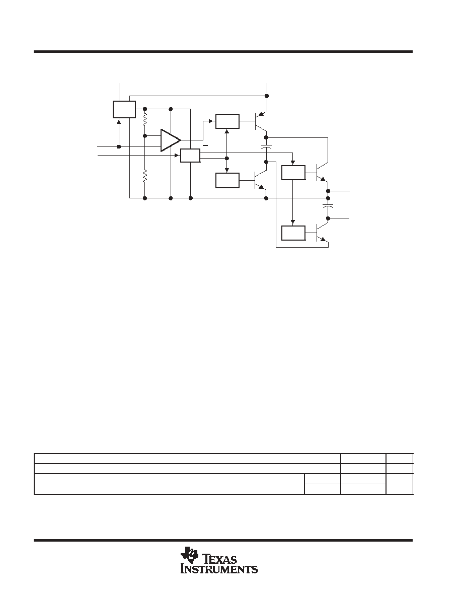
functional block diagram
VREF
Ref
+
-
OSC
Q
Q
Drive
CAP +
VCC
GND
VOUT
FB/SD
OSC
2.5 V
CAP -
COUT
CIN
External capacitors
Pin numbers shown are for the P package.
Drive
Drive
Drive
R
R
1
7
3
5
2
4
8
6
absolute maximum ratings over operating free-air temperature range (unless otherwise noted)
Supply voltage, V
CC
(see Note 1)
16 V
. . . . . . . . . . . . . . . . . . . . . . . . . . . . . . . . . . . . . . . . . . . . . . . . . . . . . . . . . . .
Input voltage range, V
I
: FB/SD
0 V to V
CC
. . . . . . . . . . . . . . . . . . . . . . . . . . . . . . . . . . . . . . . . . . . . . . . . . . . . . . . .
OSC
0 V to V
ref
. . . . . . . . . . . . . . . . . . . . . . . . . . . . . . . . . . . . . . . . . . . . . . . . . . . . . . . . . . .
Junction temperature, T
J
(see Note 2): LT1054C
125
∞
C
. . . . . . . . . . . . . . . . . . . . . . . . . . . . . . . . . . . . . . . . . . . . .
LT1054I 135
∞
C
. . . . . . . . . . . . . . . . . . . . . . . . . . . . . . . . . . . . . . . . . . . . . .
Package thermal impedance,
JA
(see Notes 3 and 4): DW package
57
∞
C/W
. . . . . . . . . . . . . . . . . . . . . . . . . .
P package
85
∞
C/W
. . . . . . . . . . . . . . . . . . . . . . . . . . . .
Storage temperature range, T
stg
-55
∞
C to 150
∞
C
. . . . . . . . . . . . . . . . . . . . . . . . . . . . . . . . . . . . . . . . . . . . . . . . . . .
Stresses beyond those listed under "absolute maximum ratings" may cause permanent damage to the device. These are stress ratings only, and
functional operation of the device at these or any other conditions beyond those indicated under "recommended operating conditions" is not
implied. Exposure to absolute-maximum-rated conditions for extended periods may affect device reliability.
NOTES:
1. The absolute maximum supply-voltage rating of 16 V is for unregulated circuits. For regulation-mode circuits with VOUT
15 V, this
rating may be increased to 20 V.
2. The devices are functional up to the absolute maximum junction temperature.
3. Maximum power dissipation is a function of TJ(max),
JA, and TA. The maximum allowable power dissipation at any allowable
ambient temperature is PD = (TJ(max) - TA)/
JA. Operating at the absolute maximum TJ of 150
∞
C can impact reliability.
4. The package thermal impedance is calculated in accordance with JESD 51-7.
recommended operating conditions
MIN
MAX
UNIT
VCC
Supply voltage
3.5
15
V
TA
Operating free-air temperature range
LT1054C
0
70
∞
C
TA
Operating free-air temperature range
LT1054I
-40
85
∞
C
LT1054
SWITCHED CAPACITOR VOLTAGE CONVERTERS
WITH REGULATORS
SLVS033F - FEBRUARY 1990 - REVISED NOVEMBER 2004
3
POST OFFICE BOX 655303
∑
DALLAS, TEXAS 75265
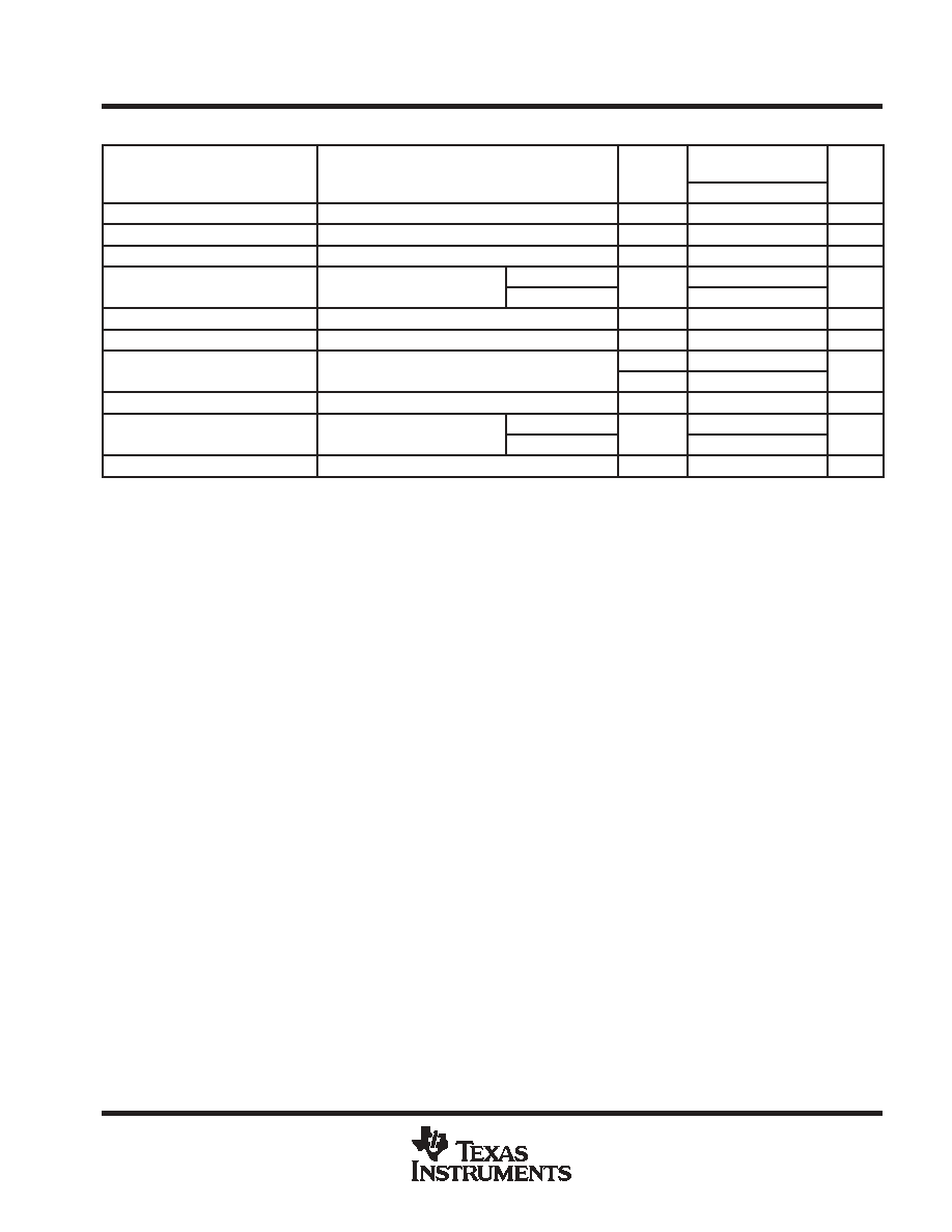
electrical characteristics over recommended operating conditions (unless otherwise noted)
PARAMETER
TEST CONDITIONS
TA
LT1054C
LT1054I
UNIT
PARAMETER
TEST CONDITIONS
TA
MIN
TYP
MAX
UNIT
VO
Regulated output voltage
VCC = 7 V, TJ = 25
∞
C, RL = 500
, See Note 5
25
∞
C
-4.7
-5
-5.2
V
Input regulation
VCC = 7 V to 12 V, RL = 500
, See Note 5
Full range
5
25
mV
Output regulation
VCC = 7 V, RL = 100
to 500
, See Note 5
Full range
10
50
mV
Voltage loss,
CI = CO = 100- F tantalum
IO = 10 mA
Full range
0.35
0.55
V
Voltage loss,
VCC - |VO
(see Note 6)
CI = CO = 100-
µ
F tantalum
IO = 100 mA
Full range
1.1
1.6
V
Output resistance
IO = 10 mA to 100 mA,
See Note 7
Full range
10
15
Oscillator frequency
VCC = 3.5 V to 15 V
Full range
15
25
35
kHz
Vref
Reference voltage
I(REF) = 60 A
25
∞
C
2.35
2.5
2.65
V
Vref
Reference voltage
I(REF) = 60
µ
A
Full range
2.25
2.75
V
Maximum switch current
25
∞
C
300
mA
ICC
Supply current
IO = 0
VCC = 3.5 V
Full range
2.5
4
mA
ICC
Supply current
IO = 0
VCC = 15 V
Full range
3
5
mA
Supply current in shutdown
V(FB/SD) = 0 V
Full range
100
200
µ
A
Full range is 0
∞
C to 70
∞
C for the LT1054C and -40
∞
C to 85
∞
C for the LT1054I.
All typical values are at TA = 25
∞
C.
NOTES:
5. All regulation specifications are for a device connected as a positive-to-negative converter/regulator with R1 = 20 k
, R2 = 102.5 k
,
external capacitor CIN = 10
µ
F (tantalum), external capacitor COUT = 100
µ
F (tantalum) and C1 = 0.002
µ
F (see Figure 15).
6. For voltage-loss tests, the device is connected as a voltage inverter, with terminals 1, 6, and 7 unconnected. The voltage losses
may be higher in other configurations. CIN and COUT are external capacitors.
7. Output resistance is defined as the slope of the curve (
VO versus
IO) for output currents of 10 mA to 100 mA. This represents
the linear portion of the curve. The incremental slope of the curve is higher at currents less than 10 mA due to the characteristics
of the switch transistors.
LT1054
SWITCHED CAPACITOR VOLTAGE CONVERTERS
WITH REGULATORS
SLVS033F - FEBRUARY 1990 - REVISED NOVEMBER 2004
4
POST OFFICE BOX 655303
∑
DALLAS, TEXAS 75265
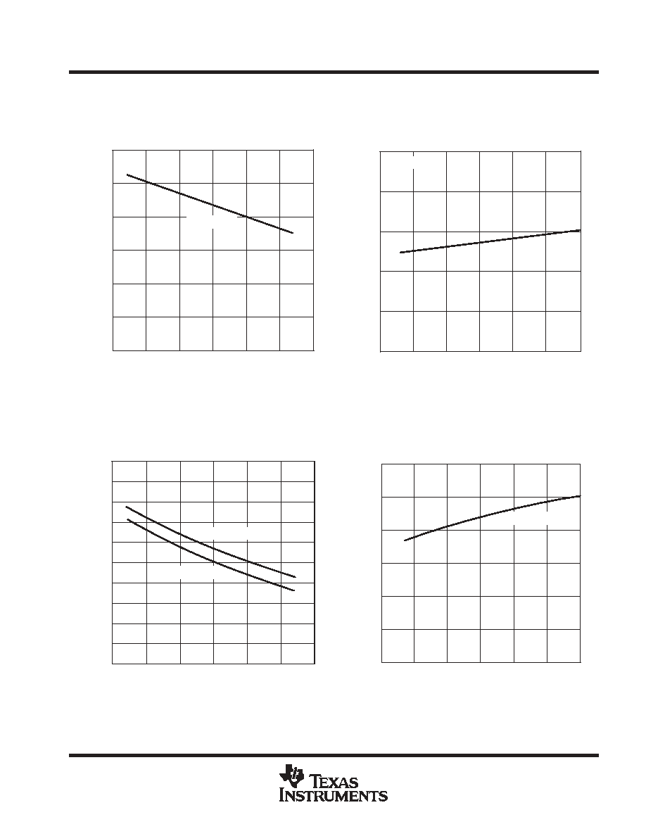
TYPICAL CHARACTERISTICS
Table of Graphs
FIGURE
Shutdown threshold voltage vs Free-air temperature
1
Supply current vs Input voltage
2
Oscillator frequency vs Free-air temperature
3
Supply current in shutdown vs Input voltage
4
Average supply current vs Output current
5
Output voltage loss vs Input capacitance
6
Output voltage loss vs Oscillator frequency (10
µ
F)
7
Output voltage loss vs Oscillator frequency (100
µ
F)
8
Regulated output voltage vs Free-air temperature
9
Reference voltage change vs Free-air temperature
10
Voltage loss vs Output current
11
Table of Figures
FIGURE
Switched-Capacitor Building Block
12
Switched-Capacitor Equivalent Circuit
13
Circuit With Load Connected From VCC to VOUT
14
External-Clock System
15
Basic Regulation Configuration
16
Power-Dissipation-Limiting Resistor in Series With CIN
17
Motor-Speed Servo
18
Basic Voltage Inverter
19
Basic Voltage Inverter/Regulator
20
Negative-Voltage Doubler
21
Positive-Voltage Doubler
22
100-mA Regulating Negative Doubler
23
Dual-Output Voltage Doubler
24
5-V to
±
12-V Converter
25
Strain-Gage Bridge Signal Conditioner
26
3.5-V to 5-V Regulator
27
Regulating 200-mA +12-V to -5-V Converter
28
Digitally Programmable Negative Supply
29
Positive Doubler With Regulation (5-V to 8-V Converter)
30
Negative Doubler With Regulator
31
LT1054
SWITCHED CAPACITOR VOLTAGE CONVERTERS
WITH REGULATORS
SLVS033F - FEBRUARY 1990 - REVISED NOVEMBER 2004
5
POST OFFICE BOX 655303
∑
DALLAS, TEXAS 75265
TYPICAL CHARACTERISTICS
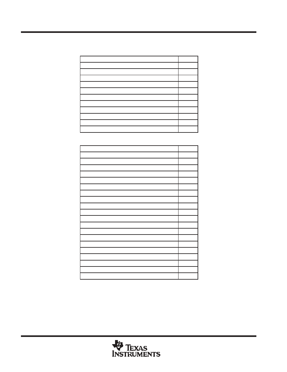
Figure 1
0.3
0.2
0.1
0
-50
-25
0
25
50
75
100
Shutdown Threshold V
o
ltage - V
0.4
0.5
SHUTDOWN THRESHOLD VOLTAGE
vs
FREE-AIR TEMPERATURE
0.6
TA - Free-Air Temperature -
∞
C
V(FB/SD)
Figure 2
2
1
0
0
5
10
15
- Supply Current - mA
3
4
SUPPLY CURRENT
vs
INPUT VOLTAGE
5
CC
I
IO = 0
VCC - Input Voltage - V
25
15
-50
-25
0
25
50
75
Oscillator Frequency - kHz
OSCILLATOR FREQUENCY
vs
FREE-AIR TEMPERATURE
35
100
21
VCC = 15 V
VCC = 3.5 V
TA - Free-Air Temperature -
∞
C
19
17
23
27
29
31
33
Figure 3
Figure 4
60
40
20
0
0
5
Supply Current in Shutdown -
80
100
SUPPLY CURRENT IN SHUTDOWN
vs
INPUT VOLTAGE
120
10
15
µ
A
VCC - Input Voltage - V
V(FB/SD) = 0
Data at high and low temperatures are applicable only within the recommended operating free-air temperature range.