 | –≠–ª–µ–∫—Ç—Ä–æ–Ω–Ω—ã–π –∫–æ–º–ø–æ–Ω–µ–Ω—Ç: MAX222CDW | –°–∫–∞—á–∞—Ç—å:  PDF PDF  ZIP ZIP |
MAX222
5 V DUAL RS 232 LINE DRIVER/RECEIVER
WITH ±15 kV ESD PROTECTION
SLLS590 - SEPTEMBER 2003
1
POST OFFICE BOX 655303
∑
DALLAS, TEXAS 75265
D
ESD Protection for RS-232 Bus Pins
-
±
15-kV Human-Body Model
D
Meets or Exceeds the Requirements of
TIA/EIA-232-F and ITU v.28 Standards
D
Operates at 5-V V
CC
Supply
D
Operates Up To 200 kbit/s
D
Low Supply Current in Shutdown
Mode . . . 2
µ
A Typical
D
External Capacitors . . . 4
◊
0.1
µ
F
D
Designed to Be Interchangeable With
Maxim MAX222
D
Latch-Up Performance Exceeds 100 mA Per
JESD 78, Class II
D
Applications
- Battery-Powered Systems, PDAs,
Notebooks, Laptops, Palmtop PCs, and
Hand-Held Equipment
description/ordering information
The MAX222 consists of two line drivers, two line receivers, and a dual charge-pump circuit with
±
15-kV ESD
protection pin to pin (serial-port connection pins, including GND). This device meets the requirements of
TIA/EIA-232-F and provides the electrical interface between an asynchronous communication controller and
the serial-port connector. The charge pump and four small external capacitors allow operation from a single 5-V
supply. This device operates at data signaling rates up to 200 kbit/s and a maximum of 30-V/
µ
s driver output
slew rate. By using SHDN, all receivers can be disabled.
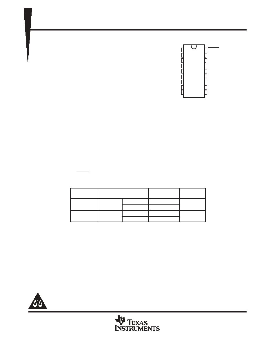
ORDERING INFORMATION
TA
PACKAGE
ORDERABLE
PART NUMBER
TOP-SIDE
MARKING
0
∞
C to 70
∞
C
SOIC (DW)
Tube of 20
MAX222CDW
MAX222C
0
∞
C to 70
∞
C
SOIC (DW)
Reel of 1000
MAX222CDWR
MAX222C
- 40
∞
C to 85
∞
C
SOIC (DW)
Tube of 20
MAX222IDW
MAX222I
- 40
∞
C to 85
∞
C
SOIC (DW)
Reel of 1000
MAX222IDWR
MAX222I
Package drawings, standard packing quantities, thermal data, symbolization, and PCB
design guidelines are available at www.ti.com/sc/package.
Copyright
2003, Texas Instruments Incorporated
Please be aware that an important notice concerning availability, standard warranty, and use in critical applications of
Texas Instruments semiconductor products and disclaimers thereto appears at the end of this data sheet.
DW PACKAGE
(TOP VIEW)
1
2
3
4
5
6
7
8
9
18
17
16
15
14
13
12
11
10
NC
C1+
V+
C1-
C2+
C2-
V-
DOUT2
RIN2
SHDN
V
CC
GND
DOUT1
RIN1
ROUT1
DIN1
DIN2
ROUT2
PRODUCTION DATA information is current as of publication date.
Products conform to specifications per the terms of Texas Instruments
standard warranty. Production processing does not necessarily include
testing of all parameters.
MAX222
5 V DUAL RS 232 LINE DRIVER/RECEIVER
WITH ±15 kV ESD PROTECTION
SLLS590 - SEPTEMBER 2003
2
POST OFFICE BOX 655303
∑
DALLAS, TEXAS 75265
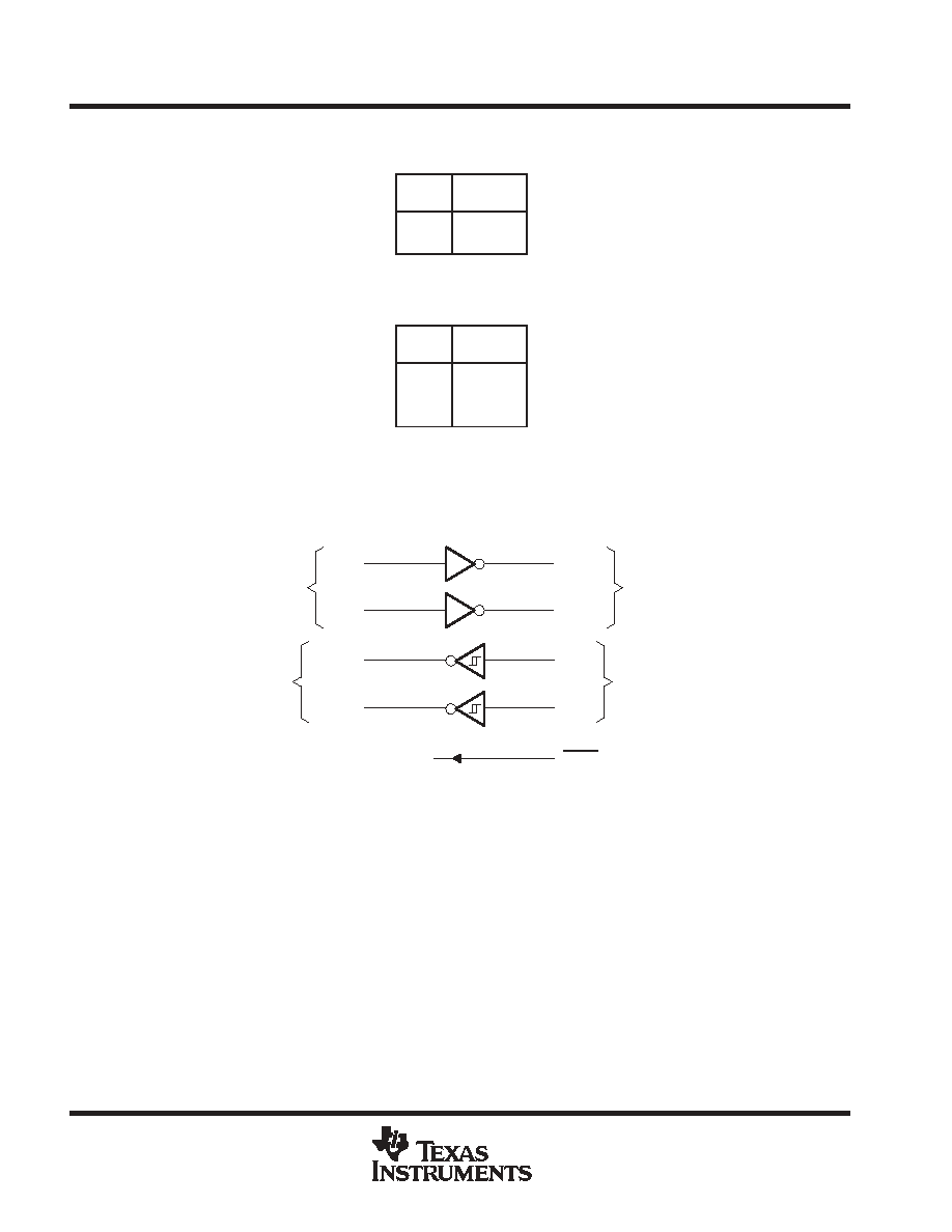
Function Tables
EACH DRIVER
INPUT
DIN
OUTPUT
DOUT
L
H
H
L
H = high level, L = low
level
EACH RECEIVER
INPUT
RIN
OUTPUT
ROUT
L
H
H
L
Open
H
H = high level, L = low
level, Open = input
disconnected or
connected driver off
logic diagram (positive logic)
DIN1
DOUT1
RIN1
ROUT1
DIN2
DOUT2
RIN2
ROUT2
12
11
13
10
15
8
14
9
RS-232
Outputs
RS-232
Inputs
TTC/CMOS
Inputs
TTC/CMOS
Outputs
SHDN
18
MAX222
5 V DUAL RS 232 LINE DRIVER/RECEIVER
WITH ±15 kV ESD PROTECTION
SLLS590 - SEPTEMBER 2003
3
POST OFFICE BOX 655303
∑
DALLAS, TEXAS 75265
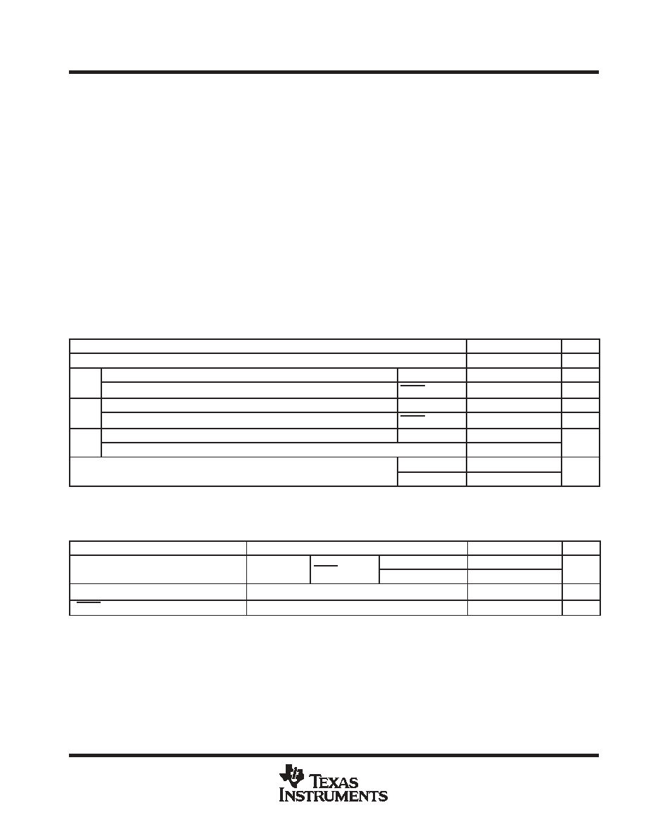
absolute maximum ratings over operating free-air temperature range (unless otherwise noted)
Supply voltage range, V
CC
(see Note 1)
-0.3 V to 6 V
. . . . . . . . . . . . . . . . . . . . . . . . . . . . . . . . . . . . . . . . . . . . . .
Input voltage range, V
I
: Drivers
-0.3 V to V
CC
-0.3 V
. . . . . . . . . . . . . . . . . . . . . . . . . . . . . . . . . . . . . . . . . . . . . . . .
Receivers
±
30 V
. . . . . . . . . . . . . . . . . . . . . . . . . . . . . . . . . . . . . . . . . . . . . . . . . . . . . . . . . .
Output voltage range, V
O
:Drivers
±
15 V
. . . . . . . . . . . . . . . . . . . . . . . . . . . . . . . . . . . . . . . . . . . . . . . . . . . . . . . . . .
Receivers
-0.3 V to V
CC
+ 0.3 V
. . . . . . . . . . . . . . . . . . . . . . . . . . . . . . . . . . . . . . . . . .
Short-circuit duration, D
OUT
Continuous
. . . . . . . . . . . . . . . . . . . . . . . . . . . . . . . . . . . . . . . . . . . . . . . . . . . . . . . . . . .
Package thermal impedance,
JA
(see Notes 2 and 3)
TBD
. . . . . . . . . . . . . . . . . . . . . . . . . . . . . . . . . . . . . . . . . .
Operating virtual junction temperature, T
J
150
∞
C
. . . . . . . . . . . . . . . . . . . . . . . . . . . . . . . . . . . . . . . . . . . . . . . . . . .
Lead temperature 1,6 mm (1/16 inch) from case for 10 seconds
260
∞
C
. . . . . . . . . . . . . . . . . . . . . . . . . . . . . . .
Storage temperature range, T
stg
-65
∞
C to 150
∞
C
. . . . . . . . . . . . . . . . . . . . . . . . . . . . . . . . . . . . . . . . . . . . . . . . . . .
Stresses beyond those listed under "absolute maximum ratings" may cause permanent damage to the device. These are stress ratings only, and
functional operation of the device at these or any other conditions beyond those indicated under "recommended operating conditions" is not
implied. Exposure to absolute-maximum-rated conditions for extended periods may affect device reliability.
NOTES:
1. All voltages are with respect to network GND.
2. Maximum power dissipation is a function of TJ(max),
JA, and TA. The maximum allowable power dissipation at any allowable
ambient temperature is PD = (TJ(max) - TA)/
JA. Operating at the absolute maximum TJ of 150
∞
C can affect reliability.
3. The package thermal impedance is calculated in accordance with JESD 51-7.
recommended operating conditions (see Note 4 and Figure 4)
MIN
NOM
MAX
UNIT
VCC
Supply voltage
4.5
5
5.5
V
VIH
Driver high-level input voltage
DIN
2
V
VIH
Shutdown high-level input voltage
SHDN
2
V
VIL
Driver low-level input voltage
DIN
0.8
V
VIL
Shutdown low-level input voltage
SHDN
0.8
V
VI
Driver input voltage
DIN
0
5.5
V
VI
Receiver input voltage
-30
30
V
TA
Operating free-air temperature
MAX222C
0
70
∞
C
TA
Operating free-air temperature
MAX222I
-40
85
∞
C
NOTE 4: Test conditions are C1-C4 = 0.1
µ
F at VCC = 5 V
±
0.5 V.
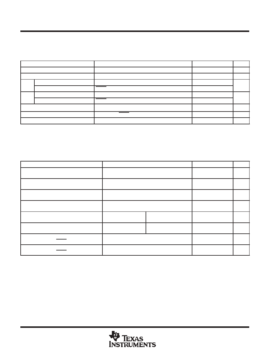
electrical characteristics over recommended ranges of supply voltage and operating free-air
temperature (unless otherwise noted) (see Note 4 and Figure 4)
PARAMETER
TEST CONDITIONS
MIN
TYP
MAX
UNIT
ICC
Supply current
VCC = 5 V
SHDN = VCC
No load
4
10
mA
ICC
Supply current
VCC = 5 V
SHDN = VCC
3 k
W
on both inputs
15
mA
Shutdown supply current
2
50
µ
A
SHDN
Shutdown input leakage current
±
1
µ
A
NOTE 4: Test conditions are C1-C4 = 0.1
µ
F at VCC = 5 V
±
0.5 V.
MAX222
5 V DUAL RS 232 LINE DRIVER/RECEIVER
WITH ±15 kV ESD PROTECTION
SLLS590 - SEPTEMBER 2003
4
POST OFFICE BOX 655303
∑
DALLAS, TEXAS 75265
DRIVER SECTION
electrical characteristics over recommended ranges of supply voltage and operating free-air
temperature (unless otherwise noted) (see Note 4 and Figure 4)
PARAMETER
TEST CONDITIONS
MIN
TYP
MAX
UNIT
VOH
High-level output voltage
DOUT at RL = 3 k
to GND,
DIN = GND
5
8
V
VOL
Low-level output voltage
DOUT at RL = 3 k
to GND,
DIN = VCC
-5
-8
V
IIH
Driver high-level input current
DIN = VCC
5
40
A
IIH
Control high-level input current
SHDN = VCC
0.01
1
µ
A
IIL
Driver low-level input current
DIN = 0 V
-5
-40
A
IIL
Control low-level input current
SHDN = 0 V
-0.01
-1
µ
A
IOS Short-circuit output current
VCC = 5.5 V,
VO = 0 V
±
7
±
22
mA
Output leakage current
VCC = 5.5 V, SHDN = GND,
VO =
±
15 V
±
0.01
±
10
µ
A
ro
Output resistance
VCC, V+, and V- = 0 V,
VO =
±
2 V
300
10 M
W
All typical values are at VCC = 5 V, and TA = 25
∞
C.
Short-circuit durations should be controlled to prevent exceeding the device absolute power dissipation ratings, and not more than one output
should be shorted at a time.
NOTE 4: Test conditions are C1-C4 = 0.1
µ
F at VCC = 5 V
±
0.5 V.
switching characteristics over recommended ranges of supply voltage and operating free-air
temperature (unless otherwise noted) (see Note 4 and Figure 4)
PARAMETER
TEST CONDITIONS
MIN
TYP
MAX
UNIT
Data rate
CL = 1000 pF,
One DOUT switching,
RL = 3 k
,
See Figure 1
200
kbit/s
tPLH (D)
Propagation delay time,
low- to high-level output
See Figure 1
1.5
3.5
µ
s
tPHL (D)
Propagation delay time,
high- to low-level output
See Figure 1
1.3
3.5
µ
s
tPHL (D) -
tPLH (D)
Driver (+ to -) propagation delay
difference
300
ns
tsk(p)
Pulse skewß
CL = 150 pF to 2500 pF
RL = 3 k
to 7 k
,
See Figure 2
300
ns
SR(tr)
Slew rate, transition region
(see Figure 1)
RL = 3 k
to 7 k
,
VCC = 5 V
CL = 50 pF to 2500 pF
6
12
30
V/
µ
s
tET
Driver output enable time
(after SHDN goes high)
250
µ
s
tDT
Driver output disable time
(after SHDN goes low)
300
ns
All typical values are at VCC = 5 V and TA = 25
∞
C.
ß Pulse skew is defined as |tPLH - tPHL| of each channel of the same device.
NOTE 4: Test conditions are C1-C4 = 0.1
µ
F at VCC = 5 V
±
0.5 V.
MAX222
5 V DUAL RS 232 LINE DRIVER/RECEIVER
WITH ±15 kV ESD PROTECTION
SLLS590 - SEPTEMBER 2003
5
POST OFFICE BOX 655303
∑
DALLAS, TEXAS 75265
RECEIVER SECTION
electrical characteristics over recommended ranges of supply voltage and operating free-air
temperature (unless otherwise noted) (see Note 4 and Figure 4)
PARAMETER
TEST CONDITIONS
MIN
TYP
MAX
UNIT
VOH
High-level output voltage
IOH = -1 mA
3.5
VCC-0.2 V
V
VOL
Low-level output voltage
IOL = 3.2 mA
0.4
V
VIT+
Positive-going input threshold voltage
VCC = 5 V
1.7
2.4
V
VIT-
Negative-going input threshold voltage
VCC = 5 V
0.8
1.3
V
Vhys
Input hysteresis (VIT+ - VIT-)
0.2
0.5
1
V
ri
Input resistance
VI =
±
3 V to
±
25 V
3
5
7
k
W
All typical values are at VCC = 5 V, and TA = 25
∞
C.
NOTE 4: Test conditions are C1-C4 = 0.1
µ
F at VCC = 5 V
±
0.5 V.
switching characteristics over recommended ranges of supply voltage and operating free-air
temperature (unless otherwise noted) (see Note 4 and Figure 3)
PARAMETER
TEST
CONDITIONS
MIN
TYP
MAX
UNIT
tPLH (R)
Propagation delay time, low- to high-level output
CL= 150 pF
0.6
1
µ
s
tPHL (R)
Propagation delay time, high- to low-level output
CL= 150 pF
0.5
1
µ
s
tPHL (R) -
tPLH (R)
Receiver (+ to -) propagation delay difference
100
ns
tsk(p)
Pulse skew
100
ns
All typical values are at VCC = 5 V and TA = 25
∞
C.
Pulse skew is defined as |tPLH - tPHL| of each channel of the same device.
NOTE 4: Test conditions are C1-C4 = 0.1
µ
F, at VCC = 5 V
±
0.5 V.
ESD protection
PIN
TEST CONDITIONS
TYP
UNIT
DOUT, RIN
Human-Body Model
±
15
kV