 | –≠–ª–µ–∫—Ç—Ä–æ–Ω–Ω—ã–π –∫–æ–º–ø–æ–Ω–µ–Ω—Ç: MAX4596 | –°–∫–∞—á–∞—Ç—å:  PDF PDF  ZIP ZIP |
MAX4596
SINGLE CHANNEL 10 W SPST ANALOG SWITCH
SLLS641 ≠ JANUARY 2005
Description
The MAX4596 is a single-pole single-throw (SPST)
analog switch that is designed to operate from 2 V to
5 V. This device can handle both digital and analog
signals, and signals up to V
+
(peak) can be transmitted
in either direction.
Applications
D
Sample-and-Hold Circuits
D
Battery-Powered Equipment
D
Audio and Video Signal Routing
D
Communication Circuits
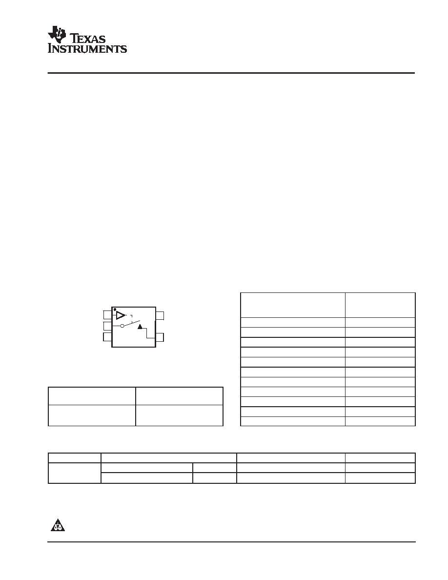
SOT-23 OR SC-70 PACKAGE
(TOP VIEW)
1
2
3
5
4
IN
COM
GND
NO
V+
FUNCTION TABLE
IN
NO TO COM,
COM TO NO
L
OFF
H
ON
Features
D
Low ON-State Resistance (10
W
)
D
ON-State Resistance Flatness (1.5
W
)
D
Control Inputs Are 5.5-V Tolerant
D
Low Charge Injection (5 pC Max)
D
300-MHz -3-dB Bandwidth at 25
5
C
D
Low Total Harmonic Distortion (THD) (0.05%)
D
2-V to 5.5-V Single-Supply Operation
D
Specified at 5-V and 3.3-V Nodes
D
-83-dB OFF Isolation at 1 MHz
D
Latch-Up Performance Exceeds 100 mA Per
JESD 78, Class II
D
0.5-nA Max OFF Leakage
D
ESD Performance Tested Per JESD 22
- 2000-V Human-Body Model
(A114-B, Class II)
- 1000-V Charged-Device Model (C101)
D
TTL/CMOS-Logic Compatible
Summary of Characteristics
V
+
= 5 V, T
A
= 25
∞
C
Configuration
Single Pole
Single Throw
(SPST)
Number of channels
1
ON-state resistance (ron)
10
ON-state resistance flatness (ron(flat))
1.5
Turn-on/turn-off time (tON/tOFF)
35 ns/40 ns
Charge injection (QC)
5 pC
Bandwidth (BW)
300 MHz
OFF isolation (OISO)
-83 dB at 1 MHz
Total harmonic distortion (THD)
0.05%
Leakage current (ICOM(OFF)/INO(OFF))
±
0.05 nA
Power-supply current (I+)
1
µ
A
Package option
5-pin SOT-23 or SC-70
ORDERING INFORMATION
TA
PACKAGE(1)
ORDERABLE PART NUMBER
TOP-SIDE MARKING(2)
-40
∞
C to 85
∞
C
SOT (SOT-23) - DBV
Tape and reel
MAX4596DBVR
6SB_
-40
∞
C to 85
∞
C
SOT (SC-70) - DCK
Tape and reel
MAX4596DCKR
SB_
(1) Package drawings, standard packing quantities, thermal data, symbolization, and PCB design guidelines are available at www.ti.com/sc/package.
(2) DBV/DCK: The actual top-side marking has one additional character that designates the assembly/test site.
Please be aware that an important notice concerning availability, standard warranty, and use in critical applications of Texas Instruments
semiconductor products and disclaimers thereto appears at the end of this data sheet.
www.ti.com
Copyright
2005, Texas Instruments Incorporated
PRODUCTION DATA information is current as of publication date.
Products conform to specifications per the terms of Texas Instruments
standard warranty. Production processing does not necessarily include
testing of all parameters.
MAX4596
SINGLE CHANNEL 10 W SPST ANALOG SWITCH
SLLS641 ≠ JANUARY 2005
www.ti.com
2
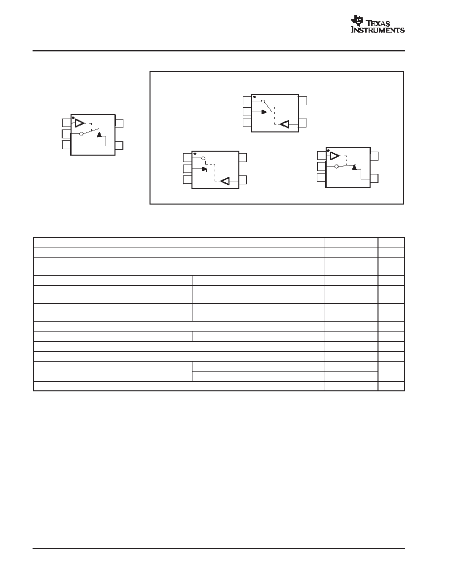
Pin Configurations
1
2
3
4
5
COM
NC
GND
IN
V+
1
2
3
4
5
COM
NO
GND
IN
V+
1
2
3
5
4
IN
COM
GND
NO
V+
1
2
3
5
4
IN
COM
GND
NC
V+
MAX4594
MAX4595
MAX4596
MAX4597
Available in Other Pin Configurations
Absolute Minimum and Maximum Ratings(1)(2)
over operating free-air temperature range (unless otherwise noted)
MIN
MAX
UNIT
V+
Supply voltage range(3)
-0.3
6
V
VNO
VCOM
Analog voltage range(3)(4)
-0.3
V+ + 0.3
V
IK
Analog port diode current
VNO, VCOM < 0
-50
mA
INO
ICOM
On-state switch current
VNO, VCOM = 0 to V+
-20
20
mA
INO
ICOM
On-state switch current
(pulsed at 1 ms, 10% duty cycle)
VNO, VCOM = 0 to V+
-40
40
mA
VI
Digital input voltage range(3)(4)
-0.3
6
V
IIK
Digital input clamp current
VI < 0
-50
mA
I+
Continuous current through V+
100
mA
IGND
Continuous current through GND
-100
mA
JA
Package thermal impedance(5)
DBV package
206
∞
C/W
JA
Package thermal impedance(5)
DCK package
252
∞
C/W
Tstg
Storage temperature range
-65
150
∞
C
(1) Stresses above these ratings may cause permanent damage. Exposure to absolute maximum conditions for extended periods may degrade
device reliability. These are stress ratings only, and functional operation of the device at these or any other conditions beyond those specified
is not implied.
(2) The algebraic convention, whereby the most negative value is a minimum and the most positive value is a maximum
(3) All voltages are with respect to ground, unless otherwise specified.
(4) The input and output voltage ratings may be exceeded if the input and output clamp-current ratings are observed.
(5) The package thermal impedance is calculated in accordance with JESD 51-7.
MAX4596
SINGLE CHANNEL 10 W SPST ANALOG SWITCH
SLLS641 ≠ JANUARY 2005
www.ti.com
3
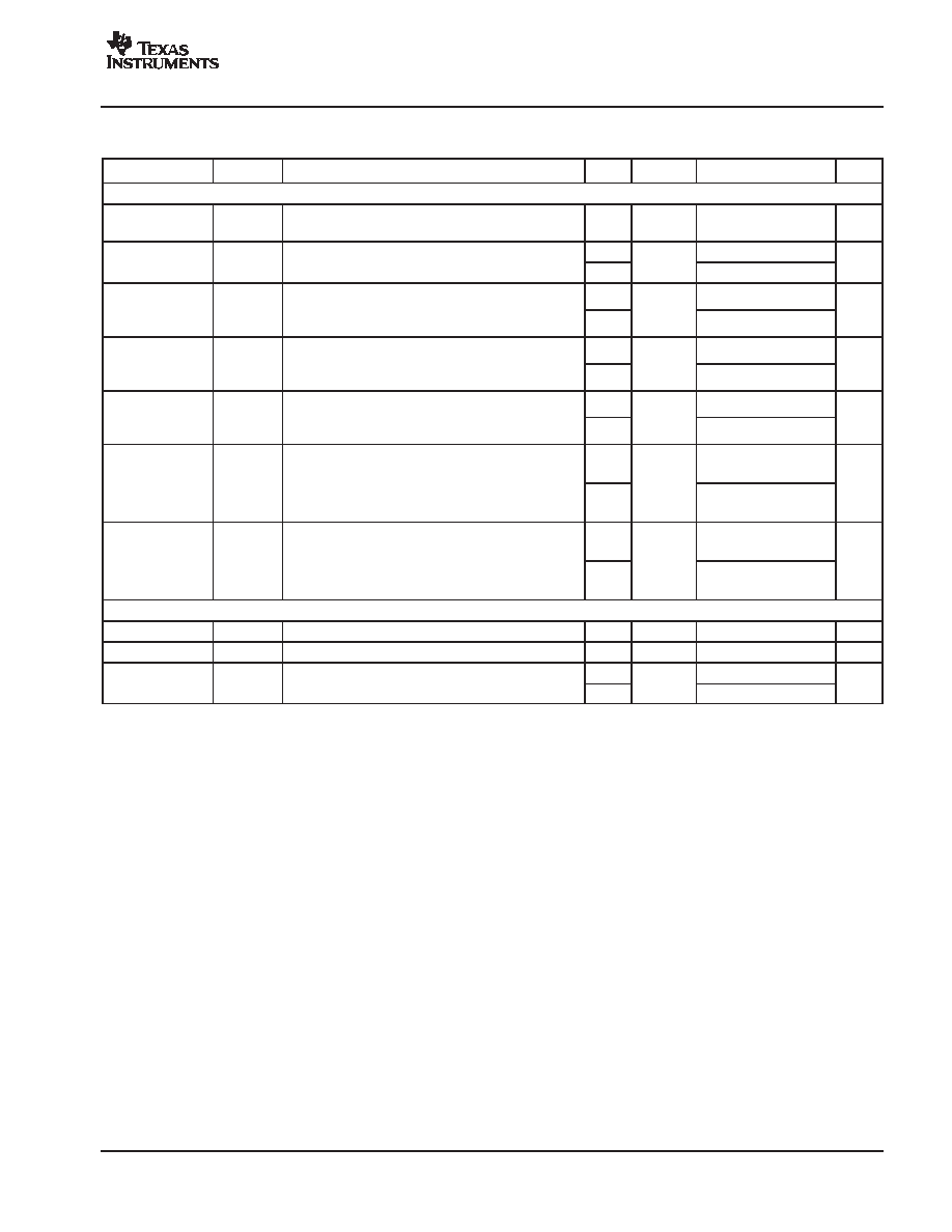
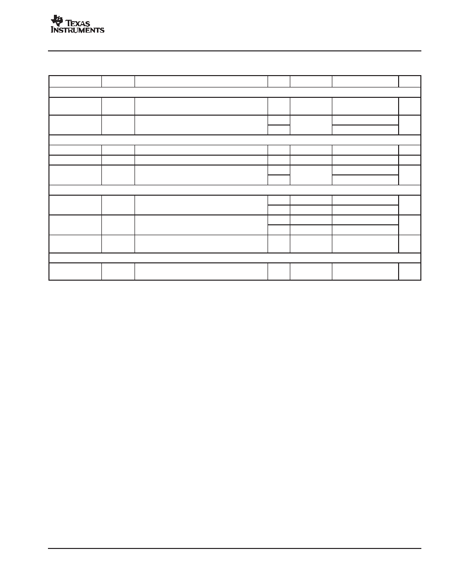
Electrical Characteristics for 5-V Supply
(1)
V+ = 4.5 V to 5.5 V, TA = -40
∞
C to 85
∞
C (unless otherwise noted)
PARAMETER
SYMBOL
TEST CONDITIONS
TA
V+
MIN
TYP
MAX
UNIT
Analog Switch
Analog signal
range
VCOM,
VNO
0
V+
V
ON-state
ron
VNO = 3.5 V
Switch ON,
25
∞
C
4.5 V
6.5
10
ON-state
resistance
ron
VNO = 3.5 V
ICOM = 10 mA,
Switch ON,
See Figure 13
Full
4.5 V
12
ON-state
resistance
ron(flat)
VNO = 1.5 V, 2.5 V, 3.5 V
Switch ON,
25
∞
C
4.5 V
0.5
1.5
resistance
flatness
ron(flat)
VNO = 1.5 V, 2.5 V, 3.5 V
ICOM = 10 mA,
Switch ON,
See Figure 13
Full
4.5 V
2
NO
OFF leakage
INO(OFF)
VNO = 1 V, VCOM = 4.5 V,
or
Switch OFF,
25
∞
C
5.5 V
-0.5
0.01
0.5
nA
OFF leakage
current
INO(OFF)
NO
COM
or
VNO = 4.5 V, VCOM = 1 V,
Switch OFF,
See Figure 14
Full
5.5 V
-5
5
nA
COM
OFF leakage
ICOM(OFF)
VCOM = 1 V, VNO = 4.5 V,
or
Switch OFF,
25
∞
C
5.5 V
-0.5
0.01
0.5
nA
OFF leakage
current
ICOM(OFF)
COM
NO
or
VCOM = 4.5 V, VNO = 1 V,
Switch OFF,
See Figure 14
Full
5.5 V
-5
5
nA
NO
ON leakage
INO(ON)
VNO = 1 V, VCOM = 1 V,
or
VNO = 4.5 V, VCOM = 4.5 V,
Switch ON,
25
∞
C
5.5 V
-1
0.01
1
nA
ON leakage
current
INO(ON)
or
VNO = 4.5 V, VCOM = 4.5 V,
or
VNO = 1 V, 4.5 V, VCOM = Open,
Switch ON,
See Figure 15
Full
5.5 V
-10
10
nA
COM
ON leakage
ICOM(ON)
VCOM = 1 V, VNO = 1 V,
or
VCOM = 4.5 V, VNO = 4.5 V,
Switch ON,
25
∞
C
5.5 V
-1
0.01
1
nA
ON leakage
current
ICOM(ON)
or
VCOM = 4.5 V, VNO = 4.5 V,
or
VCOM = 1 V, 4.5 V, VNO = Open,
Switch ON,
See Figure 15
Full
5.5 V
-10
10
nA
Digital Control Input (IN)
Input logic high
VIH
Full
2.4
5.5
V
Input logic low
VIL
Full
0
0.8
V
Input leakage
IIH, IIL
VI = V+ or 0
25
∞
C
5.5 V
-1
0.03
1
A
Input leakage
current
IIH, IIL
VI = V+ or 0
Full
5.5 V
-1
1
µ
A
(1) The algebraic convention, whereby the most negative value is a minimum and the most positive value is a maximum
MAX4596
SINGLE CHANNEL 10 W SPST ANALOG SWITCH
SLLS641 ≠ JANUARY 2005
www.ti.com
4
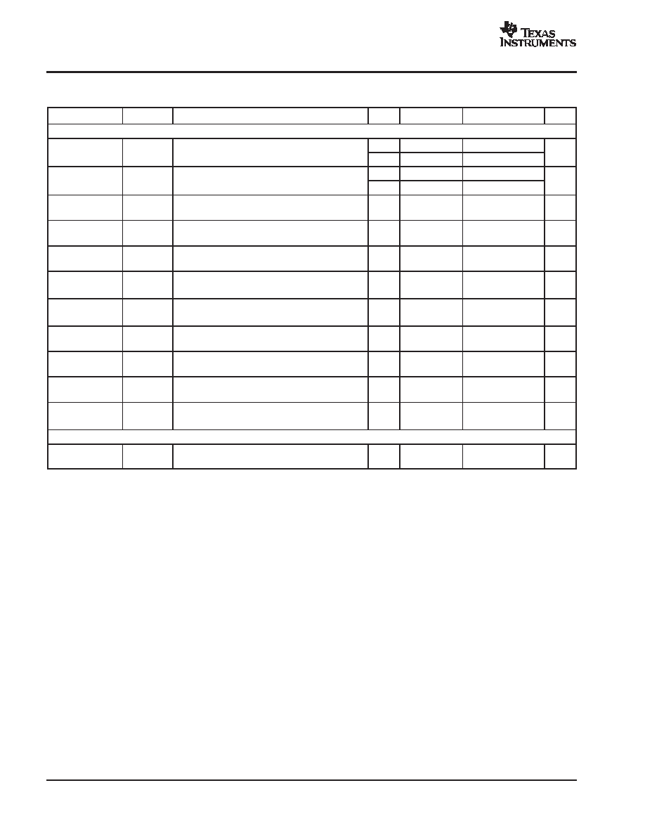
Electrical Characteristics for 5-V Supply
(1)
(continued)
V+ = 4.5 V to 5.5 V, TA = -40
∞
C to 85
∞
C (unless otherwise noted)
PARAMETER
SYMBOL
TEST CONDITIONS
TA
V+
MIN
TYP
MAX
UNIT
Dynamic
Turn-on time
tON
VNO = 3 V,
CL = 35 pF,
25
∞
C
5 V
20
35
ns
Turn-on time
tON
VNO = 3 V,
RL = 300
,
CL = 35 pF,
See Figure 17
Full
4.5 V to 5.5 V
45
ns
Turn-off time
tOFF
VCOM = 3 V,
CL = 35 pF,
25
∞
C
5 V
25
40
ns
Turn-off time
tOFF
VCOM = 3 V,
RL = 300
,
CL = 35 pF,
See Figure 17
Full
4.5 V to 5.5 V
50
ns
Charge injection
QC
VGEN = 0, RGEN = 0,
CL = 1 nF,
See Figure 20
25
∞
C
5 V
2
5
pC
NO
OFF capacitance
CNO(OFF)
VNO = V+ or GND,
f = 1 MHz,
Switch OFF,
See Figure 16
25
∞
C
5 V
8
pF
COM
OFF capacitance
CCOM(OFF)
VCOM = V+ or GND,
f = 1 MHz,
Switch OFF,
See Figure 16
25
∞
C
5 V
8
pF
NO
ON capacitance
CNO(ON))
VNO = V+ or GND,
f = 1 MHz,
Switch ON,
See Figure 16
25
∞
C
5 V
20
pF
COM
ON capacitance
CCOM(ON)
VCOM = V+ or GND,
f = 1 MHz,
Switch ON,
See Figure 16
25
∞
C
5 V
20
pF
Digital input
capacitance
CI
VI = V+ or GND,
See Figure 16
25
∞
C
5 V
3
pF
Bandwidth
BW
RL = 50
,
Signal = 0 dBm,
Switch ON,
See Figure 18
25
∞
C
5 V
300
MHz
OFF isolation
OISO
RL = 50
, CL = 5 pF,
VNO = 1 VRMS, f = 1 MHz,
Switch OFF,
See Figure 19
25
∞
C
5 V
-83
dB
Total harmonic
distortion
THD
RL = 600
, CL = 50 pF,
VSOURCE = 5 Vp-p,
f = 20 Hz to 20 kHz,
See Figure 21
25
∞
C
5 V
0.05
%
Supply
Positive supply
current
I+
VI = V+ or GND,
Switch ON or OFF
Full
5.5 V
1
µ
A
(1) The algebraic convention, whereby the most negative value is a minimum and the most positive value is a maximum
MAX4596
SINGLE CHANNEL 10 W SPST ANALOG SWITCH
SLLS641 ≠ JANUARY 2005
www.ti.com
5
Electrical Characteristics for 3-V Supply
(1)
V+ = 2.7 V to 3.6 V, TA = -40
∞
C to 85
∞
C (unless otherwise noted)
PARAMETER
SYMBOL
TEST CONDITIONS
TA
V+
MIN
TYP
MAX
UNIT
Analog Switch
Analog signal
range
VCOM,
VNO
0
V+
V
ON-state
ron
VNO = 1.5 V,
Switch ON,
25
∞
C
2.7 V
10
20
ON-state
resistance
ron
VNO = 1.5 V,
ICOM = 10 mA,
Switch ON,
See Figure 13
Full
2.7 V
25
Digital Control Input (IN)
Input logic high
VIH
Full
2
5.5
V
Input logic low
VIL
Full
0
0.8
V
Input leakage
IIH, IIL
VI = V+ or 0
25
∞
C
3.6 V
-1
0.03
1
A
Input leakage
current
IIH, IIL
VI = V+ or 0
Full
3.6 V
-1
1
µ
A
Dynamic
Turn-on time
tON
VNO = 2 V,
CL = 35 pF,
25
∞
C
3 V
25
45
ns
Turn-on time
tON
VNO = 2 V,
RL = 300
,
CL = 35 pF,
See Figure 17
Full
2.7 V to 3.6 V
55
ns
Turn-off time
tOFF
VNO = 2 V,
CL = 35 pF,
25
∞
C
3 V
30
50
ns
Turn-off time
tOFF
VNO = 2 V,
RL = 300
,
CL = 35 pF,
See Figure 17
Full
2.7 V to 3.6 V
60
ns
Charge injection
QC
VGEN = 0, RGEN = 0,
CL = 1 nF,
See Figure 20
25
∞
C
3 V
2
4
pC
Supply
Positive supply
current
I+
VI = V+ or GND,
Switch ON or OFF
Full
3.6 V
1
µ
A
(1) The algebraic convention, whereby the most negative value is a minimum and the most positive value is a maximum