1
2
3
6
5
4
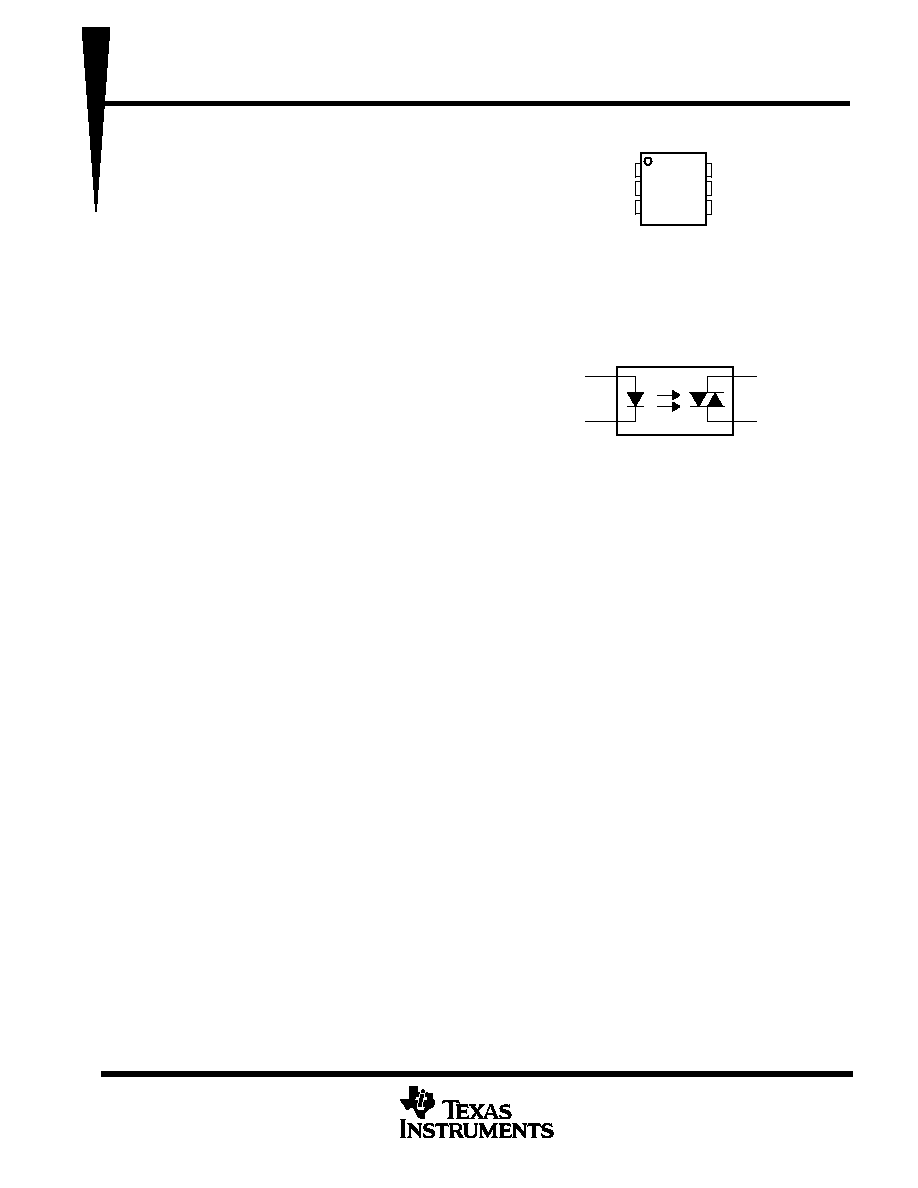
ANODE
CATHODE
NC
MAIN TERM
TRIAC SUB
MAIN TERM
MOC3020 ≠ MOC3023 . . . PACKAGE
(TOP VIEW)
NC ≠ No internal connection
Do not connect this terminal
logic diagram
6
4
1
2
MOC3020 THRU MOC3023
OPTOCOUPLERS/OPTOISOLATORS
SOES025 ≠ OCTOBER 1986 ≠ REVISED OCTOBER 1995
Copyright
©
1995, Texas Instruments Incorporated
7≠1
POST OFFICE BOX 655303
∑
DALLAS, TEXAS 75265
∑
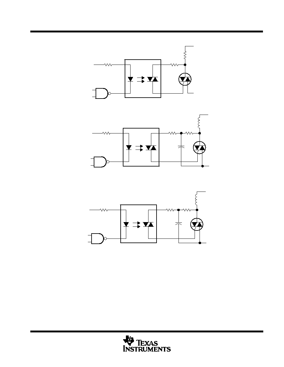
250 V Phototriac Driver Output
∑
Gallium-Arsenide-Diode Infrared Source and
Optically-Coupled Silicon Traic Driver
(Bilateral Switch)
∑
UL Recognized
File Number E65085
. . .
∑
High Isolation
7500 V Peak
. . .
∑
Output Driver Designed for 220 V ac
∑
Standard 6-Terminal Plastic DIP
∑
Directly Interchangeable with
Motorola MOC3020, MOC3021, MOC3022,
and MOC3023
∑
Direct Replacements for:
≠ TRW Optron OPI3020, OPI3021,
OPI3022, and OPI3023;
≠ General Instrument MCP3020,
MCP3021, and MCP3022;
≠ General Electric GE3020,
GE3021, GE3022, and GE3023
absolute maximum ratings at 25
∞
C free-air temperature (unless otherwise noted)
Input-to-output peak voltage, 5 s maximum duration, 60 Hz (see Note 1)
7.5 kV
. . . . . . . . . . . . . . . . . . . . . . . .
Input diode reverse voltage
3 V
. . . . . . . . . . . . . . . . . . . . . . . . . . . . . . . . . . . . . . . . . . . . . . . . . . . . . . . . . . . . . . . . . .
Input diode forward current, continuous
50 mA
. . . . . . . . . . . . . . . . . . . . . . . . . . . . . . . . . . . . . . . . . . . . . . . . . . . . .
Output repetitive peak off-state voltage
400 V
. . . . . . . . . . . . . . . . . . . . . . . . . . . . . . . . . . . . . . . . . . . . . . . . . . . . .
Output on-state current, total rms value (50-60 Hz, full sine wave): T
A
= 25
∞
C
100 mA
. . . . . . . . . . . . . . . . . . .
T
A
= 70
∞
C
50 mA
. . . . . . . . . . . . . . . . . . . .
Output driver nonrepetitive peak on-state current (t
w
= 10 ms, duty cycle = 10%, see Figure 7)
1.2 A
. . . . . .
Continuous power dissipation at (or below) 25
∞
C free-air temperature:
Infrared-emitting diode (see Note 2)
100 mW
. . . . . . . . . . . . . . . . . . . . . . . . . . . . . . . . . . . . . . . . . . . . . . . . .
Phototriac (see Note 3)
300 mW
. . . . . . . . . . . . . . . . . . . . . . . . . . . . . . . . . . . . . . . . . . . . . . . . . . . . . . . . . . . .
Total device (see Note 4)
330 mW
. . . . . . . . . . . . . . . . . . . . . . . . . . . . . . . . . . . . . . . . . . . . . . . . . . . . . . . . . . .
Operating junction temperature range, T
J
≠ 40
∞
C to 100
∞
C
. . . . . . . . . . . . . . . . . . . . . . . . . . . . . . . . . . . . . . . . . .
Storage temperature range, T
stg
≠ 40
∞
C to 150
∞
C
. . . . . . . . . . . . . . . . . . . . . . . . . . . . . . . . . . . . . . . . . . . . . . . . . .
Lead temperature 1,6 (1/16 inch) from case for 10 seconds
260
∞
C
. . . . . . . . . . . . . . . . . . . . . . . . . . . . . . . . . . .
Stresses beyond those listed under "absolute maximum ratings" may cause permanent damage to the device. These are stress ratings only, and
functional operation of the device at these or any other conditions beyond those indicated under "recommended operating conditions" is not
implied. Exposure to absolute-maximum-rated conditions for extended periods may affect device reliability.
NOTES:
1. Input-to-output peak voltage is the internal device dielectric breakdown rating.
2. Derate linearly to 100
∞
C free-air temperature at the rate of 1.33 mW/
∞
C.
3. Derate linearly to 100
∞
C free-air temperature at the rate of 4 mW/
∞
C.
4. Derate linearly to 100
∞
C free-air temperature at the rate of 4.4 mW/
∞
C.
PRODUCTION DATA information is current as of publication date.
Products conform to specifications per the terms of Texas Instruments
standard warranty. Production processing does not necessarily include
testing of all parameters.
MOC3020 THRU MOC3023
OPTOCOUPLERS/OPTOISOLATORS
SOES025 ≠ OCTOBER 1986 ≠ REVISED OCTOBER 1995
7≠2
POST OFFICE BOX 655303
∑
DALLAS, TEXAS 75265
electrical characteristics at 25
∞
C free-air temperature (unless otherwise noted)
PARAMETER
TEST CONDITIONS
MIN
TYP
MAX
UNIT
IR
Static reverse current
VR = 3 V
0.05
100
µ
A
VF
Static forward voltage
IF = 10 mA
1.2
1.5
V
I(DRM)
Repetitive off-state current, either direction
V(DRM) = 400 V,
See Note 5
10
100
nA
dv/dt
Critical rate of rise of off-state voltage
See Figure 1
100
V/
µ
s
dv/dt(c)
Critical rate of rise of commutating voltage
IO = 15 mA,
See Figure 1
0.15
V/
µ
s
I
I
i
MOC3020
O
l
l
3 V
15
30
A
IFT
Input trigger current,
MOC3021
Output supply voltage = 3 V
8
15
mA
IFT
Input trigger current,
either direction
MOC3022
Output supply voltage = 3 V
5
10
mA
MOC3023
3
5
VTM
Peak on-state voltage, either direction
ITM = 100 mA
1.4
3
V
IH
Holding current, either direction
100
µ
A
NOTE 5: Test voltage must be applied at a rate no higher than 12 V/
µ
s.
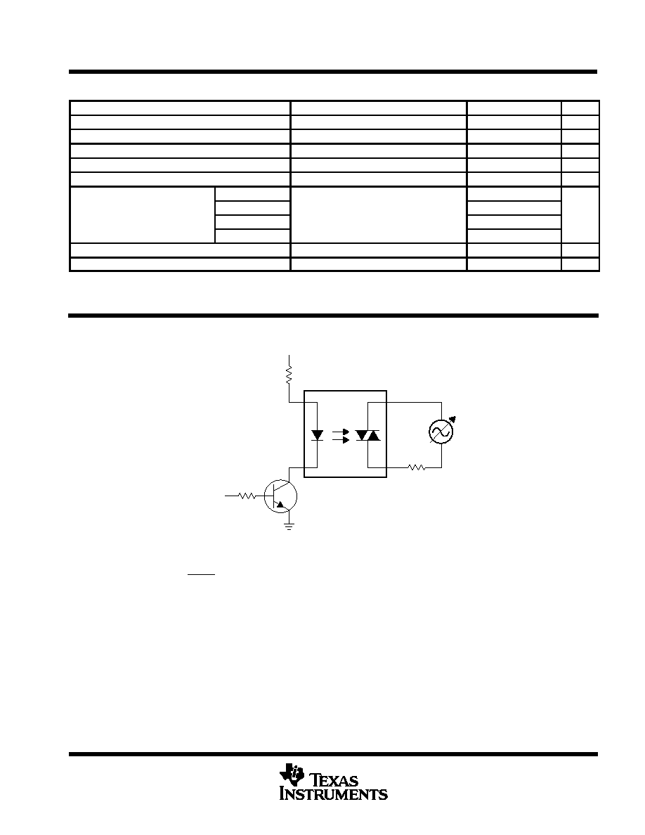
PARAMETER MEASUREMENT INFORMATION
NOTE A. The critical rate of rise of off-state voltage, dv/dt, is measured with the input at 0 V. The frequency of Vin is increased until the
phototriac turns on. This frequency is then used to calculate the dv/dt according to the formula:
The critical rate of rise of commutating voltage, dv/dt(c), is measured by applying occasional 5-V pulses to the input and increasing
the frequency of Vin until the phototriac stays on (latches) after the input pulse has ceased. With no further input pulses, the
frequency of Vin is then gradually decreased until the phototriac turns off. The frequency at which turn-off occurs may then be used
to calculate the dv/dt(c) according to the formula shown above.
dv dt
+
2
2
fV
in
6
4
RL
1
2
2N3904
10 k
VCC
VI = 30 V rms
Input
(see Note A)
Figure 1. Critical Rate of Rise Test Circuit
MOC3020 THRU MOC3023
OPTOCOUPLERS/OPTOISOLATORS
SOES025 ≠ OCTOBER 1986 ≠ REVISED OCTOBER 1995
7≠5
POST OFFICE BOX 655303
∑
DALLAS, TEXAS 75265
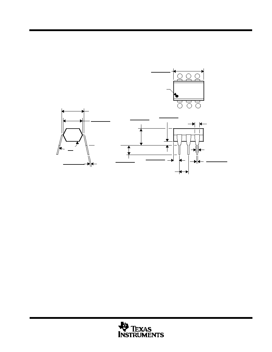
MECHANICAL INFORMATION
Each device consists of a gallium-arsenide infrared-emitting diode optically coupled to a silicon phototriac
mounted on a 6-terminal lead frame encapsulated within an electrically nonconductive plastic compound. The
case can withstand soldering temperature with no deformation and device performance characteristics remain
stable when operated in high-humidity conditions.
C
0,534 (0.021)
0,381 (0.015)
6 Places
Seating Plane
C
L
L
7,62 (0.300) T.P.
(see Note A)
6,61 (0.260)
6,09 (0.240)
0,305 (0.012)
0,203 (0.008)
3,81 (0.150)
3,17 (0.125)
5,46 (0.215)
2,95 (0.116)
1,78 (0.070)
0,51 (0.020)
2,03 (0.080)
1,52 (0.060)
4 Places
2,54 (0.100) T.P.
(see Note A)
1,01 (0.040) MIN
1,78 (0.070) MAX
6 Places
9,40 (0.370)
8,38 (0.330)
Index Dot
(see Note B)
105
∞
90
∞
1
2
3
6
5
4
(see Note C)
NOTES: A. Leads are within 0,13 (0.005) radius of true position (T.P.) with maximum material condition and unit installed.
B. Pin 1 identified by index dot.
C. Terminal connections:
1. Anode (part of the infrared-emitting diode)
2. Cathode (part of the infrared-emitting diode)
3. No internal connection
4. Main terminal (part of the phototransistor)
5. Triac Substrate (DO NOT connect) (part of the phototransistor)
6. Main terminal (part of the phototransistor)
D. The dimensions given fall within JEDEC MO-001 AM dimensions.
E. All linear dimensions are given in millimeters and parenthetically given in inches.
Figure 8. Mechanical Information