
FEATURES
ANALOG FEATURES
D
24 Bits No Missing Codes
D
22 Bits Effective Resolution at 10Hz
- Low Noise: 75nV
D
PGA From 1 to 128
D
Precision On-Chip Voltage Reference
- Accuracy: 0.2%
- Drift: 5ppm/
į
C
D
8 Differential/Single-Ended Channels
D
On-Chip Offset/Gain Calibration
D
Offset Drift: 0.02ppm/
į
C
D
Gain Drift: 0.5ppm/
į
C
D
On-Chip Temperature Sensor
D
Burnout Sensor Detection
D
Single-Cycle Conversion
D
Selectable Buffer Input
DIGITAL FEATURES
Microcontroller Core
D
8051-Compatible
D
High-Speed Core
- 4 Clocks per Instruction Cycle
D
DC to 33MHz
D
Single Instruction 121ns
D
Dual Data Pointer
Memory
D
Up To 32kB Flash Memory
D
Flash Memory Partitioning
D
Endurance 1M Erase/Write Cycles,
100 Year Data Retention
D
In-System Serially Programmable
D
External Program/Data Memory (64kB)
D
1,280 Bytes Data SRAM
D
Flash Memory Security
D
2kB Boot ROM
D
Programmable Wait State Control
Peripheral Features
D
34 I/O Pins
D
Additional 32-Bit Accumulator
D
Three 16-Bit Timer/Counters
D
System Timers
D
Programmable Watchdog Timer
D
Full-Duplex Dual USARTs
D
Master/Slave SPI
D
16-Bit PWM
D
Power Management Control
D
Idle Mode Current < 1mA
D
Stop Mode Current < 1
m
A
D
Programmable Brownout Reset
D
Programmable Low Voltage Detect
D
21 Interrupt Sources
D
Two Hardware Breakpoints
GENERAL FEATURES
D
Pin-Compatible with MSC1211/12/13/14
D
Package: TQFP-64
D
Low Power: 4mW
D
Industrial Temperature Range:
-40
į
C to +85
į
C
D
Power Supply: 2.7V to 5.25V
APPLICATIONS
D
Industrial Process Control
D
Instrumentation
D
Liquid/Gas Chromatography
D
Blood Analysis
D
Smart Transmitters
D
Portable Instruments
D
Weigh Scales
D
Pressure Transducers
D
Intelligent Sensors
D
Portable Applications
D
DAS Systems
MSC1210
SBAS203F - MARCH 2002 - REVISED NOVEMBER 2004
Precision Analog-to-Digital Converter (ADC)
with 8051 Microcontroller and Flash Memory
PRODUCTION DATA information is current as of publication date. Products
conform to specifications per the terms of Texas Instruments standard warranty.
Production processing does not necessarily include testing of all parameters.
www.ti.com
Copyright
2002-2004, Texas Instruments Incorporated
Please be aware that an important notice concerning availability, standard warranty, and use in critical applications of Texas Instruments
semiconductor products and disclaimers thereto appears at the end of this data sheet.
All trademarks are the property of their respective owners.
MSC1210
SBAS203F - MARCH 2002 - REVISED NOVEMBER 2004
www.ti.com
2
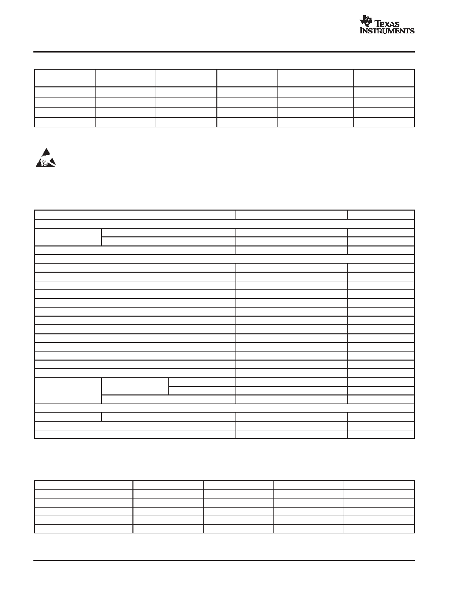
PACKAGE/ORDERING INFORMATION
(1)
PRODUCT
FLASH MEMORY
PACKAGE-LEAD
PACKAGE
DESIGNATOR
SPECIFIED
TEMPERATURE RANGE
PACKAGE
MARKING
MSC1210Y2
4k
TQFP-64
PAG
-40
į
C to +85
į
C
MSC1210Y2
MSC1210Y2
4k
TQFP-64
PAG
-40
į
C to +85
į
C
MSC1210Y2
MSC1210Y3
8k
TQFP-64
PAG
-40
į
C to +85
į
C
MSC1210Y3
MSC1210Y3
8k
TQFP-64
PAG
-40
į
C to +85
į
C
MSC1210Y3
MSC1210Y4
16k
TQFP-64
PAG
-40
į
C to +85
į
C
MSC1210Y4
MSC1210Y4
16k
TQFP-64
PAG
-40
į
C to +85
į
C
MSC1210Y4
MSC1210Y5
32k
TQFP-64
PAG
-40
į
C to +85
į
C
MSC1210Y5
MSC1210Y5
32k
TQFP-64
PAG
-40
į
C to +85
į
C
MSC1210Y5
(1) For the most current package and ordering information, see the Package Option Addendum at the end of this datasheet, or refer to our web site at www.ti.com.
This integrated circuit can be damaged by ESD. Texas Instruments recommends that all integrated circuits be handled
with appropriate precautions. Failure to observe proper handling and installation procedures can cause damage.
ESD damage can range from subtle performance degradation to complete device failure. Precision integrated circuits may be more
susceptible to damage because very small parametric changes could cause the device not to meet its published specifications.
ABSOLUTE MAXIMUM RATINGS
(1)
MSC1210Yx
UNITS
Analog Inputs
Input current
Momentary
100
mA
Input current
Continuous
10
mA
Input voltage
AGND - 0.3 to AVDD + 0.3
V
Power Supply
DVDD to DGND
-0.3 to +6
V
AVDD to AGND
-0.3 to +6
V
AGND to DGND
-0.3 to +0.3
V
VREF to AGND
-0.3 to AVDD + 0.3
V
Digital input voltage to DGND
-0.3 to DVDD + 0.3
V
Digital output voltage to DGND
-0.3 to DVDD + 0.3
V
Maximum junction temperature
150
į
C
Operating temperature range
-40 to +85
į
C
Storage temperature range
-65 to +150
į
C
Lead temperature (soldering, 10s)
+235
į
C
Package power dissipation
(TJ Max - TAMBIENT)/
q
JA
W
Output current, all pins
200
mA
Output pin short-circuit
10
s
Junction to ambient (
q
JA)
High K (2s 2p)
62.9
į
C/W
Thermal Resistance
Junction to ambient (
q
JA)
Low K (1s)
78.2
į
C/W
Thermal Resistance
Junction to case (
q
JC)
13.8
į
C/W
Digital Outputs
Output current
Continuous
100
mA
I/O source/sink current
100
mA
Power pin maximum
300
mA
(1) Stresses above those listed under Absolute Maximum Ratings may cause permanent damage to the device. Exposure to absolute maximum conditions for
extended periods may affect device reliability.
MSC1210YX FAMILY FEATURES
FEATURES(1)
MSC1210Y2(2)
MSC1210Y3(2)
MSC1210Y4(2)
MSC1210Y5(2)
Flash Program Memory (Bytes)
Up to 4k
Up to 8k
Up to 16k
Up to 32k
Flash Data Memory (Bytes)
Up to 4k
Up to 8k
Up to 16k
Up to 32k
Internal Scratchpad RAM (Bytes)
256
256
256
256
Internal MOVX RAM (Bytes)
1024
1024
1024
1024
Externally Accessible Memory (Bytes)
64k Program, 64k Data
64k Program, 64k Data
64k Program, 64k Data
64k Program, 64k Data
(1) All peripheral features are the same on all devices; the flash memory size is the only difference.
(2) The last digit of the part number (N) represents the onboard flash size = (2N)kBytes.
MSC1210
SBAS203F - MARCH 2002 - REVISED NOVEMBER 2004
www.ti.com
3
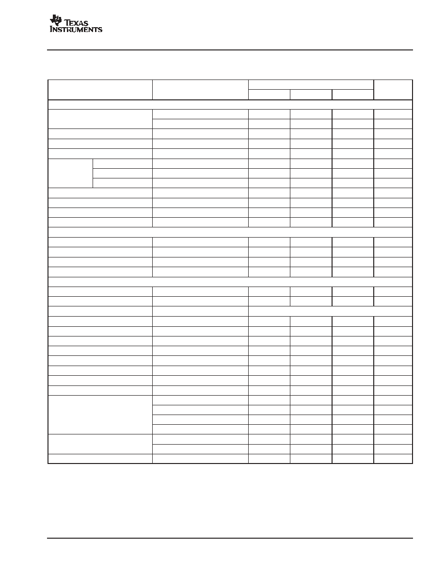
ELECTRICAL CHARACTERISTICS: AV
DD
= 5V
All specifications from TMIN to TMAX, DVDD = +2.7V to 5.25V, fMOD = 15.625kHz, PGA = 1, Buffer ON, fDATA = 10Hz, Bipolar, and VREF = (REF IN+) - (REF IN-) =
+2.5V, unless otherwise noted.
MSC1210Yx
PARAMETER
CONDITIONS
MIN
TYP
MAX
UNITS
Analog Input (AIN0-AIN7, AINCOM)
Analog Input Range
Buffer OFF
AGND - 0.1
AVDD + 0.1
V
Analog Input Range
Buffer ON
AGND + 50mV
AVDD - 1.5
V
Full-Scale Input Voltage Range
(In+) - (In-)
Ī
VREF/PGA
V
Differential Input Impedance
Buffer OFF
7/PGA
(5)
M
Input Current
Buffer ON
0.5
nA
Fast Settling Filter
-3dB
0.469
∑
fDATA
Bandwidth
Sinc2 Filter
-3dB
0.318
∑
fDATA
Bandwidth
Sinc3 Filter
-3dB
0.262
∑
fDATA
Programmable Gain Amplifier
User-Selectable Gain Range
1
128
Input Capacitance
Buffer On
9
pF
Input Leakage Current
Modulator OFF, T = +25
į
C
0.5
pA
Burnout Current Sources
Buffer On
Ī
2
Ķ
A
Offset DAC
Offset DAC Range
Ī
VREF/(2
∑
PGA)
V
Offset DAC Monotonicity
8
Bits
Offset DAC Gain Error
Ī
1.5
% of Range
Offset DAC Gain Error Drift
1
ppm/
į
C
System Performance
Resolution
24
Bits
ENOB
See Typical Characteristics
22
Bits
Output Noise
See Typical Characteristics
No Missing Codes
Sinc3 Filter, Decimation > 360
24
Bits
Integral Nonlinearity
End Point Fit, Differential Input
Ī
0.0015
% of FSR
Offset Error
After Calibration
7.5
ppm of FS
Offset Drift
(1)
Before Calibration
0.02
ppm of FS/
į
C
Gain Error
(2)
After Calibration
0.002
%
Gain Error Drift
(1)
Before Calibration
0.5
ppm/
į
C
System Gain Calibration Range
80
120
% of FS
System Offset Calibration Range
-50
50
% of FS
At DC
100
115
dB
ADC Common-Mode Rejection
fCM = 60Hz, fDATA = 10Hz
130
dB
ADC Common-Mode Rejection
fCM = 50Hz, fDATA = 50Hz
120
dB
fCM = 60Hz, fDATA = 60Hz
120
dB
Normal-Mode Rejection
fSIG = 50Hz, fDATA = 50Hz
100
dB
Normal-Mode Rejection
fSIG = 60Hz, fDATA = 60Hz
100
dB
Power-Supply Rejection
At DC, dB = -20log(
VOUT/
VDD)(3)
80
88
dB
(1)
Calibration can minimize these errors.
(2)
The gain calibration cannot have a REF IN+ of more than
AVDD -1.5V with Buffer ON. To calibrate gain, turn Buffer OFF.
(3)
VOUT is change in digital result.
(4)
9pF switched capacitor at
fSAMP clock frequency (see Figure 13).
(5)
The input impedance for PGA = 128 is the same as that for PGA = 64 (that is, 7M
/64).
MSC1210
SBAS203F - MARCH 2002 - REVISED NOVEMBER 2004
www.ti.com
4
ELECTRICAL CHARACTERISTICS: AV
DD
= 5V (continued)
All specifications from TMIN to TMAX, DVDD = +2.7V to 5.25V, fMOD = 15.625kHz, PGA = 1, Buffer ON, fDATA = 10Hz, Bipolar, and VREF = (REF IN+) - (REF IN-) =
+2.5V, unless otherwise noted.
MSC1210Yx
PARAMETER
UNITS
MAX
TYP
MIN
CONDITIONS
Voltage Reference Input
Reference Input Range
REF IN+, REF IN-
AGND
AVDD
(2)
V
VREF
VREF = (REF IN+) - (REF IN-)
0.1
2.5
AVDD
V
VREF Common-Mode Rejection
At DC
130
dB
VREF Common-Mode Rejection
fCM = 60Hz, fDATA = 60Hz
120
dB
Input Current
(4)
VREF = 2.5V
3
Ķ
A
On-Chip Voltage Reference
Output Voltage
VREFH = 1 at +25
į
C, ACLK = 1MHz
2.495
2.5
2.505
V
Output Voltage
VREFH = 0 at +25
į
C, ACLK = 1MHz
1.25
V
Power-Supply Rejection Ratio
65
dB
Short-Circuit Current Source
8
mA
Short-Circuit Current Sink
50
Ķ
A
Short-Circuit Duration
Sink or Source
Indefinite
Drift
5
ppm/
į
C
Output Impedance
Sourcing 100
Ķ
A
3
Startup Time from Power On
CREF = 0.1
Ķ
F
8
ms
Temperature Sensor Voltage
T = +25
į
C
115
mV
Temperature Sensor Coefficient
375
Ķ
V/
į
C
Analog Power-Supply Requirements
Analog Power-Supply Voltage
AVDD
4.75
5.0
5.25
V
Analog Current
(IADC + IVREF)
PDADC = 1, ALVDIS = 1, DAB = 1
< 1
nA
PGA = 1, Buffer OFF
200
Ķ
A
Analog
Power-Supply
ADC Current
PGA = 128, Buffer OFF
500
Ķ
A
Power-Supply
Current
ADC Current
(IADC)
PGA = 1, Buffer ON
240
Ķ
A
Current
ADC
PGA = 128, Buffer ON
850
Ķ
A
VREF Supply Current
(IVREF)
ADC ON, VDAC OFF
250
Ķ
A
(1)
Calibration can minimize these errors.
(2)
The gain calibration cannot have a REF IN+ of more than
AVDD -1.5V with Buffer ON. To calibrate gain, turn Buffer OFF.
(3)
VOUT is change in digital result.
(4)
9pF switched capacitor at
fSAMP clock frequency (see Figure 13).
(5)
The input impedance for PGA = 128 is the same as that for PGA = 64 (that is, 7M
/64).

MSC1210
SBAS203F - MARCH 2002 - REVISED NOVEMBER 2004
www.ti.com
5
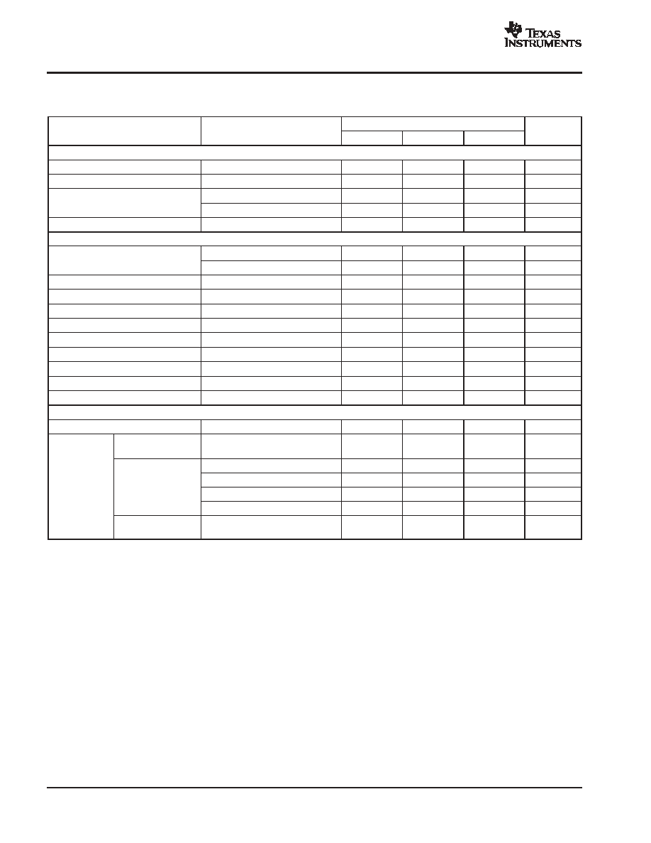
ELECTRICAL CHARACTERISTICS: AV
DD
= 3V
All specifications from TMIN to TMAX, DVDD = +2.7V to 5.25V, fMOD = 15.625kHz, PGA = 1, Buffer ON, fDATA = 10Hz, Bipolar, and VREF = (REF IN+) - (REF IN-) =
+1.25V, unless otherwise noted.
MSC1210Yx
PARAMETER
CONDITIONS
MIN
TYP
MAX
UNITS
ANALOG INPUT (AIN0-AIN7, AINCOM)
Analog Input Range
Buffer OFF
AGND - 0.1
AVDD + 0.1
V
Analog Input Range
Buffer ON
AGND + 50mV
AVDD - 1.5
V
Full-Scale Input Voltage Range
(In+) - (In-)
Ī
VREF/PGA
V
Differential Input Impedance
Buffer OFF
7/PGA
(5)
M
Input Current
Buffer ON
0.5
nA
Fast Settling Filter
-3dB
0.469
∑
fDATA
Bandwidth
Sinc2 Filter
-3dB
0.318
∑
fDATA
Bandwidth
Sinc3 Filter
-3dB
0.262
∑
fDATA
Programmable Gain Amplifier
User-Selectable Gain Range
1
128
Input Capacitance
9
pF
Input Leakage Current
Modulator OFF, T = +25
į
C
0.5
pA
Burnout Current Sources
Sensor Input Open Circuit
Ī
2
Ķ
A
OFFSET DAC
Offset DAC Range
Ī
VREF/(2
∑
PGA)
V
Offset DAC Monotonicity
8
Bits
Offset DAC Gain Error
Ī
1.5
% of Range
Offset DAC Gain Error Drift
1
ppm/
į
C
SYSTEM PERFORMANCE
Resolution
24
Bits
ENOB
22
Bits
Output Noise
See Typical Characteristics
No Missing Codes
Sinc3 Filter
24
Bits
Integral Nonlinearity
End Point Fit, Differential Input
Ī
0.0015
% of FSR
Offset Error
After Calibration
7.5
ppm of FS
Offset Drift
(1)
Before Calibration
0.02
ppm of FS/
į
C
Gain Error
(2)
After Calibration
0.005
%
Gain Error Drift
(1)
Before Calibration
1.0
ppm/
į
C
System Gain Calibration Range
80
120
% of FS
System Offset Calibration Range
-50
50
% of FS
At DC
100
115
dB
ADC Common-Mode Rejection
fCM = 60Hz, fDATA = 10Hz
130
dB
ADC Common-Mode Rejection
fCM = 50Hz, fDATA = 50Hz
120
dB
fCM = 60Hz, fDATA = 60Hz
120
dB
Normal-Mode Rejection
fSIG = 50Hz, fDATA = 50Hz
100
dB
Normal-Mode Rejection
fSIG = 60Hz, fDATA = 60Hz
100
dB
Power-Supply Rejection
At DC, dB = -20log(
VOUT/
VDD)
(3)
85
dB
(1)
Calibration can minimize these errors.
(2)
The gain calibration cannot have a REF IN+ of more than
AVDD -1.5V with Buffer ON. To calibrate gain, turn Buffer OFF.
(3)
VOUT is change in digital result.
(4)
9pF switched capacitor at
fSAMP clock frequency (see Figure 13).
(5)
The input impedance for PGA = 128 is the same as that for PGA = 64 (that is, 7M
/64).