
T
H E
W
O R L D
L
E A D E R
I N
D S P
A N D
A
N A L O G
MSP430 Ultra-low-power
Microcontrollers
MSP430 Key Features
∑ Ultra-low power consumption
- 400-µA active mode
- 1.3-µA standby mode
- 0.1-µA off mode
∑ High throughput processor
- 16-bit orthogonal RISC architecture
- Most instructions executed within a single
200-ns cycle operating at 5 MHz
- Seven different address modes for 51 (27 core)
instructions
∑ Hardware multiplier
∑ Integrated 14-bit A/D converter
∑ Integrated LCD driver
∑ Integrated USART
∑ Various timers
Product Bulletin
From the beginning, the design
objective of the MSP430 team
was to focus on the ultra-low
power consumption of the com-
plete system. The goal was to
create a microcontroller
which consumes very
little current in the sleep
modes and performs the
given tasks in the active
mode as fast as possible.
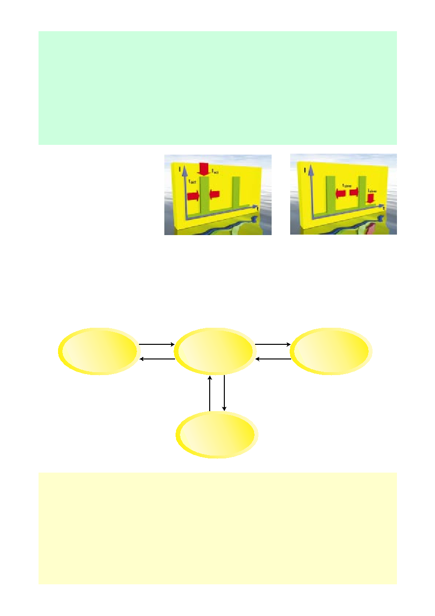
To reduce the current
consumption of a system,
the MSP430 allows
designers the ability to
influence the active cur-
rent consumption and
active time as well as
sleep mode current con-
sumption and sleep time.
The active mode cur-
rent consumption of the
MSP430 is 400 µA in a
typical 3-V system. The
time to wake-up from
the sleep mode to a total
functional system takes a
maximum of 6 µs. This
allows the MSP430 to be in sleep
modes longer and eliminates
unnecessary energy use in the
active mode. The powerful
16-bit CPU core ensures a fast
execution of the tasks
and
therefore reduces the active
time. This means that the higher
the performance of the CPU
core, the lower the system power
Second Quarter, 1999
A full range of MSP430
evaluation and support
tools are available
and provide easy-to-use
design solutions.
2
consumption. All MSP430 periph-
eral modules are specially
designed to support these ultra-
low power features.
The sleep modes offer a
reduced current consumption
even when some peripherals are
still active. For example, in a
simple real time clock (RTC), it
is not necessary to keep the
device in active mode. Another
example, the system can operate
from the 32-kHz (ACLK) clock
instead of 1-4 MHz (MCLK) with
the timers and LCD still active.
These examples are benefits of
the most often used low-power
mode 3 (LPM3) which consumes
1.3 µA typically. The current
consumption can be reduced
down to 0.1 µA in LPM4 where
the MSP430 is still capable of
processing external interrupts,
for example from a connected
keyboard. The sleep time can be
maximized due to the fast wake-
up from the low-power modes.
In a modern household, many electronic
applications like TV sets or stereo
systems are permanently in a standby
mode. Assuming the total standby power
in a household is 10 W, a country with 40
million households requires 400 MW just
to supply the standby energy. This
means that a mid sized power plant is
working only to supply the standby
energy for these parts.
The MSP430 is an ultra-low-power
microcontroller family and can help to
reduce this standby current. The typical
current consumption in low-power mode
is 1.3 µA, where the device is still capa-
ble of displaying information on the LCD
display or keeping a real-time clock
updated.
This ultra-low-power consumption is no
limitation for the outstanding high pro-
cessing capability. The 16-bit RISC CPU
core can perform tasks like calculation
of the energy, faster than conventional
4- and 8-bit microcontrollers.
This combination sets a new benchmark
of processing capability versus energy
consumption.
The MSP430 offers 1200 MIPS/Watt in
active mode. Finally, the high integration
of the MSP430 allows the user to build
up a system with a minimum of external
components. This leads to very cost
competitive system solutions.
The `Green' Microcontroller
Active Mode
550
µ
A with A/D
400
µ
A without A/D
CPU is active
Various modules are active
1-4 MHz on
LP-Mode LPM1 50
µ
A
CPU is inactive
Peripherals active
1-4 MHz on
LP-Mode LPM4 0.1
µ
A
CPU is inactive
Peripherals inactive
32 kHz off
wake up from LPM4 only with
external interrupt
all parameters typical at 3V
LP-Mode LPM3 1.3
µ
A
CPU is inactive
Peripherals active
32 kHz on
The MSP430 offers a variety of possibil-
ities to reduce the cost of the complete
system to a minimum.
∑ The use of the 32-kHz XTAL and the
internal DCO/FLL eliminates the need
for a second XTAL for the system fre-
quency. Furthermore, a ceramic res-
onator can be used in place of the
32-kHz XTAL; or, the system can be
operated without any external com-
ponent for the clock generation at all.
∑ The low-power features of the
MSP430 make it possible to choose a
smaller battery for the application
and still increase the system life due
to the various power saving modes.
∑ High code efficiency leads to smaller
memory sizes and drives cost down.
∑ The high integration of the device
makes an external LCD driver or an
external ADC unnecessary. This high
level of integration saves system
cost and lowers the failure rate of
the system by reducing the device
count.
∑ The ease-of-use MSP430 architec-
ture and the development tools
significantly improve the develop-
ment time and speed up the time-to-
market.
System Cost Saving with the MSP430 Family
Current consumption in active mode
Current consumption in sleep mode
3
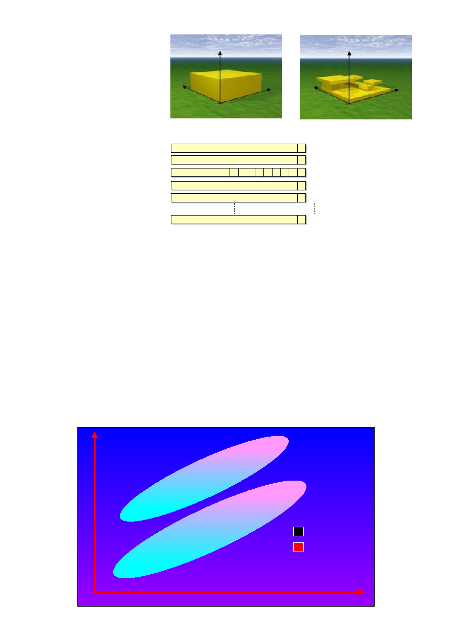
The MSP430 RISC Core
16-bit RISC CPU
The MSP430 CPU offers you
much more than standard 4- and
8-bit microcontrollers. The 16-bit
RISC core is built with a highly
orthogonal structure.
Every instruction can be used
with each of the seven different
addressing modes. The reduced
instruction set consists of only
27 core instructions. However,
the user has, due to the 24 addi-
tional emulated instructions the
capability of using highly famil-
iar instructions. For example, a
familiar instruction like INC R4
is available to the firmware pro-
grammer and automatically emu-
lated by the assembler with
ADD #1,R4. This instruction will
be executed like all other regis-
ter to register instructions in
only one cycle.
The orthogonal architecture
of the MSP430 CPU core makes
the device extremely easy-to-use.
Sixteen (16) registers are
implemented in the CPU itself
and contain the Program
counter, the stack pointer, the
Status Register and the Constant
Generator (which contains the
highly used constants -1, 0, 1, 2,
4 and 8). This feature makes the
MSP430 an extremely code effi-
cient device using a lot less of
the code space than convention-
al CISC machines. The remain-
ing 12 registers are available for
general usage.
0
0
0
0
0
R0, Program Counter PC
R1, Stack Pointer SP
R2, Status Register ST / Constant Generator CG
R3, Constant Generator CG
R4, General Purpose
R15, General Purpose
15
0
1
15
0
15
0
8
9
7
1
15
0
1
15
0
1
15
0
1
reserved for future enhancements
V
SCG1 SCG2
Osc
Off
CPU
Off
GIE
N
Z
C
Address
Modes Destination
Address
Modes Destination
Instructions
Instructions
Address Modes
Source
Example: orthogonality to operand
instructions
Example: non-orthogonality to operand
instructions
Address Modes
Source
Price
Complexity
Available
In Design
With LCD
Driver
Without LCD
Driver
x31x
CPU
Timer/Port
x32x
CPU
14-bit A/D
x33x
CPU
HW MPY +
UART
x11x
CPU
Timer_A
x11x1
CPU
Timer_A
Comparator_A
More
To
Come
The MSP430 Mixed-Signal Processor Roadmap
The hardware multiplication
module in the MSP430x33x con-
figuration provides multipli-
cations in less than one cycle.
The two operands are moved
into registers inside the multi-
plier module, and in the next
cycle, the result can be read out.
Oscillator / FLL Module
The clock network of the MSP430
offers the designer flexibility.
The Digital Controlled Oscillator
(DCO) generates the system
frequency of 1 to 4 MHz. The
32-kHz oscillator, which oper-
ates with only a single 32-kHz
crystal, can be used to provide a
stable frequency over tempera-
ture and operating voltage. The
integrated Frequency Locked
Loop (FLL) regulates the system
frequency MCLK with the stable
32-kHz crystal frequency. It is
even possible to operate the
MSP430 without any crystal at
all, disable the FLL and just use
the DCO to generate the system
clock.
The product offers a fail-safe
feature. If the crystal connection
is broken, the MSP430 continues
operation with the lowest possi-
ble frequency.
The DCO starts operation a
maximum of 6 µs after a reset or
interrupt occurs. This provides a
working system in a fraction of
the time needed with conven-
tional microcontrollers.
4
C=ROM, P=OTP, E=UV EPROM (prototyping only)
ADC: slope = slope measurements for resistive sensors, 14-bit = hardwired A/D converter with 14-bit resolution.
LCD = LCD Driver for 1-4 MUX, WDT = Watchdog Timer, BT = Basic Timer, T/P = Timer/Port Module, 8bT/C = 8-bit Timer/Counter, T_A = 16-bit Timer,
MPY = Hardware Multiplier, USART = UART/SPI, P0 ≠ P2 = I/O Ports.
^ If not used for LCD, the LCD segment lines can be used as outputs.
DEVICE
ROM
OTP
EPROM
RAM
ADC
LCD^
PERIPHERALS
PACKAGE
MSP430C111
2KB
128B
slope
N/A
WDT, P1, P2, T_A
20 SOP
MSP430C112
4KB
256B
slope
N/A
WDT, P1, P2, T_A
20 SOP
MSP430P112
4KB
256B
slope
N/A
WDT, P1, P2, T_A
20 SOP
PMS430E112
4KB
256B
slope
N/A
WDT, P1, P2, T_A
20 DIL
MSP430C311S
2KB
128B
slope
64seg
WDT, BT, T/P, P0, 8bT/C
48 SSOP
MSP430C312
4KB
256B
slope
92seg
WDT, BT, T/P, P0, 8bT/C
56 SSOP
MSP430C313
8KB
256B
slope
92seg
WDT, BT, T/P, P0, 8bT/C
56 SSOP
MSP430C314
12KB
512B
slope
92seg
WDT, BT, T/P, P0, 8bT/C
56 SSOP
MSP430C315
16KB
512B
slope
92seg
WDT, BT, T/P, P0, 8bT/C
56 SSOP
MSP430P313
8KB
256B
slope
92seg
WDT, BT, T/P, P0, 8bT/C
56 SSOP
PMS430E313
8KB
256B
slope
92seg
WDT, BT, T/P, P0, 8bT/C
68 CLCC
MSP430P315
16KB
512B
slope
92seg
WDT, BT, T/P, P0, 8bT/C
56 SSOP
MSP430P315S
16KB
512B
slope
64seg
WDT, BT, T/P, P0, 8bT/C
48 SSOP
PMS430E315
16KB
512B
slope
92seg
WDT, BT, T/P, P0, 8bT/C
68 CLCC
MSP430C323
8KB
256B
14 bit & slope
84seg
WDT, BT, T/P, P0, 8bT/C
64 QFP/68 PLCC
MSP430C325
16KB
512B
14 bit & slope
84seg
WDT, BT, T/P, P0, 8bT/C
64 QFP/68 PLCC
MSP430P325
16KB
512B
14 bit & slope
84seg
WDT, BT, T/P, P0, 8bT/C
64 QFP/68 PLCC
PMS430E325
16KB
512B
14 bit & slope
84seg
WDT, BT, T/P, P0, 8bT/C
68 CLCC
MSP430C336
24KB
1KB
slope
120seg
31x + T_A, MPY, USART, P1, P2, P3, P4
100 QFP
MSP430C337
32KB
1KB
slope
120seg
31x + T_A, MPY, USART, P1, P2, P3, P4
100 QFP
MSP430P337
32KB
1KB
slope
120seg
31x + T_A, MPY, USART, P1, P2, P3, P4
100 QFP
PMS430E337
32KB
1KB
slope
120seg
31x + T_A, MPY, USART, P1, P2, P3, P4
100 CQFP
MSP430 Mixed-Signal Processor Selection Guide
x31x
56 SSOP - DL
48 SSOP - DL
Timer/Port
x32x
64 QFP - PM (0.5 mm)
64 QFP - PG (1 mm)
68 PLCC - FN
ADC 14 bit
x33x
100 QFP - PJM
H/W Multiplier
16-bit Timer, USART
x11x
20 SOP - DW
Timer_A
32 KB
24 KB
16 KB
12 KB
8 KB
4 KB
2 KB
C111
C311S
C312
C313
C314
P315
P315S
C325
C323
P325
C337
P337
C315
P313
C112
C336
P112
The MSP430 Mixed-Signal Processor Family
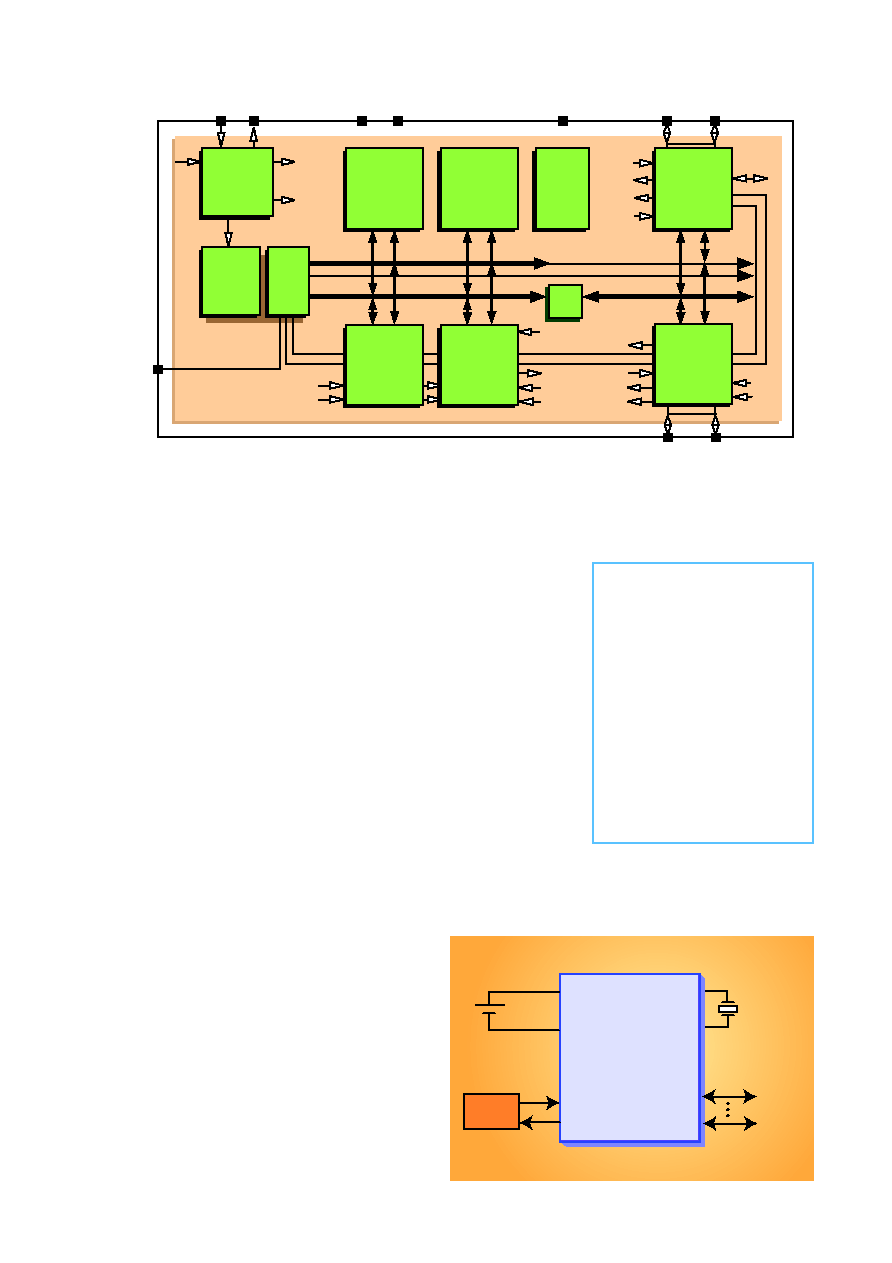
The MSP430 family offers you flexibility. Choose from several members out of four configurations:
∑ MSP430x11x devices ≠ Basic version with Timer_A
∑ MSP430x31x devices ≠ A/D conversion with the Timer/Port module
∑ MSP430x32x devices ≠ A/D conversion with 14-bit ADC module
∑ MSP430x33x devices ≠ High-end version with Timer_A, USART and H/W multiplier
5
MSP430x11x Configuration
The newest member in the
MSP430 microcontroller family
offers an unmatched ratio of
ultra-low power consumption,
16-bit RISC performance, and
low cost. The MSP430x11x
family features an ultra-low
power consumption rating of
350 µA in active mode, 1.5 µA in
standby mode and 0.1 µA in
(RAM-retention) off mode. With
volume pricing as low as $1 for
ROM versions, the 11x devices
are quickly becoming the bench-
mark in this price/performance
range.
The 16-bit RISC core operates
up to 5 MHz, allowing most of
the 27 core instructions to be
executed within one 200-ns
cycle. This combination of 27
core instructions and the orthog-
onal architecture allows every
instruction to be used in each
addressing mode, making the
MSP430x11x easy to program.
It's also completely code com-
patible with TI's other MSP430
families.
Among the peripherals inte-
grated into the new device are:
a 16-bit timer with three capture/
compare, 14 individual I/O signals,
a new basic clock system, watch-
dog timer and JTAG interface.
The new basic clock system
makes it possible to increase
the maximum standby time to
128 seconds. The memory sizes
are 2 or 4 KB with the ROM
version and 4 KB with the low-
power OTP version. The OTP
version (MSP430P112IDW) is
available now.
2/4 KB ROM
128/256B
RAM
SRAM
Power
On
Reset
JTAG
Bus
conv.
4 KB OTP
'C' ROM
'P' OTP
'E' EPROM
CPU
incl. 16 reg.
Rosc
X
IN
TEST/VPP
MAB, 16 bit
MDB, 16 bit
MAB, 4 bit
MCB
MDB, 8 bit
X
OUT
ACLK
MCLK
ACLK
SMCLK
SMCLK
V
CC
V
SS
RST/NMI
P1.0
P1.7
P2.0
P2.5
I/O port 2
6 I/Os, all
with interr.
capability
Watchdog
Timer
15 bit
Timer_A
3 CC Register
CCR0/1/2
x = 0, 1, 2
Test
JTAG
Oscillator
System
Clock
I/O port 1
8 I/Os, all
with interr.
capability
Outx
CCIxA
CCIxB
Out0
CCI0B
CCI1B
DCOR
ACLK
Outx
CCIxA
TACLK
SMCLK
TACLK or INCLK
INCLK
MSP430x11x Application Example
The MSP430x11x series, new members to the
MSP430 family, expands the reach of low-cost
system design to a higher level. A 10-year Real-Time
Clock is one of many system applications that
minimize the cost to manufacturers while simplify
the design and development cycle drastically.
Working at Low Power Mode 3 (LPM3), the
MSP430x11x receives the time input from a 32,768-Hz
external crystal oscillator. With a connection to an
outside host device through UART or SPI port,
MSP430x11x internally generates a timer interrupt
service routine to wake-up once per second. System
integration engineers will be able to develop an
application specific system by taking advantage of
this 1.52-µA average current consumption solution.
TX
Xin
Xout
RX
P2.x
P1.x
V
SS
V
CC
32768
12 Pins
for
Expansion
MSP430C111
3V
Host
UART, SPI, IIC
Low-cost 10-year Real-Time Clock (RTC)
Typical applications
The MSP430x11x is ideally suited for
portable instrumentation equipment
such as:
∑ Real-time clock
∑ Communication
∑ Digital motor control
∑ Home automation
∑ Alarm systems
∑ Data loggers
Development tools
Development tools for the MSP430x11x
include an Evaluation Kit from TI,
and in-circuit emulators and C-
Compilers are available from third-
party development tool vendors.