Document Outline
- features
- description
- pin designation, MSP430F133, MSP430F135
- pin designation, MSP430F147, MSP430F148, MSP430F149
- pin designation, MSP430F1471, MSP430F1481, MSP430F1491
- functional block diagrams
- MSP430x13x
- MSP430x14x
- MSP430x14x1
- Terminal Functions
- MSP430x13x, MSP430x14x
- MSP430x14x1
- short-form description
- CPU
- instruction set
- operating modes
- interrupt vector addresses
- special function registers
- interrupt enable 1 and 2
- interrupt flag register 1 and 2
- module enable registers 1 and 2
- memory organization
- bootstrap loader (BSL)
- flash memory
- peripherals
- digital I/O
- oscillator and system clock
- watchdog timer
- hardware multiplier (MSP430x14x and MSP430x14x1 Only)
- USART0
- USART1 (MSP430x14x and MSP430x14x1 Only)
- comparator_A
- ADC12 (Not implemented in the MSP430x14x1)
- timer_A3
- timer_B3 (MSP430x13x Only)
- timer_B7 (MSP430x14x and MSP430x14x1 Only)
- peripheral file map
- absolute maximum ratings over operating free-air temperature (unless otherwise noted)Å
- recommended operating conditions
- electrical characteristics over recommended operating free-air temperature (unless otherwise noted)
- supply current into AVCC + DVCC excluding external current
- SCHMITT-trigger inputs - Ports P1, P2, P3, P4, P5, and P6
- standard inputs - RST\/NMI; JTAG: TCK, TMS, TDI/TCLK, TDO/TDI
- inputs Px.x, TAx, TBx
- leakage current (see Note 1)
- outputs - Ports P1, P2, P3, P4, P5, and P6
- output frequency
- wake-up LPM3
- RAM
- Comparator_A (see Note 1)
- PUC/POR
- DCO (see Note 1)
- main DCO characteristics
- DCO when using ROSC ( see Note 1)
- crystal oscillator, LFXT1 oscillator (see Note 1)
- crystal oscillator, XT2 oscillator (see Note 1)
- USART0, USART1 (see Note 1)
- 12-bit ADC, power supply and input range conditions (see Note 1)
- 12-bit ADC, external reference (see Note 1)
- 12-bit ADC, built-in reference
- 12-bit ADC, timing parameters
- 12-bit ADC, linearity parameters
- 12-bit ADC, temperature sensor and built-in VMID
- Flash Memory
- JTAG Interface
- JTAG Fuse (see Note 1)
- APPLICATION INFORMATION
- input/output schematic
- port P1, P1.0 to P1.7, input/output with Schmitt-trigger
- port P2, P2.0 to P2.2, P2.6, and P2.7 input/output with Schmitt-trigger
- port P2, P2.3 to P2.4, input/output with Schmitt-trigger
- port P2, P2.5, input/output with Schmitt-trigger and Rosc function for the basic clock module
- port P3, P3.0 and P3.4 to P3.7, input/output with Schmitt-trigger
- port P3, P3.1, input/output with Schmitt-trigger
- port P3, P3.2, input/output with Schmitt-trigger
- port P3, P3.3, input/output with Schmitt-trigger
- port P4, P4.0 to P4.6, input/output with Schmitt-trigger
- port P4, P4.7, input/output with Schmitt-trigger
- port P5, P5.0 and P5.4 to P5.7, input/output with Schmitt-trigger
- port P5, P5.1, input/output with Schmitt-trigger
- port P5, P5.2, input/output with Schmitt-trigger
- port P5, P5.3, input/output with Schmitt-trigger
- port P6, P6.0 to P6.7, input/output with Schmitt-trigger
- JTAG pins TMS, TCK, TDI/TCLK, TDO/TDI, input/output with Schmitt-trigger
- JTAG fuse check mode
- THERMAL MECHANICAL DATA
- RTD (S0PQFP-N64) PLASTIC QUAD FLATPACK
- MECHANICAL DATA
- RTD (S-PQFP-N64) PLASTIC QUAD FLATPACK

MSP430x13x, MSP430x14x, MSP430x14x1
MIXED SIGNAL MICROCONTROLLER
SLAS272F - JULY 2000 - REVISED JUNE 2004
1
POST OFFICE BOX 655303
∑
DALLAS, TEXAS 75265
D
Low Supply-Voltage Range, 1.8 V . . . 3.6 V
D
Ultralow-Power Consumption:
- Active Mode: 280
µ
A at 1 MHz, 2.2V
- Standby Mode: 1.6
µ
A
- Off Mode (RAM Retention): 0.1
µ
A
D
Five Power-Saving Modes
D
Wake-Up From Standby Mode in less
than 6
µ
s
D
16-Bit RISC Architecture,
125-ns Instruction Cycle Time
D
12-Bit A/D Converter With Internal
Reference, Sample-and-Hold and Autoscan
Feature
D
16-Bit Timer_B With Seven
Capture/Compare-With-Shadow Registers
D
16-Bit Timer_A With Three
Capture/Compare Registers
D
On-Chip Comparator
D
Serial Onboard Programming,
No External Programming Voltage Needed
Programmable Code Protection by Security
Fuse
D
Serial Communication Interface (USART),
Functions as Asynchronous UART or
Synchronous SPI Interface
- Two USARTs (USART0, USART1) --
MSP430x14x(1) Devices
- One USART (USART0) -- MSP430x13x
Devices
D
Family Members Include:
- MSP430F133:
8KB+256B Flash Memory,
256B RAM
- MSP430F135:
16KB+256B Flash Memory,
512B RAM
- MSP430F147, MSP430F1471
:
32KB+256B Flash Memory,
1KB RAM
- MSP430F148, MSP430F1481
:
48KB+256B Flash Memory,
2KB RAM
- MSP430F149, MSP430F1491
:
60KB+256B Flash Memory,
2KB RAM
D
Available in 64-Pin Quad Flat Pack (QFP)
and 64-pin QFN
D
For Complete Module Descriptions, See the
MSP430x1xx Family User's Guide,
Literature Number SLAU049
The MSP430F14x1 devices are identical to the MSP430F14x
devices with the exception that the ADC12 module is not
implemented.
description
The Texas Instruments MSP430 family of ultralow-power microcontrollers consist of several devices featuring
different sets of peripherals targeted for various applications. The architecture, combined with five low power
modes is optimized to achieve extended battery life in portable measurement applications. The device features
a powerful 16-bit RISC CPU, 16-bit registers, and constant generators that attribute to maximum code efficiency.
The digitally controlled oscillator (DCO) allows wake-up from low-power modes to active mode in less than 6
µ
s.
The MSP430x13x and the MSP430x14x(1) series are microcontroller configurations with two built-in 16-bit
timers, a fast 12-bit A/D converter (not implemented on the MSP430F14x1 devices), one or two universal serial
synchronous/asynchronous communication interfaces (USART), and 48 I/O pins.
Typical applications include sensor systems that capture analog signals, convert them to digital values, and
process and transmit the data to a host system. The timers make the configurations ideal for industrial control
applications such as ripple counters, digital motor control, EE-meters, hand-held meters, etc. The hardware
multiplier enhances the performance and offers a broad code and hardware-compatible family solution.
Copyright
2000 - 2004, Texas Instruments Incorporated
PRODUCTION DATA information is current as of publication date.
Products conform to specifications per the terms of Texas Instruments
standard warranty. Production processing does not necessarily include
testing of all parameters.
Please be aware that an important notice concerning availability, standard warranty, and use in critical applications of
Texas Instruments semiconductor products and disclaimers thereto appears at the end of this data sheet.
MSP430x13x, MSP430x14x, MSP430x14x1
MIXED SIGNAL MICROCONTROLLER
SLAS272F - JULY 2000 - REVISED JUNE 2004
2
POST OFFICE BOX 655303
∑
DALLAS, TEXAS 75265
AVAILABLE OPTIONS
PACKAGED DEVICES
TA
PLASTIC 64-PIN QFP
(PM)
PLASTIC 64-PIN QFP
(PAG)
PLASTIC 64-PIN QFN
(RTD)
-40
∞
C to 85
∞
C
MSP430F133IPM
MSP430F135IPM
MSP430F147IPM
MSP430F1471IPM
MSP430F148IPM
MSP430F1481IPM
MSP430F149IPM
MSP430F1491IPM
MSP430F133IPAG
MSP430F135IPAG
MSP430F147IPAG
MSP430F148IPAG
MSP430F149IPAG
MSP430F133IRTD
MSP430F135IRTD
MSP430F147IRTD
MSP430F1471IRTD
MSP430F148IRTD
MSP430F1481IRTD
MSP430F149IRTD
MSP430F1491IRTD
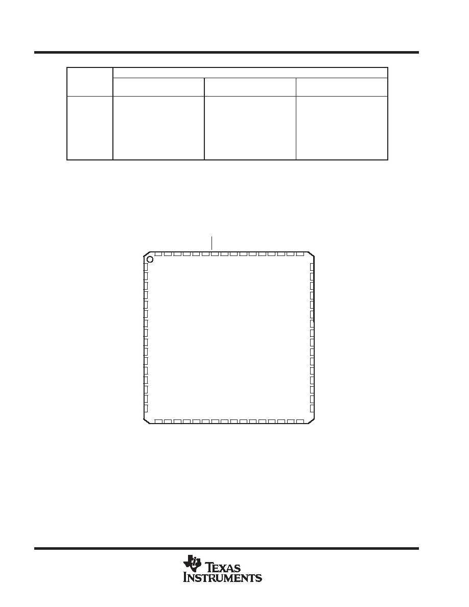
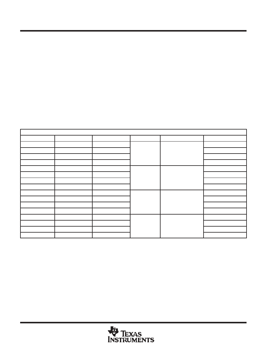
pin designation, MSP430F133, MSP430F135
17 18 19
P5.4/MCLK
P5.3
P5.2
P5.1
P5.0
P4.7/TBCLK
P4.6
P4.5
P4.4
P4.3
P4.2/TB2
P4.1/TB1
P4.0/TB0
P3.7
P3.6
P3.5/URXD0
48
47
46
45
44
43
42
41
40
39
38
37
36
35
34
33
20
1
2
3
4
5
6
7
8
9
10
11
12
13
14
15
16
DV
CC
P6.3/A3
P6.4/A4
P6.5/A5
P6.6/A6
P6.7/A7
V
REF+
XIN
XOUT
Ve
REF+
V
REF-
/Ve
REF-
P1.0/TACLK
P1.1/TA0
P1.2/TA1
P1.3/TA2
P1.4/SMCLK
21 22 23 24
P5.6/ACLK
TDO/TDI
63 62 61 60 59
64
58
AV
P6.2/A2
P6.1/A1
P6.0/A0
RST/NMI
TCK
TMS
P2.6/ADC12CLK
P2.7/T
A0
P3.0/STE0
P3.1/SIMO0
P1.7/T
A2
P2.1/T
AINCLK
P2.2/CAOUT/T
A0
P2.3/CA0/T
A1
P2.4/CA1/T
A2
P2.5/Rosc
56 55 54
57
25 26 27 28 29
53 52
P1.5/T
A0
XT2IN
XT2OUT
51 50 49
30 31 32
P3.2/SOMI0
P3.3/UCLK0
P3.4/UTXD0
P5.7/TBOUTH
TDI/TCLK
P5.5/SMCLK
AV
DV
PM, PAG, RTD PACKAGE
(TOP VIEW)
P1.6/T
A1
P2.0/ACLK
CC
SS
SS
MSP430x13x, MSP430x14x, MSP430x14x1
MIXED SIGNAL MICROCONTROLLER
SLAS272F - JULY 2000 - REVISED JUNE 2004
3
POST OFFICE BOX 655303
∑
DALLAS, TEXAS 75265
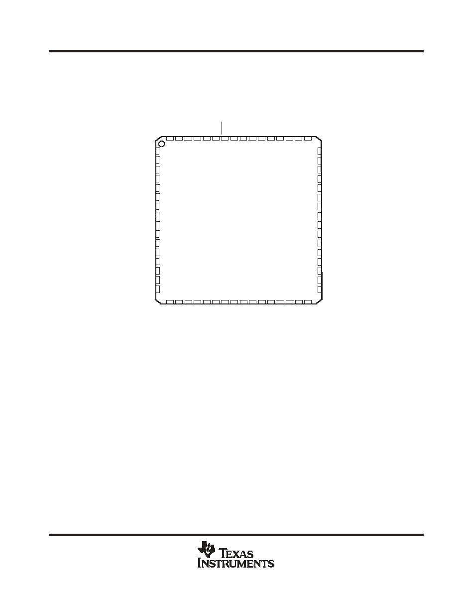
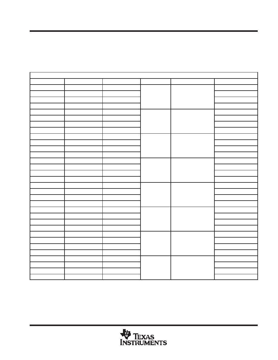
pin designation, MSP430F147, MSP430F148, MSP430F149
17 18 19
P5.4/MCLK
P5.3/UCLK1
P5.2/SOMI1
P5.1/SIMO1
P5.0/STE1
P4.7/TBCLK
P4.6/TB6
P4.5/TB5
P4.4/TB4
P4.3/TB3
P4.2/TB2
P4.1/TB1
P4.0/TB0
P3.7/URXD1
P3.6/UTXD1
P3.5/URXD0
48
47
46
45
44
43
42
41
40
39
38
37
36
35
34
33
20
1
2
3
4
5
6
7
8
9
10
11
12
13
14
15
16
DV
CC
P6.3/A3
P6.4/A4
P6.5/A5
P6.6/A6
P6.7/A7
V
REF+
XIN
XOUT
Ve
REF+
V
REF-
/Ve
REF-
P1.0/TACLK
P1.1/TA0
P1.2/TA1
P1.3/TA2
P1.4/SMCLK
21 22 23 24
P5.6/ACLK
TDO/TDI
63 62 61 60 59
64
58
AV
P6.2/A2
P6.1/A1
P6.0/A0
RST/NMI
TCK
TMS
P2.6/ADC12CLK
P2.7/T
A0
P3.0/STE0
P3.1/SIMO0
P1.7/T
A2
P2.1/T
AINCLK
P2.2/CAOUT/T
A0
P2.3/CA0/T
A1
P2.4/CA1/T
A2
P2.5/Rosc
56 55 54
57
25 26 27 28 29
53 52
P1.5/T
A0
XT2IN
XT2OUT
51 50 49
30 31 32
P3.2/SOMI0
P3.3/UCLK0
P3.4/UTXD0
P5.7/TBOUTH
TDI/TCLK
P5.5/SMCLK
AV
DV
PM, PAG, RTD PACKAGE
(TOP VIEW)
P1.6/T
A1
P2.0/ACLK
CC
SS
SS
MSP430x13x, MSP430x14x, MSP430x14x1
MIXED SIGNAL MICROCONTROLLER
SLAS272F - JULY 2000 - REVISED JUNE 2004
4
POST OFFICE BOX 655303
∑
DALLAS, TEXAS 75265
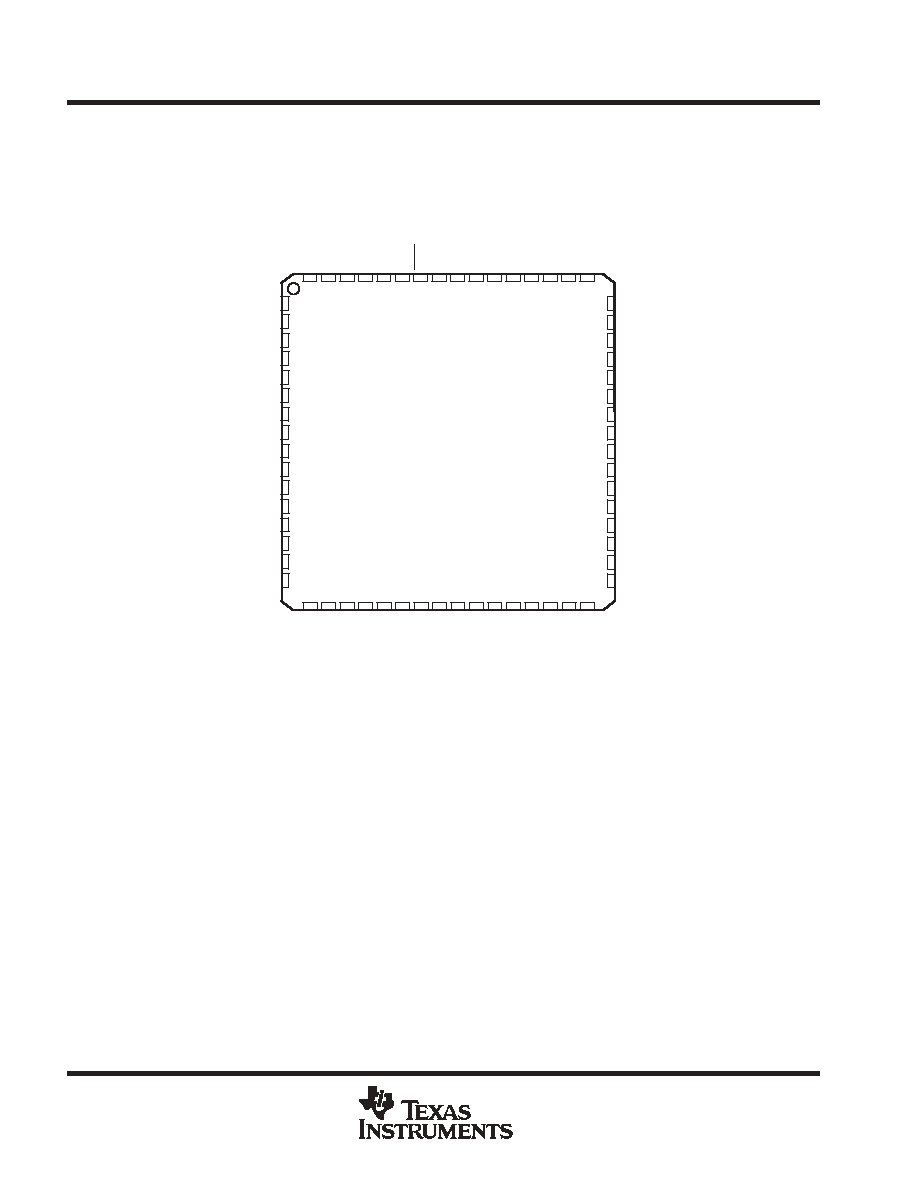
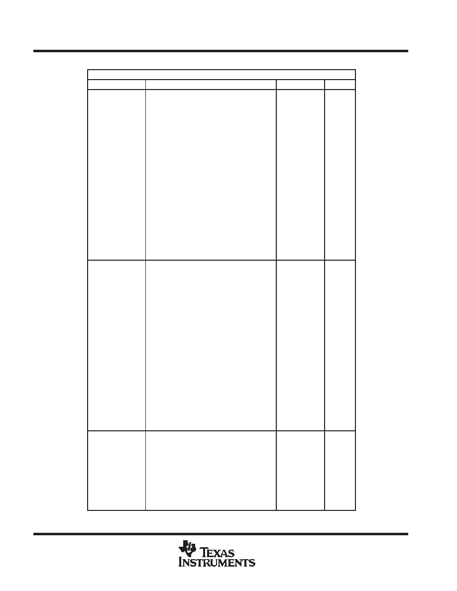
pin designation, MSP430F1471, MSP430F1481, MSP430F1491
17 18 19
P5.4/MCLK
P5.3/UCLK1
P5.2/SOMI1
P5.1/SIMO1
P5.0/STE1
P4.7/TBCLK
P4.6/TB6
P4.5/TB5
P4.4/TB4
P4.3/TB3
P4.2/TB2
P4.1/TB1
P4.0/TB0
P3.7/URXD1
P3.6/UTXD1
P3.5/URXD0
48
47
46
45
44
43
42
41
40
39
38
37
36
35
34
33
20
1
2
3
4
5
6
7
8
9
10
11
12
13
14
15
16
DV
CC
P6.3
P6.4
P6.5
P6.6
P6.7
Reserved
XIN
XOUT
DV
SS
DV
SS
P1.0/TACLK
P1.1/TA0
P1.2/TA1
P1.3/TA2
P1.4/SMCLK
21 22 23 24
P5.6/ACLK
TDO/TDI
63 62 61 60 59
64
58
AV
P6.2
P6.1
P6.0
RST/NMI
TCK
TMS
P2.6
P2.7/T
A0
P3.0/STE0
P3.1/SIMO0
P1.7/T
A2
P2.1/T
AINCLK
P2.2/CAOUT/T
A0
P2.3/CA0/T
A1
P2.4/CA1/T
A2
P2.5/Rosc
56 55 54
57
25 26 27 28 29
53 52
P1.5/T
A0
XT2IN
XT2OUT
51 50 49
30 31 32
P3.2/SOMI0
P3.3/UCLK0
P3.4/UTXD0
P5.7/TBOUTH
TDI/TCLK
P5.5/SMCLK
AV
DV
PM, RTD PACKAGE
(TOP VIEW)
P1.6/T
A1
P2.0/ACLK
CC
SS
SS
MSP430x13x, MSP430x14x, MSP430x14x1
MIXED SIGNAL MICROCONTROLLER
SLAS272F - JULY 2000 - REVISED JUNE 2004
5
POST OFFICE BOX 655303
∑
DALLAS, TEXAS 75265
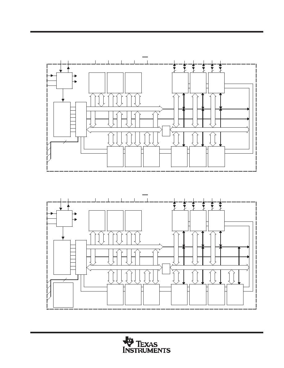
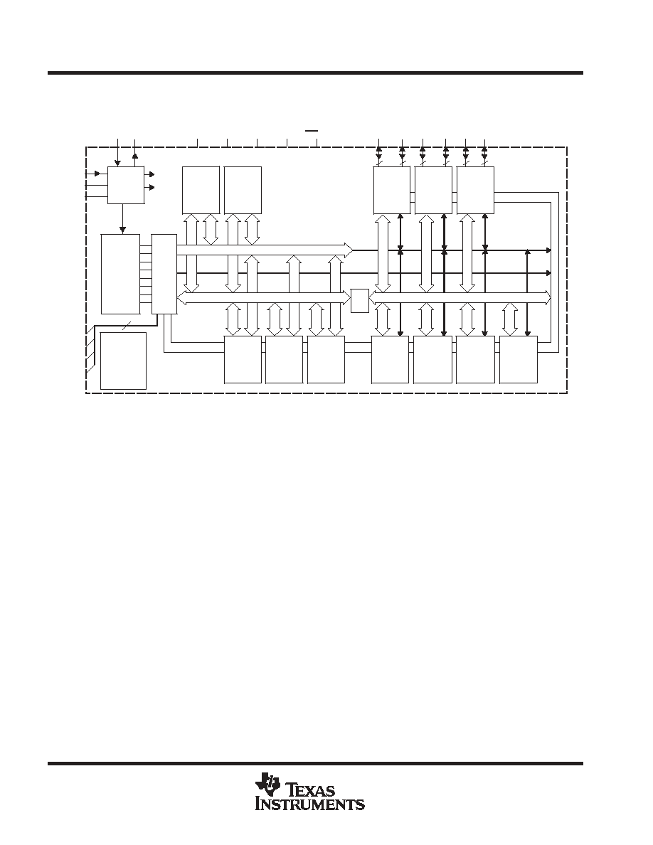
functional block diagrams
MSP430x13x
Oscillator
ACLK
SMCLK
CPU
Incl. 16 Reg.
Bus
Conv
MCB
XIN
XOUT
P3
P4
P2
XT2IN
XT2OUT
TMS
TCK
MDB, 16 Bit
MAB, 16 Bit
MCLK
4
TDI/TCLK
TDO/TDI
P5
P6
MAB,
4 Bit
DVCC
DVSS
AVCC
AVSS RST/NMI
System
Clock
ROSC
P1
16KB Flash
8KB Flash
512B RAM
256B RAM
ADC12
12-Bit
8 Channels
<10
µ
s Conv.
Watchdog
Timer
15/16-Bit
Timer_B3
3 CC Reg
Shadow
Reg
Timer_A3
3 CC Reg
Test
JTAG
Emulation
Module
I/O Port 1/2
16 I/Os,
with
Interrupt
Capability
I/O Port 3/4
16 I/Os
POR
Comparator
A
USART0
UART Mode
SPI Mode
I/O Port 5/6
16 I/Os
MDB, 8 Bit
MDB, 16-Bit
MAB, 16-Bit
8
8
8
8
8
8
MSP430x14x
Oscillator
ACLK
SMCLK
CPU
Incl. 16 Reg.
Bus
Conv
MCB
XIN
XOUT
P3
P4
P2
XT2IN
XT2OUT
TMS
TCK
MDB, 16 Bit
MAB, 16 Bit
MCLK
4
TDI/TCLK
TDO/TDI
P5
P6
MAB,
4 Bit
DVCC
DVSS
AVCC
AVSS RST/NMI
System
Clock
ROSC
P1
Hardware
Multiplier
MPY, MPYS
MAC,MACS
60KB Flash
48KB Flash
32KB Flash
2KB RAM
2KB RAM
1KB RAM
ADC12
12-Bit
8 Channels
<10
µ
s Conv.
Watchdog
Timer
15/16-Bit
Timer_B7
7 CC Reg
Shadow
Reg
Timer_A3
3 CC Reg
Test
JTAG
Emulation
Module
I/O Port 1/2
16 I/Os,
with
Interrupt
Capability
I/O Port 3/4
16 I/Os
POR
Comparator
A
USART0
UART Mode
SPI Mode
USART1
UART Mode
SPI Mode
I/O Port 5/6
16 I/Os
MDB, 8 Bit
MDB, 16-Bit
MAB, 16-Bit
8
8
8
8
8
8
MSP430x13x, MSP430x14x, MSP430x14x1
MIXED SIGNAL MICROCONTROLLER
SLAS272F - JULY 2000 - REVISED JUNE 2004
6
POST OFFICE BOX 655303
∑
DALLAS, TEXAS 75265
functional block diagrams (continued)
MSP430x14x1
Oscillator
ACLK
SMCLK
CPU
Incl. 16 Reg.
Bus
Conv
MCB
XIN
XOUT
P3
P4
P2
XT2IN
XT2OUT
TMS
TCK
MDB, 16 Bit
MAB, 16 Bit
MCLK
4
TDI/TCLK
TDO/TDI
P5
P6
MAB,
4 Bit
DVCC
DVSS
AVCC
AVSS RST/NMI
System
Clock
ROSC
P1
Hardware
Multiplier
MPY, MPYS
MAC,MACS
60KB Flash
48KB Flash
32KB Flash
2KB RAM
2KB RAM
1KB RAM
Watchdog
Timer
15/16-Bit
Timer_B7
7 CC Reg
Shadow
Reg
Timer_A3
3 CC Reg
Test
JTAG
Emulation
Module
I/O Port 1/2
16 I/Os,
with
Interrupt
Capability
I/O Port 3/4
16 I/Os
POR
Comparator
A
USART0
UART Mode
SPI Mode
USART1
UART Mode
SPI Mode
I/O Port 5/6
16 I/Os
MDB, 8 Bit
MDB, 16-Bit
MAB, 16-Bit
8
8
8
8
8
8
MSP430x13x, MSP430x14x, MSP430x14x1
MIXED SIGNAL MICROCONTROLLER
SLAS272F - JULY 2000 - REVISED JUNE 2004
7
POST OFFICE BOX 655303
∑
DALLAS, TEXAS 75265
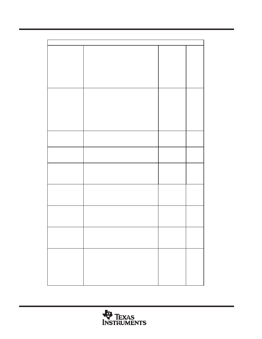
Terminal Functions
MSP430x13x, MSP430x14x
TERMINAL
I/O
DESCRIPTION
NAME
NO.
I/O
DESCRIPTION
AVCC
64
Analog supply voltage, positive terminal. Supplies the analog portion of the analog-to-digital converter.
AVSS
62
Analog supply voltage, negative terminal. Supplies the analog portion of the analog-to-digital converter.
DVCC
1
Digital supply voltage, positive terminal. Supplies all digital parts.
DVSS
63
Digital supply voltage, negative terminal. Supplies all digital parts.
P1.0/TACLK
12
I/O
General-purpose digital I/O pin/Timer_A, clock signal TACLK input
P1.1/TA0
13
I/O
General-purpose digital I/O pin/Timer_A, capture: CCI0A input, compare: Out0 output/BSL transmit
P1.2/TA1
14
I/O
General-purpose digital I/O pin/Timer_A, capture: CCI1A input, compare: Out1 output
P1.3/TA2
15
I/O
General-purpose digital I/O pin/Timer_A, capture: CCI2A input, compare: Out2 output
P1.4/SMCLK
16
I/O
General-purpose digital I/O pin/SMCLK signal output
P1.5/TA0
17
I/O
General-purpose digital I/O pin/Timer_A, compare: Out0 output
P1.6/TA1
18
I/O
General-purpose digital I/O pin/Timer_A, compare: Out1 output
P1.7/TA2
19
I/O
General-purpose digital I/O pin/Timer_A, compare: Out2 output/
P2.0/ACLK
20
I/O
General-purpose digital I/O pin/ACLK output
P2.1/TAINCLK
21
I/O
General-purpose digital I/O pin/Timer_A, clock signal at INCLK
P2.2/CAOUT/TA0
22
I/O
General-purpose digital I/O pin/Timer_A, capture: CCI0B input/Comparator_A output/BSL receive
P2.3/CA0/TA1
23
I/O
General-purpose digital I/O pin/Timer_A, compare: Out1 output/Comparator_A input
P2.4/CA1/TA2
24
I/O
General-purpose digital I/O pin/Timer_A, compare: Out2 output/Comparator_A input
P2.5/ROSC
25
I/O
General-purpose digital I/O pin/input for external resistor defining the DCO nominal frequency
P2.6/ADC12CLK
26
I/O
General-purpose digital I/O pin/conversion clock ≠ 12-bit ADC
P2.7/TA0
27
I/O
General-purpose digital I/O pin/Timer_A, compare: Out0 output
P3.0/STE0
28
I/O
General-purpose digital I/O pin/slave transmit enable ≠ USART0/SPI mode
P3.1/SIMO0
29
I/O
General-purpose digital I/O pin/slave in/master out of USART0/SPI mode
P3.2/SOMI0
30
I/O
General-purpose digital I/O pin/slave out/master in of USART0/SPI mode
P3.3/UCLK0
31
I/O
General-purpose digital I/O/USART0 clock: external input - UART or SPI mode, output ≠ SPI mode
P3.4/UTXD0
32
I/O
General-purpose digital I/O pin/transmit data out ≠ USART0/UART mode
P3.5/URXD0
33
I/O
General-purpose digital I/O pin/receive data in ≠ USART0/UART mode
P3.6/UTXD1
34
I/O
General-purpose digital I/O pin/transmit data out ≠ USART1/UART mode
P3.7/URXD1
35
I/O
General-purpose digital I/O pin/receive data in ≠ USART1/UART mode
P4.0/TB0
36
I/O
General-purpose digital I/O pin/Timer_B, capture: CCI0A or CCI0B input, compare: Out0 output
P4.1/TB1
37
I/O
General-purpose digital I/O pin/Timer_B, capture: CCI1A or CCI1B input, compare: Out1 output
P4.2/TB2
38
I/O
General-purpose digital I/O pin/Timer_B, capture: CCI2A or CCI2B input, compare: Out2 output
P4.3/TB3
39
I/O
General-purpose digital I/O pin/Timer_B, capture: CCI3A or CCI3B input, compare: Out3 output
P4.4/TB4
40
I/O
General-purpose digital I/O pin/Timer_B, capture: CCI4A or CCI4B input, compare: Out4 output
P4.5/TB5
41
I/O
General-purpose digital I/O pin/Timer_B, capture: CCI5A or CCI5B input, compare: Out5 output
P4.6/TB6
42
I/O
General-purpose digital I/O pin/Timer_B, capture: CCI6A or CCI6B input, compare: Out6 output
P4.7/TBCLK
43
I/O
General-purpose digital I/O pin/Timer_B, clock signal TBCLK input
P5.0/STE1
44
I/O
General-purpose digital I/O pin/slave transmit enable ≠ USART1/SPI mode
P5.1/SIMO1
45
I/O
General-purpose digital I/O pin/slave in/master out of USART1/SPI mode
P5.2/SOMI1
46
I/O
General-purpose digital I/O pin/slave out/master in of USART1/SPI mode
P5.3/UCLK1
47
I/O
General-purpose digital I/O pin/USART1 clock: external input - UART or SPI mode, output ≠ SPI mode
P5.4/MCLK
48
I/O
General-purpose digital I/O pin/main system clock MCLK output
P5.5/SMCLK
49
I/O
General-purpose digital I/O pin/submain system clock SMCLK output
14x devices only
MSP430x13x, MSP430x14x, MSP430x14x1
MIXED SIGNAL MICROCONTROLLER
SLAS272F - JULY 2000 - REVISED JUNE 2004
8
POST OFFICE BOX 655303
∑
DALLAS, TEXAS 75265
Terminal Functions (Continued)
MSP430x13x, MSP430x14x (continued)
TERMINAL
I/O
DESCRIPTION
NAME
NO.
I/O
DESCRIPTION
P5.6/ACLK
50
I/O
General-purpose digital I/O pin/auxiliary clock ACLK output
P5.7/TBOUTH
51
I/O
General-purpose digital I/O pin/switch all PWM digital output ports to high impedance - Timer_B7: TB0 to
TB6
P6.0/A0
59
I/O
General-purpose digital I/O pin/analog input a0 ≠ 12-bit ADC
P6.1/A1
60
I/O
General-purpose digital I/O pin/analog input a1 ≠ 12-bit ADC
P6.2/A2
61
I/O
General-purpose digital I/O pin/analog input a2 ≠ 12-bit ADC
P6.3/A3
2
I/O
General-purpose digital I/O pin/analog input a3 ≠ 12-bit ADC
P6.4/A4
3
I/O
General-purpose digital I/O pin/analog input a4 ≠ 12-bit ADC
P6.5/A5
4
I/O
General-purpose digital I/O pin/analog input a5 ≠ 12-bit ADC
P6.6/A6
5
I/O
General-purpose digital I/O pin/analog input a6 ≠ 12-bit ADC
P6.7/A7
6
I/O
General-purpose digital I/O pin/analog input a7 ≠ 12-bit ADC
RST/NMI
58
I
Reset input, nonmaskable interrupt input port, or bootstrap loader start (in Flash devices).
TCK
57
I
Test clock. TCK is the clock input port for device programming test and bootstrap loader start (in Flash
devices).
TDI/TCLK
55
I
Test data input or test clock input. The device protection fuse is connected to TDI/TCLK.
TDO/TDI
54
I/O
Test data output port. TDO/TDI data output or programming data input terminal
TMS
56
I
Test mode select. TMS is used as an input port for device programming and test.
VeREF+
10
I
Input for an external reference voltage to the ADC
VREF+
7
O
Output of positive terminal of the reference voltage in the ADC
VREF-/VeREF-
11
I
Negative terminal for the ADC's reference voltage for both sources, the internal reference voltage, or an
external applied reference voltage
XIN
8
I
Input port for crystal oscillator XT1. Standard or watch crystals can be connected.
XOUT
9
O
Output terminal of crystal oscillator XT1
XT2IN
53
I
Input port for crystal oscillator XT2. Only standard crystals can be connected.
XT2OUT
52
O
Output terminal of crystal oscillator XT2
QFN Pad
NA
NA
QFN package pad connection to DVSS recommended.

MSP430x13x, MSP430x14x, MSP430x14x1
MIXED SIGNAL MICROCONTROLLER
SLAS272F - JULY 2000 - REVISED JUNE 2004
9
POST OFFICE BOX 655303
∑
DALLAS, TEXAS 75265
Terminal Functions
MSP430x14x1
TERMINAL
I/O
DESCRIPTION
NAME
NO.
I/O
DESCRIPTION
AVCC
64
Analog supply voltage, positive terminal.
AVSS
62
Analog supply voltage, negative terminal.
DVCC
1
Digital supply voltage, positive terminal. Supplies all digital parts.
DVSS
63
Digital supply voltage, negative terminal. Supplies all digital parts.
P1.0/TACLK
12
I/O
General-purpose digital I/O pin/Timer_A, clock signal TACLK input
P1.1/TA0
13
I/O
General-purpose digital I/O pin/Timer_A, capture: CCI0A input, compare: Out0 output/BSL transmit
P1.2/TA1
14
I/O
General-purpose digital I/O pin/Timer_A, capture: CCI1A input, compare: Out1 output
P1.3/TA2
15
I/O
General-purpose digital I/O pin/Timer_A, capture: CCI2A input, compare: Out2 output
P1.4/SMCLK
16
I/O
General-purpose digital I/O pin/SMCLK signal output
P1.5/TA0
17
I/O
General-purpose digital I/O pin/Timer_A, compare: Out0 output
P1.6/TA1
18
I/O
General-purpose digital I/O pin/Timer_A, compare: Out1 output
P1.7/TA2
19
I/O
General-purpose digital I/O pin/Timer_A, compare: Out2 output
P2.0/ACLK
20
I/O
General-purpose digital I/O pin/ACLK output
P2.1/TAINCLK
21
I/O
General-purpose digital I/O pin/Timer_A, clock signal at INCLK
P2.2/CAOUT/TA0
22
I/O
General-purpose digital I/O pin/Timer_A, capture: CCI0B input/Comparator_A output/BSL receive
P2.3/CA0/TA1
23
I/O
General-purpose digital I/O pin/Timer_A, compare: Out1 output/Comparator_A input
P2.4/CA1/TA2
24
I/O
General-purpose digital I/O pin/Timer_A, compare: Out2 output/Comparator_A input
P2.5/ROSC
25
I/O
General-purpose digital I/O pin/input for external resistor defining the DCO nominal frequency
P2.6
26
I/O
General-purpose digital I/O pin
P2.7/TA0
27
I/O
General-purpose digital I/O pin/Timer_A, compare: Out0 output
P3.0/STE0
28
I/O
General-purpose digital I/O pin/slave transmit enable ≠ USART0/SPI mode
P3.1/SIMO0
29
I/O
General-purpose digital I/O pin/slave in/master out of USART0/SPI mode
P3.2/SOMI0
30
I/O
General-purpose digital I/O pin/slave out/master in of USART0/SPI mode
P3.3/UCLK0
31
I/O
General-purpose digital I/O/USART0 clock: external input - UART or SPI mode, output ≠ SPI mode
P3.4/UTXD0
32
I/O
General-purpose digital I/O pin/transmit data out ≠ USART0/UART mode
P3.5/URXD0
33
I/O
General-purpose digital I/O pin/receive data in ≠ USART0/UART mode
P3.6/UTXD1
34
I/O
General-purpose digital I/O pin/transmit data out ≠ USART1/UART mode
P3.7/URXD1
35
I/O
General-purpose digital I/O pin/receive data in ≠ USART1/UART mode
P4.0/TB0
36
I/O
General-purpose digital I/O pin/Timer_B, capture: CCI0A or CCI0B input, compare: Out0 output
P4.1/TB1
37
I/O
General-purpose digital I/O pin/Timer_B, capture: CCI1A or CCI1B input, compare: Out1 output
P4.2/TB2
38
I/O
General-purpose digital I/O pin/Timer_B, capture: CCI2A or CCI2B input, compare: Out2 output
P4.3/TB3
39
I/O
General-purpose digital I/O pin/Timer_B, capture: CCI3A or CCI3B input, compare: Out3 output
P4.4/TB4
40
I/O
General-purpose digital I/O pin/Timer_B, capture: CCI4A or CCI4B input, compare: Out4 output
P4.5/TB5
41
I/O
General-purpose digital I/O pin/Timer_B, capture: CCI5A or CCI5B input, compare: Out5 output
P4.6/TB6
42
I/O
General-purpose digital I/O pin/Timer_B, capture: CCI6A or CCI6B input, compare: Out6 output
P4.7/TBCLK
43
I/O
General-purpose digital I/O pin/Timer_B, clock signal TBCLK input
P5.0/STE1
44
I/O
General-purpose digital I/O pin/slave transmit enable ≠ USART1/SPI mode
P5.1/SIMO1
45
I/O
General-purpose digital I/O pin/slave in/master out of USART1/SPI mode
P5.2/SOMI1
46
I/O
General-purpose digital I/O pin/slave out/master in of USART1/SPI mode
P5.3/UCLK1
47
I/O
General-purpose digital I/O pin/USART1 clock: external input - UART or SPI mode, output ≠ SPI mode
P5.4/MCLK
48
I/O
General-purpose digital I/O pin/main system clock MCLK output
P5.5/SMCLK
49
I/O
General-purpose digital I/O pin/submain system clock SMCLK output
MSP430x13x, MSP430x14x, MSP430x14x1
MIXED SIGNAL MICROCONTROLLER
SLAS272F - JULY 2000 - REVISED JUNE 2004
10
POST OFFICE BOX 655303
∑
DALLAS, TEXAS 75265
Terminal Functions (Continued)
MSP430x14x1 (continued)
TERMINAL
I/O
DESCRIPTION
NAME
NO.
I/O
DESCRIPTION
P5.6/ACLK
50
I/O
General-purpose digital I/O pin/auxiliary clock ACLK output
P5.7/TBOUTH
51
I/O
General-purpose digital I/O pin/switch all PWM digital output ports to high impedance - Timer_B7: TB0 to
TB6
P6.0
59
I/O
General-purpose digital I/O pin
P6.1
60
I/O
General-purpose digital I/O pin
P6.2
61
I/O
General-purpose digital I/O pin
P6.3
2
I/O
General-purpose digital I/O pin
P6.4
3
I/O
General-purpose digital I/O pin
P6.5
4
I/O
General-purpose digital I/O pin
P6.6
5
I/O
General-purpose digital I/O pin
P6.7
6
I/O
General-purpose digital I/O pin
RST/NMI
58
I
Reset input, nonmaskable interrupt input port, or bootstrap loader start (in Flash devices).
TCK
57
I
Test clock. TCK is the clock input port for device programming test and bootstrap loader start (in Flash
devices).
TDI/TCLK
55
I
Test data input or test clock input. The device protection fuse is connected to TDI/TCLK.
TDO/TDI
54
I/O
Test data output port. TDO/TDI data output or programming data input terminal
TMS
56
I
Test mode select. TMS is used as an input port for device programming and test.
DVSS
10
I
Connect to DVSS
Reserved
7
Reserved, do not connect externally
DVSS
11
I
Connect to DVSS
XIN
8
I
Input port for crystal oscillator XT1. Standard or watch crystals can be connected.
XOUT
9
O
Output terminal of crystal oscillator XT1
XT2IN
53
I
Input port for crystal oscillator XT2. Only standard crystals can be connected.
XT2OUT
52
O
Output terminal of crystal oscillator XT2
QFN Pad
NA
NA
QFN package pad connection to DVSS recommended.
General-Purpose Register
Program Counter
Stack Pointer
Status Register
Constant Generator
General-Purpose Register
General-Purpose Register
General-Purpose Register
PC/R0
SP/R1
SR/CG1/R2
CG2/R3
R4
R5
R12
R13
General-Purpose Register
General-Purpose Register
R6
R7
General-Purpose Register
General-Purpose Register
R8
R9
General-Purpose Register
General-Purpose Register
R10
R11
General-Purpose Register
General-Purpose Register
R14
R15
MSP430x13x, MSP430x14x, MSP430x14x1
MIXED SIGNAL MICROCONTROLLER
SLAS272F - JULY 2000 - REVISED JUNE 2004
11
POST OFFICE BOX 655303
∑
DALLAS, TEXAS 75265
short-form description
CPU
The MSP430 CPU has a 16-bit RISC architecture
that is highly transparent to the application. All
operations, other than program-flow instructions,
are performed as register operations in conjunc-
tion with seven addressing modes for source
operand and four addressing modes for destina-
tion operand.
The CPU is integrated with 16 registers that
provide reduced instruction execution time. The
register-to-register operation execution time is
one cycle of the CPU clock.
Four of the registers, R0 to R3, are dedicated as
program counter, stack pointer, status register,
and constant generator respectively. The remain-
ing registers are general-purpose registers.
Peripherals are connected to the CPU using data,
address, and control buses, and can be handled
with all instructions.
instruction set
The instruction set consists of 51 instructions with
three formats and seven address modes. Each
instruction can operate on word and byte data.
Table 1 shows examples of the three types of
instruction formats; the address modes are listed
in Table 2.
Table 1. Instruction Word Formats
Dual operands, source-destination
e.g. ADD R4,R5
R4 + R5 ---> R5
Single operands, destination only
e.g. CALL R8
PC -->(TOS), R8--> PC
Relative jump, un/conditional
e.g. JNE
Jump-on-equal bit = 0
Table 2. Address Mode Descriptions
ADDRESS MODE
S
D
SYNTAX
EXAMPLE
OPERATION
Register
F F
MOV Rs,Rd
MOV R10,R11
R10 --> R11
Indexed
F F
MOV X(Rn),Y(Rm)
MOV 2(R5),6(R6)
M(2+R5)--> M(6+R6)
Symbolic (PC relative)
F F
MOV EDE,TONI
M(EDE) --> M(TONI)
Absolute
F F
MOV &MEM,&TCDAT
M(MEM) --> M(TCDAT)
Indirect
F
MOV @Rn,Y(Rm)
MOV @R10,Tab(R6)
M(R10) --> M(Tab+R6)
Indirect
autoincrement
F
MOV @Rn+,Rm
MOV @R10+,R11
M(R10) --> R11
R10 + 2--> R10
Immediate
F
MOV #X,TONI
MOV #45,TONI
#45 --> M(TONI)
NOTE: S = source D = destination

MSP430x13x, MSP430x14x, MSP430x14x1
MIXED SIGNAL MICROCONTROLLER
SLAS272F - JULY 2000 - REVISED JUNE 2004
12
POST OFFICE BOX 655303
∑
DALLAS, TEXAS 75265
operating modes
The MSP430 has one active mode and five software selectable low-power modes of operation. An interrupt
event can wake up the device from any of the five low-power modes, service the request and restore back to
the low-power mode on return from the interrupt program.
The following six operating modes can be configured by software:
D
Active mode AM;
-
All clocks are active
D
Low-power mode 0 (LPM0);
-
CPU is disabled
ACLK and SMCLK remain active. MCLK is disabled
D
Low-power mode 1 (LPM1);
-
CPU is disabled
ACLK and SMCLK remain active. MCLK is disabled
DCO's dc-generator is disabled if DCO not used in active mode
D
Low-power mode 2 (LPM2);
-
CPU is disabled
MCLK and SMCLK are disabled
DCO's dc-generator remains enabled
ACLK remains active
D
Low-power mode 3 (LPM3);
-
CPU is disabled
MCLK and SMCLK are disabled
DCO's dc-generator is disabled
ACLK remains active
D
Low-power mode 4 (LPM4);
-
CPU is disabled
ACLK is disabled
MCLK and SMCLK are disabled
DCO's dc-generator is disabled
Crystal oscillator is stopped
MSP430x13x, MSP430x14x, MSP430x14x1
MIXED SIGNAL MICROCONTROLLER
SLAS272F - JULY 2000 - REVISED JUNE 2004
13
POST OFFICE BOX 655303
∑
DALLAS, TEXAS 75265
interrupt vector addresses
The interrupt vectors and the power-up starting address are located in the address range 0FFFFh - 0FFE0h.
The vector contains the 16-bit address of the appropriate interrupt-handler instruction sequence.
INTERRUPT SOURCE
INTERRUPT FLAG
SYSTEM INTERRUPT
WORD ADDRESS
PRIORITY
Power-up
External Reset
Watchdog
Flash memory
WDTIFG
KEYV
(see Note 1)
Reset
0FFFEh
15, highest
NMI
Oscillator Fault
Flash memory access violation
NMIIFG (see Notes 1 & 4)
OFIFG (see Notes 1 & 4)
ACCVIFG (see Notes 1 & 4)
(Non)maskable
(Non)maskable
(Non)maskable
0FFFCh
14
Timer_B7 (see Note 5)
TBCCR0 CCIFG (see Note 2)
Maskable
0FFFAh
13
Timer_B7 (see Note 5)
TBCCR1 to 6 CCIFGs,
TBIFG (see Notes 1 & 2)
Maskable
0FFF8h
12
Comparator_A
CAIFG
Maskable
0FFF6h
11
Watchdog timer
WDTIFG
Maskable
0FFF4h
10
USART0 receive
URXIFG0
Maskable
0FFF2h
9
USART0 transmit
UTXIFG0
Maskable
0FFF0h
8
ADC12 (see Note 6)
ADC12IFG (see Notes 1 & 2)
Maskable
0FFEEh
7
Timer_A3
TACCR0 CCIFG (see Note 2)
Maskable
0FFECh
6
Timer_A3
TACCR1 CCIFG,
TACCR2 CCIFG,
TAIFG (see Notes 1 & 2)
Maskable
0FFEAh
5
I/O port P1 (eight flags)
P1IFG.0 to P1IFG.7
(see Notes 1 & 2)
Maskable
0FFE8h
4
USART1 receive
URXIFG1
Maskable
0FFE6h
3
USART1 transmit
UTXIFG1
0FFE4h
2
I/O port P2 (eight flags)
P2IFG.0 to P2IFG.7
(see Notes 1 & 2)
Maskable
0FFE2h
1
0FFE0h
0, lowest
NOTES:
1. Multiple source flags
2. Interrupt flags are located in the module.
3. Nonmaskable: neither the individual nor the general interrupt-enable bit will disable an interrupt event.
4. (Non)maskable: the individual interrupt-enable bit can disable an interrupt event, but the general-interrupt enable can not disable
it.
5. Timer_B7 in MSP430x14x(1) family has 7 CCRs; Timer_B3 in MSP430x13x family has 3 CCRs. In Timer_B3 there are only interrupt
flags TBCCR0, 1, and 2 CCIFGs and the interrupt-enable bits TBCCTL0, 1, and 2 CCIEs.
6. ADC12 is not implemented on the 14x1 devices.
MSP430x13x, MSP430x14x, MSP430x14x1
MIXED SIGNAL MICROCONTROLLER
SLAS272F - JULY 2000 - REVISED JUNE 2004
14
POST OFFICE BOX 655303
∑
DALLAS, TEXAS 75265
special function registers
Most interrupt and module-enable bits are collected in the lowest address space. Special-function register bits
not allocated to a functional purpose are not physically present in the device. This arrangement provides simple
software access.
interrupt enable 1 and 2
7
6
5
4
0
UTXIE0
OFIE
WDTIE
3
2
1
rw-0
rw-0
rw-0
Address
0h
URXIE0
ACCVIE
NMIIE
rw-0
rw-0
rw-0
WDTIE:
Watchdog-timer interrupt enable. Inactive if watchdog mode is selected. Active if watchdog
timer is configured in interval timer mode.
OFIE:
Oscillator-fault-interrupt enable
NMIIE:
Nonmaskable-interrupt enable
ACCVIE:
Flash access violation interrupt enable
URXIE0:
USART0: UART and SPI receive-interrupt enable
UTXIE0:
USART0: UART and SPI transmit-interrupt enable
7
6
5
4
0
UTXIE1
3
2
1
rw-0
rw-0
Address
01h
URXIE1
URXIE1:
USART1: UART and SPI receive-interrupt enable
UTXIE1:
USART1: UART and SPI transmit-interrupt enable
interrupt flag register 1 and 2
7
6
5
4
0
UTXIFG0
OFIFG
WDTIFG
3
2
1
rw-0
rw-1
rw-(0)
Address
02h
URXIFG0
NMIIFG
rw-1
rw-0
WDTIFG:
Set on watchdog timer overflow (in watchdog mode) or security key violation. Reset on V
CC
power up or a reset condition at the RST/NMI pin in reset mode.
OFIFG:
Flag set on oscillator fault
NMIIFG:
Set via RST/NMI pin
URXIFG0:
USART0: UART and SPI receive flag
UTXIFG0:
USART0: UART and SPI transmit flag
7
6
5
4
0
UTXIFG1
3
2
1
rw-1
rw-0
Address
03h
URXIFG1
URXIFG1:
USART1: UART and SPI receive flag
UTXIFG1:
USART1: UART and SPI transmit flag

MSP430x13x, MSP430x14x, MSP430x14x1
MIXED SIGNAL MICROCONTROLLER
SLAS272F - JULY 2000 - REVISED JUNE 2004
15
POST OFFICE BOX 655303
∑
DALLAS, TEXAS 75265
module enable registers 1 and 2
7
6
5
4
0
UTXE0
3
2
1
rw-0
rw-0
Address
04h
URXE0
USPIE0
URXE0:
USART0: UART receive enable
UTXE0:
USART0: UART transmit enable
USPIE0:
USART0: SPI (synchronous peripheral interface) transmit and receive enable
7
6
5
4
0
UTXE1
3
2
1
rw-0
rw-0
Address
05h
URXE1
USPIE1
URXE1:
USART1: UART receive enable
UTXE1:
USART1: UART transmit enable
USPIE1:
USART1: SPI (synchronous peripheral interface) transmit and receive enable
rw-0:
Legend: rw:
Bit Can Be Read and Written
Bit Can Be Read and Written. It Is Reset by PUC.
SFR Bit Not Present in Device
memory organization
MSP430F133
MSP430F135
MSP430F147
MSP430F1471
MSP430F148
MSP430F1481
MSP430F149
MSP430F1491
Memory
Main: interrupt vector
Main: code memory
Size
Flash
Flash
8KB
0FFFFh - 0FFE0h
0FFFFh - 0E000h
16KB
0FFFFh - 0FFE0h
0FFFFh - 0C000h
32KB
0FFFFh - 0FFE0h
0FFFFh - 08000h
48KB
0FFFFh - 0FFE0h
0FFFFh - 04000h
60KB
0FFFFh - 0FFE0h
0FFFFh - 01100h
Information memory
Size
Flash
256 Byte
010FFh - 01000h
256 Byte
010FFh - 01000h
256 Byte
010FFh - 01000h
256 Byte
010FFh - 01000h
256 Byte
010FFh - 01000h
Boot memory
Size
ROM
1KB
0FFFh - 0C00h
1KB
0FFFh - 0C00h
1KB
0FFFh - 0C00h
1KB
0FFFh - 0C00h
1KB
0FFFh - 0C00h
RAM
Size
256 Byte
02FFh - 0200h
512 Byte
03FFh - 0200h
1KB
05FFh - 0200h
2KB
09FFh - 0200h
2KB
09FFh - 0200h
Peripherals
16-bit
8-bit
8-bit SFR
01FFh - 0100h
0FFh - 010h
0Fh - 00h
01FFh - 0100h
0FFh - 010h
0Fh - 00h
01FFh - 0100h
0FFh - 010h
0Fh - 00h
01FFh - 0100h
0FFh - 010h
0Fh - 00h
01FFh - 0100h
0FFh - 010h
0Fh - 00h
bootstrap loader (BSL)
The MSP430 bootstrap loader (BSL) enables users to program the flash memory or RAM using a UART serial
interface. Access to the MSP430 memory via the BSL is protected by user-defined password. For complete
description of the features of the BSL and its implementation, see the Application report Features of the MSP430
Bootstrap Loader, Literature Number SLAA089.
BSL Function
PM, PAG & RTD Package Pins
Data Transmit
13 - P1.1
Data Receive
22 - P2.2
MSP430x13x, MSP430x14x, MSP430x14x1
MIXED SIGNAL MICROCONTROLLER
SLAS272F - JULY 2000 - REVISED JUNE 2004
16
POST OFFICE BOX 655303
∑
DALLAS, TEXAS 75265
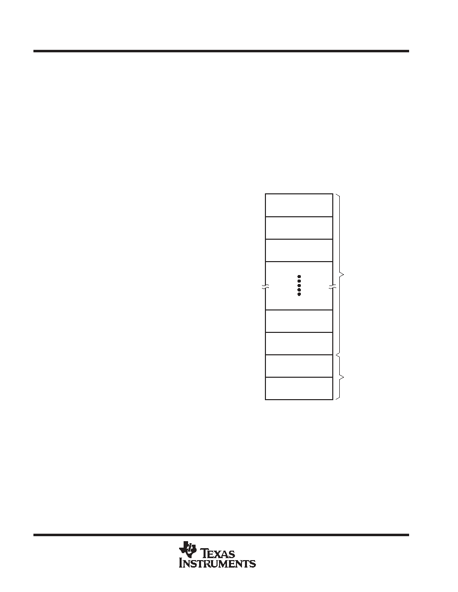
flash memory
The flash memory can be programmed via the JTAG port, the bootstrap loader, or in-system by the CPU. The
CPU can perform single-byte and single-word writes to the flash memory. Features of the flash memory include:
D
Flash memory has n segments of main memory and two segments of information memory (A and B) of 128
bytes each. Each segment in main memory is 512 bytes in size.
D
Segments 0 to n may be erased in one step, or each segment may be individually erased.
D
Segments A and B can be erased individually, or as a group with segments 0-n.
Segments A and B are also called information memory.
D
New devices may have some bytes programmed in the information memory (needed for test during
manufacturing). The user should perform an erase of the information memory prior to the first use.
Segment 0
w/ Interrupt Vectors
Segment 1
Segment 2
Segment n-1
Segment n
Segment A
Segment B
Main
Memory
Information
Memory
8 KB
0FFFFh
0FE00h
0FDFFh
0FC00h
0FBFFh
0FA00h
0F9FFh
16 KB
0FFFFh
0FE00h
0FDFFh
0FC00h
0FBFFh
0FA00h
0F9FFh
32 KB
0FFFFh
0FE00h
0FDFFh
0FC00h
0FBFFh
0FA00h
0F9FFh
48 KB
0FFFFh
0FE00h
0FDFFh
0FC00h
0FBFFh
0FA00h
0F9FFh
60 KB
0FFFFh
0FE00h
0FDFFh
0FC00h
0FBFFh
0FA00h
0F9FFh
0E400h
0E3FFh
0E200h
0E1FFh
0E000h
010FFh
01080h
0107Fh
01000h
0C400h
0C3FFh
0C200h
0C1FFh
0C000h
010FFh
01080h
0107Fh
01000h
08400h
083FFh
08200h
081FFh
08000h
010FFh
01080h
0107Fh
01000h
04400h
043FFh
04200h
041FFh
04000h
010FFh
01080h
0107Fh
01000h
01400h
013FFh
01200h
011FFh
01100h
010FFh
01080h
0107Fh
01000h

MSP430x13x, MSP430x14x, MSP430x14x1
MIXED SIGNAL MICROCONTROLLER
SLAS272F - JULY 2000 - REVISED JUNE 2004
17
POST OFFICE BOX 655303
∑
DALLAS, TEXAS 75265
peripherals
Peripherals are connected to the CPU through data, address, and control busses and can be handled using
all instructions. For complete module descriptions, see the MSP430x1xx Family User's Guide, literature number
SLAU049.
digital I/O
There are six 8-bit I/O ports implemented--ports P1 through P6:
D
All individual I/O bits are independently programmable.
D
Any combination of input, output, and interrupt conditions is possible.
D
Edge-selectable interrupt input capability for all the eight bits of ports P1 and P2.
D
Read/write access to port-control registers is supported by all instructions.
oscillator and system clock
The clock system in the MSP430x13x and MSP43x14x(1) family of devices is supported by the basic clock
module that includes support for a 32768-Hz watch crystal oscillator, an internal digitally-controlled oscillator
(DCO) and a high frequency crystal oscillator. The basic clock module is designed to meet the requirements
of both low system cost and low-power consumption. The internal DCO provides a fast turn-on clock source
and stabilizes in less than 6
µ
s. The basic clock module provides the following clock signals:
D
Auxiliary clock (ACLK), sourced from a 32768-Hz watch crystal or a high frequency crystal.
D
Main clock (MCLK), the system clock used by the CPU.
D
Sub-Main clock (SMCLK), the sub-system clock used by the peripheral modules.
watchdog timer
The primary function of the watchdog timer (WDT) module is to perform a controlled system restart after a
software problem occurs. If the selected time interval expires, a system reset is generated. If the watchdog
function is not needed in an application, the module can be configured as an interval timer and can generate
interrupts at selected time intervals.
hardware multiplier (MSP430x14x and MSP430x14x1 Only)
The multiplication operation is supported by a dedicated peripheral module. The module performs 16
16,
16
8, 8
16, and 8
8 bit operations. The module is capable of supporting signed and unsigned multiplication
as well as signed and unsigned multiply and accumulate operations. The result of an operation can be accessed
immediately after the operands have been loaded into the peripheral registers. No additional clock cycles are
required.
USART0
The MSP430x13x and the MSP430x14x(1) have one hardware universal synchronous/asynchronous receive
transmit (USART0) peripheral module that is used for serial data communication. The USART supports
synchronous SPI (3 or 4 pin) and asynchronous UART communication protocols, using double-buffered
transmit and receive channels.
USART1 (MSP430x14x and MSP430x14x1 Only)
The MSP430x14x(1) has a second hardware universal synchronous/asynchronous receive transmit (USART1)
peripheral module that is used for serial data communication. The USART supports synchronous SPI (3 or 4
pin) and asynchronous UART communication protocols, using double-buffered transmit and receive channels.
Operation of USART1 is identical to USART0.
MSP430x13x, MSP430x14x, MSP430x14x1
MIXED SIGNAL MICROCONTROLLER
SLAS272F - JULY 2000 - REVISED JUNE 2004
18
POST OFFICE BOX 655303
∑
DALLAS, TEXAS 75265
comparator_A
The primary function of the comparator_A module is to support precision slope analog-to-digital conversions,
battery-voltage supervision, and monitoring of external analog signals.
ADC12 (Not implemented in the MSP430x14x1)
The ADC12 module supports fast, 12-bit analog-to-digital conversions. The module implements a 12-bit SAR
core, sample select control, reference generator and a 16 word conversion-and-control buffer. The
conversion-and-control buffer allows up to 16 independent ADC samples to be converted and stored without
any CPU intervention.
timer_A3
Timer_A3 is a 16-bit timer/counter with three capture/compare registers. Timer_A3 can support multiple
capture/compares, PWM outputs, and interval timing. Timer_A3 also has extensive interrupt capabilities.
Interrupts may be generated from the counter on overflow conditions and from each of the capture/compare
registers.
Timer_A3 Signal Connections
Input Pin Number
Device Input Signal
Module Input Name
Module Block
Module Output Signal
Output Pin Number
12 - P1.0
TACLK
TACLK
ACLK
ACLK
Timer
NA
SMCLK
SMCLK
Timer
NA
21 - P2.1
TAINCLK
INCLK
13 - P1.1
TA0
CCI0A
13 - P1.1
22 - P2.2
TA0
CCI0B
CCR0
TA0
17 - P1.5
DVSS
GND
CCR0
TA0
27 - P2.7
DVCC
VCC
14 - P1.2
TA1
CCI1A
14 - P1.2
CAOUT (internal)
CCI1B
CCR1
TA1
18 - P1.6
DVSS
GND
CCR1
TA1
23 - P2.3
DVCC
VCC
ADC12 (internal)
15 - P1.3
TA2
CCI2A
15 - P1.3
ACLK (internal)
CCI2B
CCR2
TA2
19 - P1.7
DVSS
GND
CCR2
TA2
24 - P2.4
DVCC
VCC
timer_B3 (MSP430x13x Only)
Timer_B3 is a 16-bit timer/counter with three capture/compare registers. Timer_B3 can support multiple
capture/compares, PWM outputs, and interval timing. Timer_B3 also has extensive interrupt capabilities.
Interrupts may be generated from the counter on overflow conditions and from each of the capture/compare
registers.
MSP430x13x, MSP430x14x, MSP430x14x1
MIXED SIGNAL MICROCONTROLLER
SLAS272F - JULY 2000 - REVISED JUNE 2004
19
POST OFFICE BOX 655303
∑
DALLAS, TEXAS 75265
timer_B7 (MSP430x14x and MSP430x14x1 Only)
Timer_B7 is a 16-bit timer/counter with seven capture/compare registers. Timer_B7 can support multiple
capture/compares, PWM outputs, and interval timing. Timer_B7 also has extensive interrupt capabilities.
Interrupts may be generated from the counter on overflow conditions and from each of the capture/compare
registers.
Timer_B3/B7 Signal Connections
Input Pin Number
Device Input Signal
Module Input Name
Module Block
Module Output Signal
Output Pin Number
43 - P4.7
TBCLK
TBCLK
ACLK
ACLK
Timer
NA
SMCLK
SMCLK
Timer
NA
43 - P4.7
TBCLK
INCLK
36 - P4.0
TB0
CCI0A
36 - P4.0
36 - P4.0
TB0
CCI0B
CCR0
TB0
ADC12 (internal)
DVSS
GND
CCR0
TB0
DVCC
VCC
37 - P4.1
TB1
CCI1A
37 - P4.1
37 - P4.1
TB1
CCI1B
CCR1
TB1
ADC12 (internal)
DVSS
GND
CCR1
TB1
DVCC
VCC
38 - P4.2
TB2
CCI2A
38 - P4.2
38 - P4.2
TB2
CCI2B
CCR2
TB2
DVSS
GND
CCR2
TB2
DVCC
VCC
39 - P4.3
TB3
CCI3A
39 - P4.3
39 - P4.3
TB3
CCI3B
CCR3
TB3
DVSS
GND
CCR3
TB3
DVCC
VCC
40 - P4.4
TB4
CCI4A
40 - P4.4
40 - P4.4
TB4
CCI4B
CCR4
TB4
DVSS
GND
CCR4
TB4
DVCC
VCC
41 - P4.5
TB5
CCI5A
41 - P4.5
41 - P4.5
TB5
CCI5B
CCR5
TB5
DVSS
GND
CCR5
TB5
DVCC
VCC
42 - P4.6
TB6
CCI6A
42 - P4.6
ACLK (internal)
CCI6B
CCR6
TB6
DVSS
GND
CCR6
TB6
DVCC
VCC
Timer_B3 implements three capture/compare blocks (CCR0, CCR1 and CCR2 only).
MSP430x13x, MSP430x14x, MSP430x14x1
MIXED SIGNAL MICROCONTROLLER
SLAS272F - JULY 2000 - REVISED JUNE 2004
20
POST OFFICE BOX 655303
∑
DALLAS, TEXAS 75265
peripheral file map
PERIPHERALS WITH WORD ACCESS
Watchdog
Watchdog Timer control
WDTCTL
0120h
Timer_B7/
Timer_B3
Timer_B interrupt vector
TBIV
011Eh
Timer_B7/
Timer_B3
(see Note 1)
Timer_B control
TBCTL
0180h
(see Note 1)
Capture/compare control 0
TBCCTL0
0182h
Capture/compare control 1
TBCCTL1
0184h
Capture/compare control 2
TBCCTL2
0186h
Capture/compare control 3
TBCCTL3
0188h
Capture/compare control 4
TBCCTL4
018Ah
Capture/compare control 5
TBCCTL5
018Ch
Capture/compare control 6
TBCCTL6
018Eh
Timer_B register
TBR
0190h
Capture/compare register 0
TBCCR0
0192h
Capture/compare register 1
TBCCR1
0194h
Capture/compare register 2
TBCCR2
0196h
Capture/compare register 3
TBCCR3
0198h
Capture/compare register 4
TBCCR4
019Ah
Capture/compare register 5
TBCCR5
019Ch
Capture/compare register 6
TBCCR6
019Eh
Timer_A3
Timer_A interrupt vector
TAIV
012Eh
Timer_A3
Timer_A control
TACTL
0160h
Capture/compare control 0
TACCTL0
0162h
Capture/compare control 1
TACCTL1
0164h
Capture/compare control 2
TACCTL2
0166h
Reserved
0168h
Reserved
016Ah
Reserved
016Ch
Reserved
016Eh
Timer_A register
TAR
0170h
Capture/compare register 0
TACCR0
0172h
Capture/compare register 1
TACCR1
0174h
Capture/compare register 2
TACCR2
0176h
Reserved
0178h
Reserved
017Ah
Reserved
017Ch
Reserved
017Eh
Hardware
Multiplier
Sum extend
SUMEXT
013Eh
Hardware
Multiplier
(MSP430x14x and
Result high word
RESHI
013Ch
(MSP430x14x and
MSP430x14x1
Result low word
RESLO
013Ah
MSP430x14x1
only)
Second operand
OP2
0138h
only)
Multiply signed +accumulate/operand1
MACS
0136h
Multiply+accumulate/operand1
MAC
0134h
Multiply signed/operand1
MPYS
0132h
Multiply unsigned/operand1
MPY
0130h
NOTE 1: Timer_B7 in MSP430x14x(1) family has 7 CCRs, Timer_B3 in MSP430x13x family has 3 CCRs.
MSP430x13x, MSP430x14x, MSP430x14x1
MIXED SIGNAL MICROCONTROLLER
SLAS272F - JULY 2000 - REVISED JUNE 2004
21
POST OFFICE BOX 655303
∑
DALLAS, TEXAS 75265
peripheral file map (continued)
PERIPHERALS WITH WORD ACCESS (CONTINUED)
Flash
Flash control 3
FCTL3
012Ch
Flash
Flash control 2
FCTL2
012Ah
Flash control 1
FCTL1
0128h
ADC12
(Not implemented in
Conversion memory 15
ADC12MEM15
015Eh
ADC12
(Not implemented in
the MSP430x14x1)
Conversion memory 14
ADC12MEM14
015Ch
the MSP430x14x1)
Conversion memory 13
ADC12MEM13
015Ah
Conversion memory 12
ADC12MEM12
0158h
Conversion memory 11
ADC12MEM11
0156h
Conversion memory 10
ADC12MEM10
0154h
Conversion memory 9
ADC12MEM9
0152h
Conversion memory 8
ADC12MEM8
0150h
Conversion memory 7
ADC12MEM7
014Eh
Conversion memory 6
ADC12MEM6
014Ch
Conversion memory 5
ADC12MEM5
014Ah
Conversion memory 4
ADC12MEM4
0148h
Conversion memory 3
ADC12MEM3
0146h
Conversion memory 2
ADC12MEM2
0144h
Conversion memory 1
ADC12MEM1
0142h
Conversion memory 0
ADC12MEM0
0140h
Interrupt-vector-word register
ADC12IV
01A8h
Inerrupt-enable register
ADC12IE
01A6h
Inerrupt-flag register
ADC12IFG
01A4h
Control register 1
ADC12CTL1
01A2h
Control register 0
ADC12CTL0
01A0h
ADC memory-control register15
ADC12MCTL15
08Fh
ADC memory-control register14
ADC12MCTL14
08Eh
ADC memory-control register13
ADC12MCTL13
08Dh
ADC memory-control register12
ADC12MCTL12
08Ch
ADC memory-control register11
ADC12MCTL11
08Bh
ADC memory-control register10
ADC12MCTL10
08Ah
ADC memory-control register9
ADC12MCTL9
089h
ADC memory-control register8
ADC12MCTL8
088h
ADC memory-control register7
ADC12MCTL7
087h
ADC memory-control register6
ADC12MCTL6
086h
ADC memory-control register5
ADC12MCTL5
085h
ADC memory-control register4
ADC12MCTL4
084h
ADC memory-control register3
ADC12MCTL3
083h
ADC memory-control register2
ADC12MCTL2
082h
ADC memory-control register1
ADC12MCTL1
081h
ADC memory-control register0
ADC12MCTL0
080h
MSP430x13x, MSP430x14x, MSP430x14x1
MIXED SIGNAL MICROCONTROLLER
SLAS272F - JULY 2000 - REVISED JUNE 2004
22
POST OFFICE BOX 655303
∑
DALLAS, TEXAS 75265
peripheral file map (continued)
PERIPHERALS WITH BYTE ACCESS
USART1
(MSP430x14x and
Transmit buffer
U1TXBUF
07Fh
USART1
(MSP430x14x and
MSP430x14x1 only)
Receive buffer
U1RXBUF
07Eh
MSP430x14x1 only)
Baud rate
U1BR1
07Dh
Baud rate
U1BR0
07Ch
Modulation control
U1MCTL
07Bh
Receive control
U1RCTL
07Ah
Transmit control
U1TCTL
079h
USART control
U1CTL
078h
USART0
Transmit buffer
U0TXBUF
077h
USART0
Receive buffer
U0RXBUF
076h
Baud rate
U0BR1
075h
Baud rate
U0BR0
074h
Modulation control
U0MCTL
073h
Receive control
U0RCTL
072h
Transmit control
U0TCTL
071h
USART control
U0CTL
070h
Comparator_A
Comparator_A port disable
CAPD
05Bh
Comparator_A
Comparator_A control2
CACTL2
05Ah
Comparator_A control1
CACTL1
059h
Basic Clock
Basic clock system control2
BCSCTL2
058h
Basic Clock
Basic clock system control1
BCSCTL1
057h
DCO clock frequency control
DCOCTL
056h
Port P6
Port P6 selection
P6SEL
037h
Port P6
Port P6 direction
P6DIR
036h
Port P6 output
P6OUT
035h
Port P6 input
P6IN
034h
Port P5
Port P5 selection
P5SEL
033h
Port P5
Port P5 direction
P5DIR
032h
Port P5 output
P5OUT
031h
Port P5 input
P5IN
030h
Port P4
Port P4 selection
P4SEL
01Fh
Port P4
Port P4 direction
P4DIR
01Eh
Port P4 output
P4OUT
01Dh
Port P4 input
P4IN
01Ch
Port P3
Port P3 selection
P3SEL
01Bh
Port P3
Port P3 direction
P3DIR
01Ah
Port P3 output
P3OUT
019h
Port P3 input
P3IN
018h
Port P2
Port P2 selection
P2SEL
02Eh
Port P2
Port P2 interrupt enable
P2IE
02Dh
Port P2 interrupt-edge select
P2IES
02Ch
Port P2 interrupt flag
P2IFG
02Bh
Port P2 direction
P2DIR
02Ah
Port P2 output
P2OUT
029h
Port P2 input
P2IN
028h
MSP430x13x, MSP430x14x, MSP430x14x1
MIXED SIGNAL MICROCONTROLLER
SLAS272F - JULY 2000 - REVISED JUNE 2004
23
POST OFFICE BOX 655303
∑
DALLAS, TEXAS 75265
peripheral file map (continued)
PERIPHERALS WITH BYTE ACCESS (CONTINUED)
Port P1
Port P1 selection
P1SEL
026h
Port P1
Port P1 interrupt enable
P1IE
025h
Port P1 interrupt-edge select
P1IES
024h
Port P1 interrupt flag
P1IFG
023h
Port P1 direction
P1DIR
022h
Port P1 output
P1OUT
021h
Port P1 input
P1IN
020h
Special Functions
SFR module enable 2
ME2
005h
Special Functions
SFR module enable 1
ME1
004h
SFR interrupt flag2
IFG2
003h
SFR interrupt flag1
IFG1
002h
SFR interrupt enable2
IE2
001h
SFR interrupt enable1
IE1
000h
absolute maximum ratings over operating free-air temperature (unless otherwise noted)
Voltage applied at V
CC
to V
SS
-0.3 V to + 4.1 V
. . . . . . . . . . . . . . . . . . . . . . . . . . . . . . . . . . . . . . . . . . . . . . . . . . . .
Voltage applied to any pin (see Note)
-0.3 V to V
CC
+0.3 V
. . . . . . . . . . . . . . . . . . . . . . . . . . . . . . . . . . . . . . . . . . .
Diode current at any device terminal .
±
2 mA
. . . . . . . . . . . . . . . . . . . . . . . . . . . . . . . . . . . . . . . . . . . . . . . . . . . . . .
Storage temperature (unprogrammed device)
-55
∞
C to 150
∞
C
. . . . . . . . . . . . . . . . . . . . . . . . . . . . . . . . . . . . . . .
Storage temperature (programmed device)
-40
∞
C to 85
∞
C
. . . . . . . . . . . . . . . . . . . . . . . . . . . . . . . . . . . . . . . . . .
Stresses beyond those listed under "absolute maximum ratings" may cause permanent damage to the device. These are stress ratings only, and
functional operation of the device at these or any other conditions beyond those indicated under "recommended operating conditions" is not
implied. Exposure to absolute-maximum-rated conditions for extended periods may affect device reliability.
NOTE: All voltages referenced to VSS. The JTAG fuse-blow voltage, VFB, is allowed to exceed the absolute maximum rating. The voltage is applied
to the TDI/TCLK pin when blowing the JTAG fuse.
MSP430x13x, MSP430x14x, MSP430x14x1
MIXED SIGNAL MICROCONTROLLER
SLAS272F - JULY 2000 - REVISED JUNE 2004
24
POST OFFICE BOX 655303
∑
DALLAS, TEXAS 75265
recommended operating conditions
PARAMETER
MIN
NOM
MAX
UNITS
Supply voltage during program execution, VCC (AVCC = DVCC = VCC)
MSP430F13x,
MSP430F14x(1)
1.8
3.6
V
Supply voltage during flash memory programming, VCC
(AVCC = DVCC = VCC)
MSP430F13x,
MSP430F14x(1)
2.7
3.6
V
Supply voltage, VSS (AVSS = DVSS = VSS)
0.0
0.0
V
Operating free-air temperature range, TA
MSP430x13x
MSP430x14x(1)
-40
85
∞
C
LFXT1 crystal frequency, f(LFXT1)
LF selected, XTS=0
Watch crystal
32768
Hz
LFXT1 crystal frequency, f(LFXT1)
(see Notes 1 and 2)
XT1 selected, XTS=1
Ceramic resonator
450
8000
kHz
(see Notes 1 and 2)
XT1 selected, XTS=1
Crystal
1000
8000
kHz
XT2 crystal frequency, f(XT2)
Ceramic resonator
450
8000
kHz
XT2 crystal frequency, f(XT2)
Crystal
1000
8000
kHz
Processor frequency (signal MCLK), f(System)
VCC = 1.8 V
DC
4.15
MHz
Processor frequency (signal MCLK), f(System)
VCC = 3.6 V
DC
8
MHz
NOTES:
1. In LF mode, the LFXT1 oscillator requires a watch crystal. A 5.1M
resistor from XOUT to VSS is recommended when VCC <
2.5 V. In XT1 mode, the LFXT1 and XT2 oscillators accept a ceramic resonator or crystal up to 4.15MHz at VCC
2.2 V. In XT1 mode,
the LFXT1 and XT2 oscillators accept a ceramic resonator or crystal up to 8MHz at VCC
2.8 V.
2. In LF mode, the LFXT1 oscillator requires a watch crystal. In XT1 mode, LFXT1 accepts a ceramic resonator or a crystal.
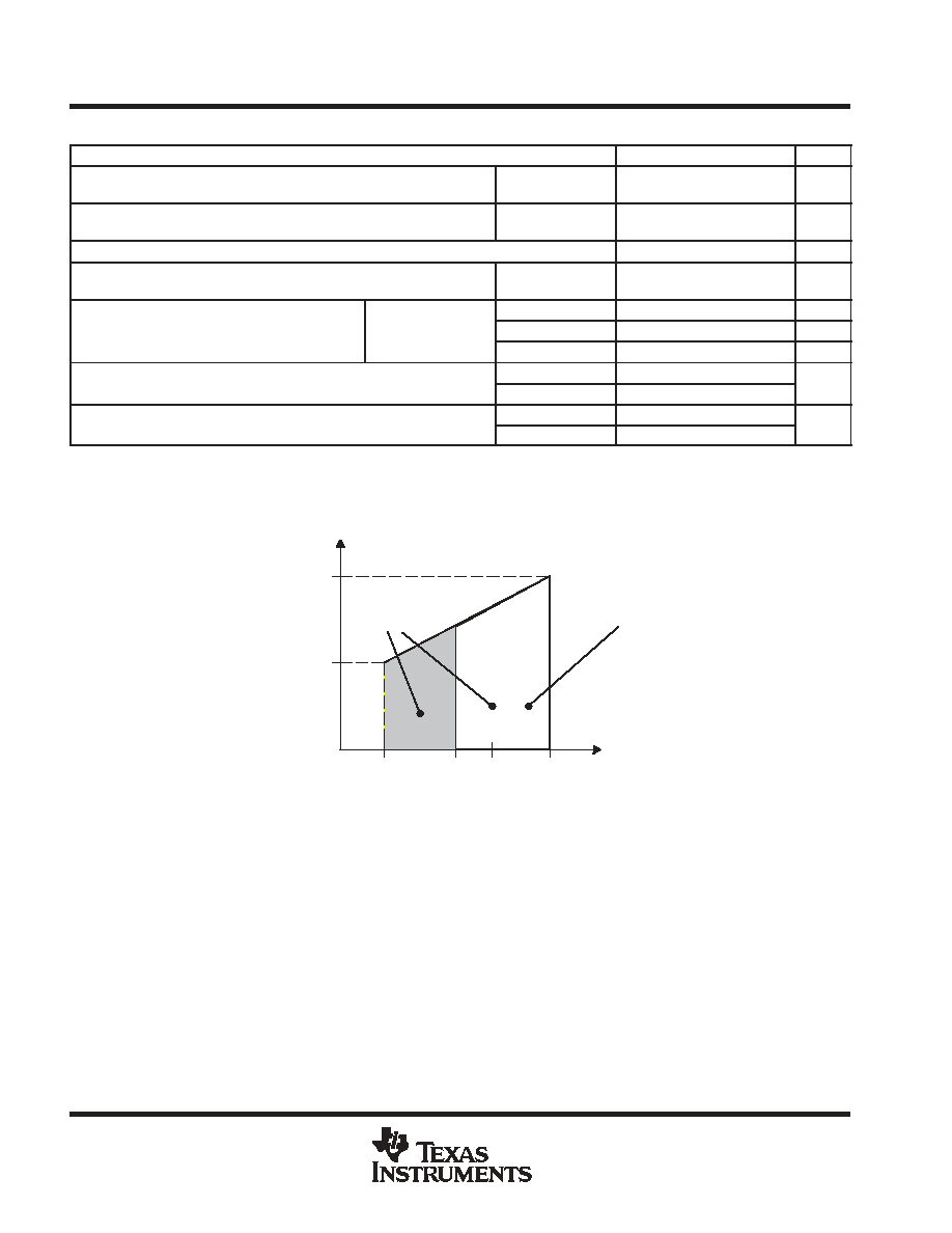
f (MHz)
1.8 V
3.6 V
2.7 V 3 V
ŒŒŒŒŒ
ŒŒŒŒŒ
ŒŒŒŒŒ
ŒŒŒŒŒ
ŒŒŒŒŒ
ŒŒŒŒŒ
ŒŒŒŒŒ
ŒŒŒŒŒ
4.15 MHz
8.0 MHz
Supply Voltage - V
Supply voltage range, 'F13x/'F14x(1),
during flash memory programming
Supply voltage range,
'F13x/'F14x(1), during
program execution
Figure 1. Frequency vs Supply Voltage, MSP430F13x or MSP430F14x(1)
MSP430x13x, MSP430x14x, MSP430x14x1
MIXED SIGNAL MICROCONTROLLER
SLAS272F - JULY 2000 - REVISED JUNE 2004
25
POST OFFICE BOX 655303
∑
DALLAS, TEXAS 75265
electrical characteristics over recommended operating free-air temperature (unless otherwise
noted)
supply current into AV
CC
+ DV
CC
excluding external current
PARAMETER
TEST CONDITIONS
MIN
NOM
MAX
UNIT
I(AM)
Active mode, (see Note 1)
f(MCLK) = f(SMCLK) = 1 MHz,
TA = -40
∞
C to 85
∞
C
VCC = 2.2 V
280
350
A
I(AM)
f(MCLK) = f(SMCLK) = 1 MHz,
f(ACLK) = 32,768 Hz
XTS=0, SELM=(0,1)
TA = -40
∞
C to 85
∞
C
VCC = 3 V
420
560
µ
A
I(AM)
Active mode, (see Note 1)
f(MCLK) = f(SMCLK) = 4 096 Hz,
f(ACLK) = 4,096 Hz
TA = -40
∞
C to 85
∞
C
VCC = 2.2 V
2.5
7
A
I(AM)
(MCLK)
(SMCLK)
f(ACLK) = 4,096 Hz
XTS=0, SELM=(0,1)
XTS=0, SELM=3
TA = -40
∞
C to 85
∞
C
VCC = 3 V
9
20
µ
A
I(LPM0)
Low-power mode, (LPM0)
TA = -40
∞
C to 85
∞
C
VCC = 2.2 V
32
45
A
I(LPM0)
Low-power mode, (LPM0)
(see Note 1)
TA = -40
∞
C to 85
∞
C
VCC = 3 V
55
70
µ
A
I(LPM2)
Low-power mode, (LPM2),
f(MCLK) = f (SMCLK) = 0 MHz,
TA = -40
∞
C to 85
∞
C
VCC = 2.2 V
11
14
A
I(LPM2)
f(MCLK) = f (SMCLK) = 0 MHz,
f(ACLK) = 32.768 Hz, SCG0 = 0
TA = -40
∞
C to 85
∞
C
VCC = 3 V
17
22
µ
A
TA = -40
∞
C
0.8
1.5
Low-power mode, (LPM3)
TA = 25
∞
C
VCC = 2.2 V
0.9
1.5
µ
A
I(LPM3)
Low-power mode, (LPM3)
f(MCLK) = f(SMCLK) = 0 MHz,
TA = 85
∞
C
VCC = 2.2 V
1.6
2.8
µ
A
I(LPM3)
f(MCLK) = f(SMCLK) = 0 MHz,
f(ACLK) = 32,768 Hz, SCG0 = 1 (see Note 2)
TA = -40
∞
C
1.8
2.2
f(ACLK) = 32,768 Hz, SCG0 = 1 (see Note 2)
TA = 25
∞
C
VCC = 3 V
1.6
1.9
µ
A
TA = 85
∞
C
VCC = 3 V
2.3
3.9
µ
A
TA = -40
∞
C
0.1
0.5
Low-power mode, (LPM4)
TA = 25
∞
C
VCC = 2.2 V
0.1
0.5
µ
A
I(LPM4)
Low-power mode, (LPM4)
f(MCLK) = 0 MHz, f(SMCLK) = 0 MHz,
TA = 85
∞
C
VCC = 2.2 V
0.8
2.5
µ
A
I(LPM4)
f(MCLK) = 0 MHz, f(SMCLK) = 0 MHz,
f(ACLK) = 0 Hz, SCG0 = 1
TA = -40
∞
C
0.1
0.5
f(ACLK) = 0 Hz, SCG0 = 1
TA = 25
∞
C
VCC = 3 V
0.1
0.5
µ
A
TA = 85
∞
C
VCC = 3 V
0.8
2.5
µ
A
NOTES:
1. Timer_B is clocked by f(DCOCLK) = 1 MHz. All inputs are tied to 0 V or to VCC. Outputs do not source or sink any current.
2. Timer_B is clocked by f(ACLK) = 32,768 Hz. All inputs are tied to 0 V or to VCC. Outputs do not source or sink any current. The current
consumption in LPM2 and LPM3 are measured with ACLK selected.
Current consumption of active mode versus system frequency, F-version
I(AM) = I(AM) [1 MHz]
◊
f(System) [MHz]
Current consumption of active mode versus supply voltage, F-version
I
(AM)
= I
(AM) [3 V]
+ 175
µ
A/V
◊
(V
CC
≠ 3 V)
MSP430x13x, MSP430x14x, MSP430x14x1
MIXED SIGNAL MICROCONTROLLER
SLAS272F - JULY 2000 - REVISED JUNE 2004
26
POST OFFICE BOX 655303
∑
DALLAS, TEXAS 75265
electrical characteristics over recommended operating free-air temperature (unless otherwise
noted) (continued)
SCHMITT-trigger inputs - Ports P1, P2, P3, P4, P5, and P6
PARAMETER
TEST CONDITIONS
MIN
TYP
MAX
UNIT
VIT+
Positive-going input threshold voltage
VCC = 2.2 V
1.1
1.5
V
VIT+
Positive-going input threshold voltage
VCC = 3 V
1.5
1.9
V
VIT-
Negative-going input threshold voltage
VCC = 2.2 V
0.4
0.9
V
VIT-
Negative-going input threshold voltage
VCC = 3 V
0.90
1.3
V
Vhys
Input voltage hysteresis (VIT+ - VIT-)
VCC = 2.2 V
0.3
1.1
V
Vhys
Input voltage hysteresis (VIT+ - VIT-)
VCC = 3 V
0.5
1
V
standard inputs - RST/NMI; JTAG: TCK, TMS, TDI/TCLK, TDO/TDI
PARAMETER
TEST CONDITIONS
MIN
TYP
MAX
UNIT
VIL
Low-level input voltage
VCC = 2.2 V / 3 V
VSS
VSS+0.6
V
VIH
High-level input voltage
VCC = 2.2 V / 3 V
0.8
◊
VCC
VCC
V
inputs Px.x, TAx, TBx
PARAMETER
TEST CONDITIONS
VCC
MIN
TYP
MAX
UNIT
Port P1, P2: P1.x to P2.x, external trigger signal
2.2 V/3 V
1.5
cycle
t(int)
External interrupt timing
Port P1, P2: P1.x to P2.x, external trigger signal
for the interrupt flag, (see Note 1)
2.2 V
62
ns
t(int)
External interrupt timing
for the interrupt flag, (see Note 1)
3 V
50
ns
Timer_A, Timer_B capture
TA0, TA1, TA2
2.2 V
62
t(cap)
Timer_A, Timer_B capture
timing
TB0, TB1, TB2, TB3, TB4, TB5, TB6 (see
Note 2)
3 V
50
ns
f(TAext)
Timer_A, Timer_B clock
frequency externally applied
TACLK, TBCLK, INCLK: t(H) = t(L)
2.2 V
8
MHz
f(TBext)
frequency externally applied
to pin
TACLK, TBCLK, INCLK: t(H) = t(L)
3 V
10
MHz
f(TAint)
Timer_A, Timer_B clock
frequency
SMCLK or ACLK signal selected
2.2 V
8
MHz
f(TBint)
Timer_A, Timer_B clock
frequency
SMCLK or ACLK signal selected
3 V
10
MHz
NOTES:
1. The external signal sets the interrupt flag every time the minimum t(int) cycle and time parameters are met. It may be set even with
trigger signals shorter than t(int). Both the cycle and timing specifications must be met to ensure the flag is set. t(int) is measured in
MCLK cycles.
2. Seven capture/compare registers in 'x14x(1) and three capture/compare registers in 'x13x.
leakage current (see Note 1)
PARAMETER
TEST CONDITIONS
MIN
TYP
MAX
UNIT
Ilkg(P1.x)
Leakage
Port P1
V(P1.x) (see Note 2)
±
50
Ilkg(P2.x)
Leakage
current (see
Note 1)
Port P2
V(P2.3) V(P2.4) (see Note 2)
VCC = 2.2 V/3 V
±
50
nA
Ilkg(P6.x)
current (see
Note 1)
Port P6
V(P6.x) (see Note 2)
VCC = 2.2 V/3 V
±
50
nA
NOTES:
1. The leakage current is measured with VSS or VCC applied to the corresponding pin(s), unless otherwise noted.
2. The port pin must be selected as input and there must be no optional pullup or pulldown resistor.
MSP430x13x, MSP430x14x, MSP430x14x1
MIXED SIGNAL MICROCONTROLLER
SLAS272F - JULY 2000 - REVISED JUNE 2004
27
POST OFFICE BOX 655303
∑
DALLAS, TEXAS 75265
electrical characteristics over recommended operating free-air temperature (unless otherwise
noted) (continued)
outputs - Ports P1, P2, P3, P4, P5, and P6
PARAMETER
TEST CONDITIONS
MIN
TYP
MAX
UNIT
IOH(max) = -1 mA,
VCC = 2.2 V,
See Note 1
VCC-0.25
VCC
VOH
High-level output voltage
IOH(max) = -6 mA,
VCC = 2.2 V,
See Note 2
VCC-0.6
VCC
V
VOH
High-level output voltage
IOH(max) = -1 mA,
VCC = 3 V,
See Note 1
VCC-0.25
VCC
V
IOH(max) = -6 mA,
VCC = 3 V,
See Note 2
VCC-0.6
VCC
IOL(max) = 1.5 mA,
VCC = 2.2 V,
See Note 1
VSS
VSS+0.25
VOL
Low-level output voltage
IOL(max) = 6 mA,
VCC = 2.2 V,
See Note 2
VSS
VSS+0.6
V
VOL
Low-level output voltage
IOL(max) = 1.5 mA,
VCC = 3 V,
See Note 1
VSS
VSS+0.25
V
IOL(max) = 6 mA,
VCC = 3 V,
See Note 2
VSS
VSS+0.6
NOTES:
1. The maximum total current, IOH(max) and IOL(max), for all outputs combined, should not exceed
±
6 mA to satisfy the maximum
specified voltage drop.
2. The maximum total current, IOH(max) and IOL(max), for all outputs combined, should not exceed
±
24 mA to satisfy the maximum
specified voltage drop.
output frequency
PARAMETER
TEST CONDITIONS
MIN
TYP
MAX
UNIT
fTAx
TA0..2, TB0-TB6,
Internal clock source, SMCLK signal
applied (see Note 1)
CL = 20 pF
DC
fSystem
MHz
fACLK,
fMCLK,
fSMCLK
P5.6/ACLK, P5.4/MCLK, P5.5/SMCLK
CL = 20 pF
fSystem
MHz
P2.0/ACLK
fACLK = fLFXT1 = fXT1
40%
60%
P2.0/ACLK
CL = 20 pF,
V
= 2.2 V / 3 V
fACLK = fLFXT1 = fLF
30%
70%
CL = 20 pF,
VCC = 2.2 V / 3 V fACLK = fLFXT1/n
50%
fSMCLK = fLFXT1 = fXT1
40%
60%
tXdc
Duty cycle of output frequency,
P1.4/SMCLK,
fSMCLK = fLFXT1 = fLF
35%
65%
Xdc
P1.4/SMCLK,
CL = 20 pF,
VCC = 2.2 V / 3 V
fSMCLK = fLFXT1/n
50%-
15 ns
50%
50%-
15 ns
VCC = 2.2 V / 3 V
fSMCLK = fDCOCLK
50%-
15 ns
50%
50%-
15 ns
NOTE 1: The limits of the system clock MCLK has to be met; the system (MCLK) frequency should not exceed the limits. MCLK and SMCLK
frequencies can be different.
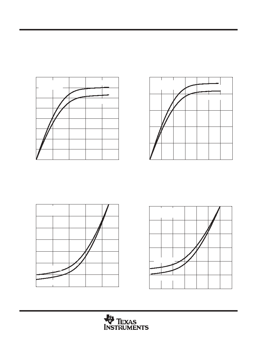
MSP430x13x, MSP430x14x, MSP430x14x1
MIXED SIGNAL MICROCONTROLLER
SLAS272F - JULY 2000 - REVISED JUNE 2004
28
POST OFFICE BOX 655303
∑
DALLAS, TEXAS 75265
electrical characteristics over recommended operating free-air temperature (unless otherwise
noted) (continued)
outputs - Ports P1, P2, P3, P4, P5, and P6 (continued)
Figure 2
VOL - Low-Level Output Voltage - V
0
2
4
6
8
10
12
14
16
0.0
0.5
1.0
1.5
2.0
2.5
VCC = 2.2 V
P2.7
TYPICAL LOW-LEVEL OUTPUT CURRENT
vs
LOW-LEVEL OUTPUT VOLTAGE
TA = 25
∞
C
TA = 85
∞
C
OLI
-
Low-Level Output Current - mA
Figure 3
VOL - Low-Level Output Voltage - V
0
5
10
15
20
25
0.0
0.5
1.0
1.5
2.0
2.5
3.0
3.5
VCC = 3 V
P2.7
TYPICAL LOW-LEVEL OUTPUT CURRENT
vs
LOW-LEVEL OUTPUT VOLTAGE
TA = 25
∞
C
TA = 85
∞
C
OLI
-
Low-Level Output Current - mA
Figure 4
VOH - High-Level Output Voltage - V
-14
-12
-10
-8
-6
-4
-2
0
0.0
0.5
1.0
1.5
2.0
2.5
VCC = 2.2 V
P2.7
TYPICAL HIGH-LEVEL OUTPUT CURRENT
vs
HIGH-LEVEL OUTPUT VOLTAGE
TA = 25
∞
C
TA = 85
∞
C
OHI
-
High-Level Output Current - mA
Figure 5
VOH - High-Level Output Voltage - V
-30
-25
-20
-15
-10
-5
0
0.0
0.5
1.0
1.5
2.0
2.5
3.0
3.5
VCC = 3 V
P2.7
TYPICAL HIGH-LEVEL OUTPUT CURRENT
vs
HIGH-LEVEL OUTPUT VOLTAGE
TA = 25
∞
C
TA = 85
∞
C
OHI
-
High-Level Output Current - mA
MSP430x13x, MSP430x14x, MSP430x14x1
MIXED SIGNAL MICROCONTROLLER
SLAS272F - JULY 2000 - REVISED JUNE 2004
29
POST OFFICE BOX 655303
∑
DALLAS, TEXAS 75265
electrical characteristics over recommended operating free-air temperature (unless otherwise
noted) (continued)
wake-up LPM3
PARAMETER
TEST CONDITIONS
MIN
TYP
MAX
UNIT
f = 1 MHz
6
t(LPM3) Delay time
f = 2 MHz
VCC = 2.2 V/3 V
6
µ
s
t(LPM3) Delay time
f = 3 MHz
VCC = 2.2 V/3 V
6
µ
s
RAM
PARAMETER
TEST CONDITIONS
MIN
TYP
MAX
UNIT
VRAMh
CPU HALTED (see Note 1)
1.6
V
NOTE 1: This parameter defines the minimum supply voltage when the data in program memory RAM remain unchanged. No program execution
should take place during this supply voltage condition.
Comparator_A (see Note 1)
PARAMETER
TEST CONDITIONS
MIN
TYP
MAX
UNIT
I(DD)
CAON=1, CARSEL=0, CAREF=0
VCC = 2.2 V
25
40
µ
A
I(DD)
CAON=1, CARSEL=0, CAREF=0
VCC = 3 V
45
60
µ
A
I(Refladder/Refdiode)
CAON=1, CARSEL=0,
CAREF=1/2/3, no load at
VCC = 2.2 V
30
50
µ
A
I(Refladder/Refdiode)
CAREF=1/2/3, no load at
P2.3/CA0/TA1 and P2.4/CA1/TA2
VCC = 3 V
45
71
µ
A
V(IC)
Common-mode input
voltage
CAON =1
VCC = 2.2 V/3 V
0
VCC-1
V
V(Ref025)
Voltage @ 0.25 V
CC
node
V
CC
PCA0=1, CARSEL=1, CAREF=1,
no load at P2.3/CA0/TA1 and
P2.4/CA1/TA2
VCC = 2.2 V/3 V
0.23
0.24
0.25
V(Ref050)
Voltage @ 0.5V
CC
node
V
CC
PCA0=1, CARSEL=1, CAREF=2,
no load at P2.3/CA0/TA1 and
P2.4/CA1/TA2
VCC = 2.2 V/3 V
0.47
0.48
0.5
V(RefVT)
(see Figure 6)
PCA0=1, CARSEL=1, CAREF=3,
no load at P2.3/CA0/TA1 and
VCC = 2.2 V
390
480
540
mV
V(RefVT)
(see Figure 6)
no load at P2.3/CA0/TA1 and
P2.4/CA1/TA2 TA = 85
∞
C
VCC = 3 V
400
490
550
mV
V(offset)
Offset voltage
See Note 2
VCC = 2.2 V/3 V
-30
30
mV
Vhys
Input hysteresis
CAON=1
VCC = 2.2 V/3 V
0
0.7
1.4
mV
TA = 25
∞
C, Overdrive 10 mV,
VCC = 2.2 V
130
210
300
ns
t(response LH)
TA = 25 C, Overdrive 10 mV,
Without filter: CAF=0
VCC = 3 V
80
150
240
ns
t(response LH)
TA = 25
∞
C, Overdrive 10 mV,
VCC = 2.2 V
1.4
1.9
3.4
µ
s
TA = 25 C, Overdrive 10 mV,
With filter: CAF=1
VCC = 3 V
0.9
1.5
2.6
µ
s
TA = 25
∞
C, Overdrive 10 mV,
VCC = 2.2 V
130
210
300
ns
t(response HL)
TA = 25 C, Overdrive 10 mV,
Without filter: CAF=0
VCC = 3 V
80
150
240
ns
t(response HL)
TA = 25
∞
C, Overdrive 10 mV,
VCC = 2.2 V
1.4
1.9
3.4
µ
s
TA = 25 C, Overdrive 10 mV,
With filter: CAF=1
VCC = 3 V
0.9
1.5
2.6
µ
s
NOTES:
1. The leakage current for the Comparator_A terminals is identical to Ilkg(Px.x) specification.
2. The input offset voltage can be cancelled by using the CAEX bit to invert the Comparator_A inputs on successive measurements.
The two successive measurements are then summed together.
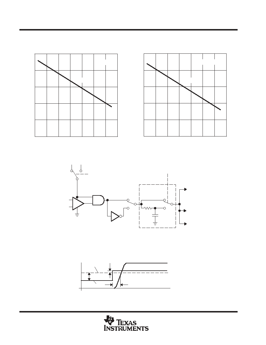
MSP430x13x, MSP430x14x, MSP430x14x1
MIXED SIGNAL MICROCONTROLLER
SLAS272F - JULY 2000 - REVISED JUNE 2004
30
POST OFFICE BOX 655303
∑
DALLAS, TEXAS 75265
electrical characteristics over recommended operating free-air temperature (unless otherwise
noted) (continued)
TA - Free-Air Temperature -
∞
C
400
450
500
550
600
650
-45
-25
-5
15
35
55
75
95
VCC = 3 V
Figure 6. V
(RefVT)
vs Temperature, V
CC
= 3 V
V
(REFVT)
- Reference V
olts -mV
Typical
Figure 7. V
(RefVT)
vs Temperature, V
CC
= 2.2 V
TA - Free-Air Temperature -
∞
C
400
450
500
550
600
650
-45
-25
-5
15
35
55
75
95
VCC = 2.2 V
V
(REFVT)
- Reference V
olts -mV
Typical
_
+
CAON
0
1
V+
0
1
CAF
Low Pass Filter
2.0
µ
s
To Internal
Modules
Set CAIFG
Flag
CAOUT
V-
VCC
1
0 V
0
Figure 8. Block Diagram of Comparator_A Module
Overdrive
VCAOUT
t(response)
V+
V-
400 mV
Figure 9. Overdrive Definition
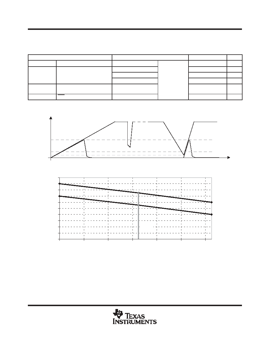
MSP430x13x, MSP430x14x, MSP430x14x1
MIXED SIGNAL MICROCONTROLLER
SLAS272F - JULY 2000 - REVISED JUNE 2004
31
POST OFFICE BOX 655303
∑
DALLAS, TEXAS 75265
electrical characteristics over recommended operating free-air temperature (unless otherwise
noted) (continued)
PUC/POR
PARAMETER
TEST CONDITIONS
MIN
TYP
MAX
UNIT
t(POR_Delay)
Internal time delay to release POR
150
250
µ
s
VCC threshold at which POR
TA = -40
∞
C
1.4
1.8
V
VPOR
VCC threshold at which POR
release delay time begins
(see Note 1)
TA = 25
∞
C
1.1
1.5
V
VPOR
release delay time begins
(see Note 1)
TA = 85
∞
C
VCC = 2.2 V/3 V
0.8
1.2
V
V(min)
VCC threshold required to
generate a POR (see Note 2)
VCC |dV/dt|
1V/ms
CC
0.2
V
t(reset)
RST/NMI low time for PUC/POR
Reset is accepted internally
2
µ
s
NOTES:
1. VCC rise time dV/dt
1V/ms.
2. When driving VCC low in order to generate a POR condition, VCC should be driven to 200mV or lower with a dV/dt equal to or less
than -1V/ms. The corresponding rising VCC must also meet the dV/dt requirement equal to or greater than +1V/ms.
VCC
POR
V
t
V
POR
V
(min)
POR
No POR
Figure 10. Power-On Reset (POR) vs Supply Voltage
1.2
1.5
1.8
0.8
1.2
1.4
0
0.2
0.4
0.6
0.8
1
1.2
1.4
1.6
1.8
2
-40
-20
0
20
40
60
80
25
∞
C
TA - Temperature -
∞
C
V
POR
- V
Figure 11. V
POR
vs Temperature
MSP430x13x, MSP430x14x, MSP430x14x1
MIXED SIGNAL MICROCONTROLLER
SLAS272F - JULY 2000 - REVISED JUNE 2004
32
POST OFFICE BOX 655303
∑
DALLAS, TEXAS 75265
electrical characteristics over recommended operating free-air temperature (unless otherwise
noted) (continued)
DCO (see Note 1)
PARAMETER
TEST CONDITIONS
MIN
NOM
MAX
UNIT
f(DCO03)
Rsel = 0, DCO = 3, MOD = 0, DCOR = 0, TA = 25
∞
C
VCC = 2.2 V
0.08
0.12
0.15
MHz
f(DCO03)
VCC = 3 V
0.08
0.13
0.16
MHz
f(DCO13)
Rsel = 1, DCO = 3, MOD = 0, DCOR = 0, TA = 25
∞
C
VCC = 2.2 V
0.14
0.19
0.23
MHz
f(DCO13)
VCC = 3 V
0.14
0.18
0.22
MHz
f(DCO23)
Rsel = 2, DCO = 3, MOD = 0, DCOR = 0, TA = 25
∞
C
VCC = 2.2 V
0.22
0.30
0.36
MHz
f(DCO23)
VCC = 3 V
0.22
0.28
0.34
MHz
f(DCO33)
Rsel = 3, DCO = 3, MOD = 0, DCOR = 0, TA = 25
∞
C
VCC = 2.2 V
0.37
0.49
0.59
MHz
f(DCO33)
VCC = 3 V
0.37
0.47
0.56
MHz
f(DCO43)
Rsel = 4, DCO = 3, MOD = 0, DCOR = 0, TA = 25
∞
C
VCC = 2.2 V
0.61
0.77
0.93
MHz
f(DCO43)
VCC = 3 V
0.61
0.75
0.90
MHz
f(DCO53)
Rsel = 5, DCO = 3, MOD = 0, DCOR = 0, TA = 25
∞
C
VCC = 2.2 V
1
1.2
1.5
MHz
f(DCO53)
VCC = 3 V
1
1.3
1.5
MHz
f(DCO63)
Rsel = 6, DCO = 3, MOD = 0, DCOR = 0, TA = 25
∞
C
VCC = 2.2 V
1.6
1.9
2.2
MHz
f(DCO63)
VCC = 3 V
1.69
2.0
2.29
MHz
f(DCO73)
Rsel = 7, DCO = 3, MOD = 0, DCOR = 0, TA = 25
∞
C
VCC = 2.2 V
2.4
2.9
3.4
MHz
f(DCO73)
VCC = 3 V
2.7
3.2
3.65
MHz
f(DCO47)
Rsel = 4, DCO = 7, MOD = 0, DCOR = 0, TA = 25
∞
C
VCC = 2.2 V/3 V
fDCO40
◊
1.7
fDCO40
◊
2.1
fDCO40
◊
2.5
MHz
f(DCO77)
Rsel = 7, DCO = 7, MOD = 0, DCOR = 0, TA = 25
∞
C
VCC = 2.2 V
4
4.5
4.9
MHz
f(DCO77)
Rsel = 7, DCO = 7, MOD = 0, DCOR = 0, TA = 25
∞
C
VCC = 3 V
4.4
4.9
5.4
MHz
S(Rsel)
SR = fRsel+1 / fRsel
VCC = 2.2 V/3 V
1.35
1.65
2
S(DCO)
SDCO = fDCO+1 / fDCO
VCC = 2.2 V/3 V
1.07
1.12
1.16
Dt
Temperature drift, Rsel = 4, DCO = 3, MOD = 0
VCC = 2.2 V
-0.31
-0.36
-0.40
%/
∞
C
Dt
Temperature drift, Rsel = 4, DCO = 3, MOD = 0
(see Note 2)
VCC = 3 V
-0.33
-0.38
-0.43
%/
∞
C
DV
Drift with VCC variation, Rsel = 4, DCO = 3, MOD = 0
(see Note 2)
VCC = 2.2 V/3 V
0
5
10
%/V
NOTES:
1. The DCO frequency may not exceed the maximum system frequency defined by parameter processor frequency, f(System).
2. This parameter is not production tested.
2.2
3
f DCO_0
Max
Min
ŒŒŒŒŒŒŒ
ŒŒŒŒŒŒŒ
Max
Min
f DCO_7
DCO
0
1
2
3
4
5
6
7
f DCOCLK
1
ŒŒŒŒŒŒŒ
ŒŒŒŒŒŒŒ
VCC - V
Frequency V
ariance
Figure 12. DCO Characteristics
MSP430x13x, MSP430x14x, MSP430x14x1
MIXED SIGNAL MICROCONTROLLER
SLAS272F - JULY 2000 - REVISED JUNE 2004
33
POST OFFICE BOX 655303
∑
DALLAS, TEXAS 75265
electrical characteristics over recommended operating free-air temperature (unless otherwise
noted) (continued)
main DCO characteristics
D
Individual devices have a minimum and maximum operation frequency. The specified parameters for
f
DCOx0
to f
DCOx7
are valid for all devices.
D
All ranges selected by Rsel(n) overlap with Rsel(n+1): Rsel0 overlaps with Rsel1, ... Rsel6 overlaps with
Rsel7.
D
DCO control bits DCO0, DCO1, and DCO2 have a step size as defined by parameter S
DCO
.
D
Modulation control bits MOD0 to MOD4 select how often f
DCO+1
is used within the period of 32 DCOCLK
cycles. The frequency f
(DCO)
is used for the remaining cycles. The frequency is an average equal to
f(DCO)
◊
(2
MOD/32
).
DCO when using R
OSC
(see Note 1)
PARAMETER
TEST CONDITIONS
VCC
MIN
NOM
MAX
UNIT
fDCO, DCO output frequency
Rsel = 4, DCO = 3, MOD = 0, DCOR = 1,
2.2 V
1.8
±
15%
MHz
fDCO, DCO output frequency
Rsel = 4, DCO = 3, MOD = 0, DCOR = 1,
TA = 25
∞
C
3 V
1.95
±
15%
MHz
Dt, Temperature drift
Rsel = 4, DCO = 3, MOD = 0, DCOR = 1
2.2 V/3 V
±
0.1
%/
∞
C
Dv, Drift with VCC variation
Rsel = 4, DCO = 3, MOD = 0, DCOR = 1
2.2 V/3 V
10
%/V
NOTES:
1. ROSC = 100k
. Metal film resistor, type 0257. 0.6 watt with 1% tolerance and TK =
±
50ppm/
∞
C.
crystal oscillator, LFXT1 oscillator (see Note 1)
PARAMETER
TEST CONDITIONS
MIN
NOM
MAX
UNIT
CXIN
Integrated input capacitance
XTS=0; LF oscillator selected
VCC = 2.2 V/3 V
12
pF
CXIN
Integrated input capacitance
XTS=1; XT1 oscillator selected
VCC = 2.2 V/3 V
2
pF
CXOUT
Integrated output capacitance
XTS=0; LF oscillator selected
VCC = 2.2 V/3 V
12
pF
CXOUT
Integrated output capacitance
XTS=1; XT1 oscillator selected
VCC = 2.2 V/3 V
2
pF
VIL
Input levels at XIN
VCC = 2.2 V/3 V (see Note 2)
VSS
0.2
◊
VCC
V
VIH
Input levels at XIN
VCC = 2.2 V/3 V (see Note 2)
0.8
◊
VCC
VCC
V
NOTES:
1. The oscillator needs capacitors at both terminals, with values specified by the crystal manufacturer.
2. Applies only when using an external logic-level clock source. Not applicable when using a crystal or resonator.
crystal oscillator, XT2 oscillator (see Note 1)
PARAMETER
TEST CONDITIONS
MIN
NOM
MAX
UNIT
CXT2IN
Input capacitance
VCC = 2.2 V/3 V
2
pF
CXT2OUT
Output capacitance
VCC = 2.2 V/3 V
2
pF
VIL
Input levels at XT2IN
VCC = 2.2 V/3 V (see Note 2)
VSS
0.2
◊
VCC
V
VIH
Input levels at XT2IN
VCC = 2.2 V/3 V (see Note 2)
0.8
◊
VCC
VCC
V
NOTES:
1. The oscillator needs capacitors at both terminals, with values specified by the crystal manufacturer.
2. Applies only when using an external logic-level clock source. Not applicable when using a crystal or resonator.
USART0, USART1 (see Note 1)
PARAMETER
TEST CONDITIONS
MIN
NOM
MAX
UNIT
t( )
USART0/1: deglitch time
VCC = 2.2 V
200
430
800
ns
t(
)
USART0/1: deglitch time
VCC = 3 V
150
280
500
ns
NOTE 1: The signal applied to the USART0/1 receive signal/terminal (URXD0/1) should meet the timing requirements of t
(
) to ensure that the
URXS flip-flop is set. The URXS flip-flop is set with negative pulses meeting the minimum-timing condition of t
(
). The operating
conditions to set the flag must be met independently from this timing constraint. The deglitch circuitry is active only on negative
transitions on the URXD0/1 line.
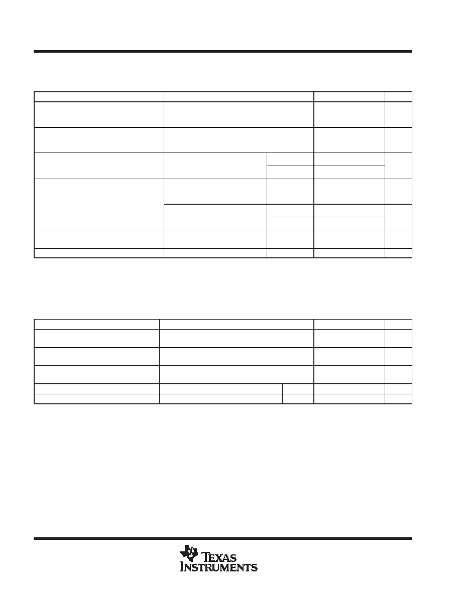
MSP430x13x, MSP430x14x, MSP430x14x1
MIXED SIGNAL MICROCONTROLLER
SLAS272F - JULY 2000 - REVISED JUNE 2004
34
POST OFFICE BOX 655303
∑
DALLAS, TEXAS 75265
electrical characteristics over recommended operating free-air temperature (unless otherwise
noted) (continued)
12-bit ADC, power supply and input range conditions (see Note 1)
PARAMETER
TEST CONDITIONS
MIN
NOM
MAX
UNIT
AVCC
Analog supply voltage
AVCC and DVCC are connected together
AVSS and DVSS are connected together
V(AVSS) = V(DVSS) = 0 V
2.2
3.6
V
V(P6.x/Ax)
Analog input voltage
range (see Note 2)
All P6.0/A0 to P6.7/A7 terminals. Analog inputs
selected in ADC12MCTLx register and P6Sel.x=1
0
x
7; V(AVSS)
VP6.x/Ax
V(AVCC)
0
VAVCC
V
IADC12
Operating supply current
into AVCC terminal
fADC12CLK = 5.0 MHz
ADC12ON = 1, REFON = 0
2.2 V
0.65
1.3
mA
IADC12
into AVCC terminal
(see Note 3)
ADC12CLK
ADC12ON = 1, REFON = 0
SHT0=0, SHT1=0, ADC12DIV=0
3 V
0.8
1.6
mA
IREF+
Operating supply current
into AVCC terminal
fADC12CLK = 5.0 MHz
ADC12ON = 0,
REFON = 1, REF2_5V = 1
3 V
0.5
0.8
mA
IREF+
into AVCC terminal
(see Note 4)
fADC12CLK = 5.0 MHz
ADC12ON = 0,
2.2 V
0.5
0.8
mA
(see Note 4)
ADC12CLK
ADC12ON = 0,
REFON = 1, REF2_5V = 0
3 V
0.5
0.8
mA
CI
Input capacitance
Only one terminal can be selected
at one time, P6.x/Ax
2.2 V
40
pF
RI
Input MUX ON resistance
0V
VAx
VAVCC
3 V
2000
Not production tested, limits verified by design
NOTES:
1. The leakage current is defined in the leakage current table with P6.x/Ax parameter.
2. The analog input voltage range must be within the selected reference voltage range VR+ to VR- for valid conversion results.
3. The internal reference supply current is not included in current consumption parameter IADC12.
4. The internal reference current is supplied via terminal AVCC. Consumption is independent of the ADC12ON control bit, unless a
conversion is active. The REFON bit enables to settle the built-in reference before starting an A/D conversion.
12-bit ADC, external reference (see Note 1)
PARAMETER
TEST CONDITIONS
MIN
NOM
MAX
UNIT
VeREF+
Positive external
reference voltage input
VeREF+ > VREF-/VeREF- (see Note 2)
1.4
VAVCC
V
VREF- /VeREF-
Negative external
reference voltage input
VeREF+ > VREF-/VeREF- (see Note 3)
0
1.2
V
(VeREF+ -
VREF-/VeREF-)
Differential external
reference voltage input
VeREF+ > VREF-/VeREF- (see Note 4)
1.4
VAVCC
V
IVeREF+
Static input current
0V
VeREF+
VAVCC
2.2 V/3 V
±
1
µ
A
IVREF-/VeREF-
Static input current
0V
VeREF-
VAVCC
2.2 V/3 V
±
1
µ
A
NOTES:
1. The external reference is used during conversion to charge and discharge the capacitance array. The input capacitance, Ci, is also
the dynamic load for an external reference during conversion. The dynamic impedance of the reference supply should follow the
recommendations on analog-source impedance to allow the charge to settle for 12-bit accuracy.
2. The accuracy limits the minimum positive external reference voltage. Lower reference voltage levels may be applied with reduced
accuracy requirements.
3. The accuracy limits the maximum negative external reference voltage. Higher reference voltage levels may be applied with reduced
accuracy requirements.
4. The accuracy limits minimum external differential reference voltage. Lower differential reference voltage levels may be applied with
reduced accuracy requirements.
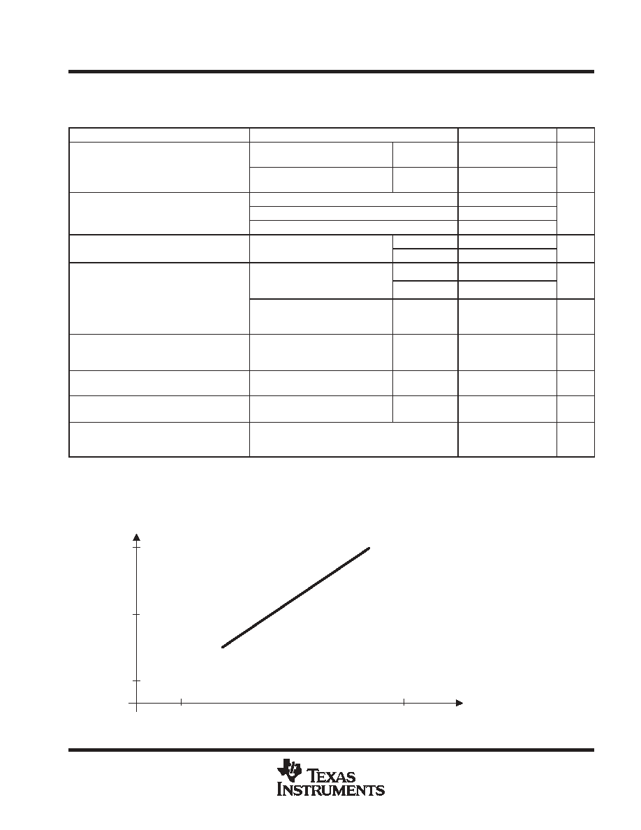
MSP430x13x, MSP430x14x, MSP430x14x1
MIXED SIGNAL MICROCONTROLLER
SLAS272F - JULY 2000 - REVISED JUNE 2004
35
POST OFFICE BOX 655303
∑
DALLAS, TEXAS 75265
electrical characteristics over recommended operating free-air temperature (unless otherwise
noted) (continued)
12-bit ADC, built-in reference
PARAMETER
TEST CONDITIONS
MIN
NOM
MAX
UNIT
VREF+
Positive built-in reference
REF2_5V = 1 for 2.5 V
IVREF+
IVREF+max
3 V
2.4
2.5
2.6
V
VREF+
Positive built-in reference
voltage output
REF2_5V = 0 for 1.5 V
IVREF+
IVREF+max
2.2 V/3 V
1.44
1.5
1.56
V
AVCC minimum voltage,
REF2_5V = 0, IVREF+
1mA
2.2
AVCC(min)
AVCC minimum voltage,
Positive built-in reference
active
REF2_5V = 1, IVREF+
0.5mA
VREF+ + 0.15
V
AVCC(min)
Positive built-in reference
active
REF2_5V = 1, IVREF+
1mA
VREF+ + 0.15
V
IVREF+
Load current out of VREF+
2.2 V
0.01
-0.5
mA
IVREF+
Load current out of VREF+
terminal
3 V
-1
mA
IVREF+ = 500
µ
A +/- 100
µ
A
Analog input voltage ~0.75 V;
2.2 V
±
2
LSB
IL(VREF)+
Load-current regulation
VREF+
Analog input voltage ~0.75 V;
REF2_5V = 0
3 V
±
2
LSB
IL(VREF)+
Load-current regulation
VREF+ terminal
IVREF+ = 500
µ
A
±
100
µ
A
Analog input voltage ~1.25 V;
REF2_5V = 1
3 V
±
2
LSB
IDL(VREF) +
Load current regulation
IVREF+ =100
µ
A
900
µ
A,
CVREF+=5
µ
F, ax ~0.5 x VREF+
3 V
20
ns
IDL(VREF) +
Load current regulation
VREF+ terminal
VREF+
CVREF+=5
µ
F, ax ~0.5 x VREF+
Error of conversion result
1 LSB
3 V
20
ns
CVREF+
Capacitance at pin VREF+
(see Note 1)
REFON =1,
0 mA
IVREF+
IVREF+max
2.2 V/3 V
5
10
µ
F
TREF+
Temperature coefficient of
built-in reference
IVREF+ is a constant in the range of
0 mA
IVREF+
1 mA
2.2 V/3 V
±
100
ppm/
∞
C
tREFON
Settle time of internal
reference voltage (see
Figure 13 and Note 2)
IVREF+ = 0.5 mA, CVREF+ = 10
µ
F,
VREF+ = 1.5 V, VAVCC = 2.2 V
17
ms
Not production tested, limits characterized
Not production tested, limits verified by design
NOTES:
1. The internal buffer operational amplifier and the accuracy specifications require an external capacitor. All INL and DNL tests uses
two capacitors between pins VREF+ and AVSS and VREF-/VeREF- and AVSS: 10
µ
F tantalum and 100 nF ceramic.
NOTES:
2. The condition is that the error in a conversion started after tREFON is less than
±
0.5 LSB. The settling time depends on the external
capacitive load.
CVREF+
1
µ
F
0
1 ms
10 ms
100 ms
tREFON
tREFON
.66 x CVREF+ [ms] with CVREF+ in
µ
F
100
µ
F
10
µ
F
Figure 13. Typical Settling Time of Internal Reference t
REFON
vs External Capacitor on V
REF
+
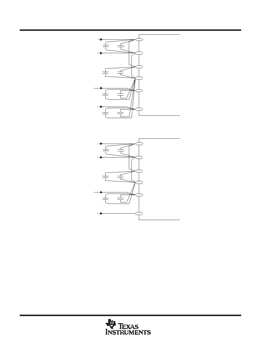
MSP430x13x, MSP430x14x, MSP430x14x1
MIXED SIGNAL MICROCONTROLLER
SLAS272F - JULY 2000 - REVISED JUNE 2004
36
POST OFFICE BOX 655303
∑
DALLAS, TEXAS 75265
+
-
10
µ
F
100 nF
AVSS
MSP430F13x
MSP430F14x
+
-
+
-
10
µ
F
100 nF
10
µ
F
100 nF
AVCC
10
µ
F
100 nF
DVSS
DVCC
From
Power
Supply
Apply
External
Reference
+
-
Apply External Reference [VeREF+]
or Use Internal Reference [VREF+]
VREF+ or VeREF+
VREF-/VeREF-
Figure 14. Supply Voltage and Reference Voltage Design V
REF-/
V
eREF-
External Supply
+
-
10
µ
F
100 nF
AVSS
MSP430F13x
MSP430F14x
+
-
10
µ
F
100 nF
AVCC
10
µ
F
100 nF
DVSS
DVCC
From
Power
Supply
+
-
Apply External Reference [VeREF+]
or Use Internal Reference [VREF+]
VREF+ or VeREF+
VREF-/VeREF-
Reference Is Internally
Switched to AVSS
Figure 15. Supply Voltage and Reference Voltage Design V
REF-/
V
eREF-
= AV
SS
, Internally Connected
MSP430x13x, MSP430x14x, MSP430x14x1
MIXED SIGNAL MICROCONTROLLER
SLAS272F - JULY 2000 - REVISED JUNE 2004
37
POST OFFICE BOX 655303
∑
DALLAS, TEXAS 75265
electrical characteristics over recommended operating free-air temperature (unless otherwise
noted) (continued)
12-bit ADC, timing parameters
PARAMETER
TEST CONDITIONS
MIN
NOM
MAX
UNIT
fADC12CLK
For specified performance of ADC12
linearity parameters
2.2V/
3V
0.45
5
6.3
MHz
fADC12OSC
Internal ADC12
oscillator
ADC12DIV=0,
fADC12CLK=fADC12OSC
2.2 V/
3V
3.7
6.3
MHz
tCONVERT
Conversion time
CVREF+
5
µ
F, Internal oscillator,
fADC12OSC = 3.7 MHz to 6.3 MHz
2.2 V/
3 V
2.06
3.51
µ
s
tCONVERT
Conversion time
External fADC12CLK from ACLK, MCLK or SMCLK:
ADC12SSEL
0
13
◊
ADC12DIV
◊
1/fADC12CLK
µ
s
tADC12ON
Turn on settling time of
the ADC
(see Note 1)
100
ns
tSample
Sampling time
RS = 400
, RI = 1000
,
CI = 30 pF
3 V
1220
ns
tSample
Sampling time
S
I
CI = 30 pF
= [RS + RI] x CI;(see Note 2)
2.2 V
1400
ns
Not production tested, limits characterized
Not production tested, limits verified by design
NOTES:
1. The condition is that the error in a conversion started after tADC12ON is less than
±
0.5 LSB. The reference and input signal are already
settled.
2. Approximately ten Tau (
) are needed to get an error of less than
±
0.5 LSB:
tSample = ln(2n+1) x (RS + RI) x CI+ 800 ns where n = ADC resolution = 12, RS = external source resistance.
12-bit ADC, linearity parameters
PARAMETER
TEST CONDITIONS
MIN
NOM
MAX
UNIT
EI
Integral linearity error
1.4 V
(VeREF+ - VREF-/VeREF-) min
1.6 V
2.2 V/3 V
±
2
LSB
EI
Integral linearity error
1.6 V < (VeREF+ - VREF-/VeREF-) min
[V(AVCC)]
2.2 V/3 V
±
1.7
LSB
ED
Differential linearity
error
(VeREF+ - VREF-/VeREF-)min
(VeREF+ - VREF-/VeREF-),
CVREF+ = 10
µ
F (tantalum) and 100 nF (ceramic)
2.2 V/3 V
±
1
LSB
EO
Offset error
(VeREF+ - VREF-/VeREF-)min
(VeREF+ - VREF-/VeREF-),
Internal impedance of source RS < 100
,
CVREF+ = 10
µ
F (tantalum) and 100 nF (ceramic)
2.2 V/3 V
±
2
±
4
LSB
EG
Gain error
(VeREF+ - VREF-/VeREF-)min
(VeREF+ - VREF-/VeREF-),
CVREF+ = 10
µ
F (tantalum) and 100 nF (ceramic)
2.2 V/3 V
±
1.1
±
2
LSB
ET
Total unadjusted
error
(VeREF+ - VREF-/VeREF-)min
(VeREF+ - VREF-/VeREF-),
CVREF+ = 10
µ
F (tantalum) and 100 nF (ceramic)
2.2 V/3 V
±
2
±
5
LSB
MSP430x13x, MSP430x14x, MSP430x14x1
MIXED SIGNAL MICROCONTROLLER
SLAS272F - JULY 2000 - REVISED JUNE 2004
38
POST OFFICE BOX 655303
∑
DALLAS, TEXAS 75265
electrical characteristics over recommended operating free-air temperature (unless otherwise
noted) (continued)
12-bit ADC, temperature sensor and built-in V
MID
PARAMETER
TEST CONDITIONS
MIN
NOM
MAX
UNIT
ISENSOR
Operating supply current into
REFON = 0, INCH = 0Ah,
2.2 V
40
120
A
ISENSOR
Operating supply current into
AVCC terminal (see Note 1)
REFON = 0, INCH = 0Ah,
ADC12ON=NA, TA = 25
_
C
3 V
60
160
µ
A
VSENSOR
ADC12ON = 1, INCH = 0Ah,
2.2 V
986
986
±
5%
mV
VSENSOR
ADC12ON = 1, INCH = 0Ah,
TA = 0
∞
C
3 V
986
986
±
5%
mV
TCSENSOR
ADC12ON = 1, INCH = 0Ah
2.2 V
3.55
3.55
±
3%
mV/
∞
C
TCSENSOR
ADC12ON = 1, INCH = 0Ah
3 V
3.55
3.55
±
3%
mV/
∞
C
tSENSOR(sample)
Sample time required if channel
ADC12ON = 1, INCH = 0Ah,
2.2 V
30
s
tSENSOR(sample)
Sample time required if channel
10 is selected (see Note 2)
ADC12ON = 1, INCH = 0Ah,
Error of conversion result
1 LSB
3 V
30
µ
s
IVMID
Current into divider at channel 11
ADC12ON = 1, INCH = 0Bh
2.2 V
NA
A
IVMID
Current into divider at channel 11
(see Note 3)
ADC12ON = 1, INCH = 0Bh
3 V
NA
µ
A
VMID
AVCC divider at channel 11
ADC12ON = 1, INCH = 0Bh,
2.2 V
1.1
1.1
±
0.04
V
VMID
AVCC divider at channel 11
ADC12ON = 1, INCH = 0Bh,
VMID is ~0.5 x VAVCC
3 V
1.5
1.50
±
0.04
V
tVMID(sample)
Sample time required if channel
ADC12ON = 1, INCH = 0Bh,
2.2 V
1400
ns
tVMID(sample)
Sample time required if channel
11 is selected (see Note 4)
ADC12ON = 1, INCH = 0Bh,
Error of conversion result
1 LSB
3 V
1220
ns
Not production tested, limits characterized
NOTES:
1. The sensor current ISENSOR is consumed if (ADC12ON = 1 and REFON=1), or (ADC12ON=1 AND INCH=0Ah and sample signal
is high). Therefore it includes the constant current through the sensor and the reference.
2. The typical equivalent impedance of the sensor is 51 k
. The sample time required includes the sensor-on time tSENSOR(on).
3. No additional current is needed. The VMID is used during sampling.
4. The on-time tVMID(on) is included in the sampling time tVMID(sample); no additional on time is needed.
MSP430x13x, MSP430x14x, MSP430x14x1
MIXED SIGNAL MICROCONTROLLER
SLAS272F - JULY 2000 - REVISED JUNE 2004
39
POST OFFICE BOX 655303
∑
DALLAS, TEXAS 75265
electrical characteristics over recommended operating free-air temperature (unless otherwise
noted) (continued)
Flash Memory
PARAMETER
TEST
CONDITIONS
VCC
MIN
NOM
MAX
UNIT
VCC(PGM/
ERASE)
Program and Erase supply voltage
2.7
3.6
V
fFTG
Flash Timing Generator frequency
257
476
kHz
IPGM
Supply current from DVCC during program
2.7 V/ 3.6 V
3
5
mA
IERASE
Supply current from DVCC during erase
2.7 V/ 3.6 V
3
7
mA
tCPT
Cumulative program time
see Note 1
2.7 V/ 3.6 V
4
ms
tCMErase
Cumulative mass erase time
see Note 2
2.7 V/ 3.6 V
200
ms
Program/Erase endurance
104
105
cycles
tRetention
Data retention duration
TJ = 25
∞
C
100
years
tWord
Word or byte program time
35
tBlock, 0
Block program time for 1st byte or word
30
tBlock, 1-63
Block program time for each additional byte or word
see Note 3
21
tFTG
tBlock, End
Block program end-sequence wait time
see Note 3
6
tFTG
tMass Erase
Mass erase time
5297
tSeg Erase
Segment erase time
4819
NOTES:
1. The cumulative program time must not be exceeded when writing to a 64-byte flash block. This parameter applies to all programming
methods: individual word/byte write and block write modes.
2. The mass erase duration generated by the flash timing generator is at least 11.1ms ( = 5297x1/fFTG,max = 5297x1/476kHz). To
achieve the required cumulative mass erase time the Flash Controller's mass erase operation can be repeated until this time is met.
(A worst case minimum of 19 cycles are required).
3. These values are hardwired into the Flash Controller's state machine (tFTG = 1/fFTG).
JTAG Interface
PARAMETER
TEST
CONDITIONS
VCC
MIN
NOM
MAX
UNIT
fTCK
TCK input frequency
see Note 1
2.2 V
0
5
MHz
fTCK
TCK input frequency
see Note 1
3 V
0
10
MHz
RInternal
Internal pull-up resistance on TMS, TCK, TDI/TCLK
see Note 2
2.2 V/ 3 V
25
60
90
k
NOTES:
1. fTCK may be restricted to meet the timing requirements of the module selected.
2. TMS, TDI/TCLK, and TCK pull-up resistors are implemented in all versions.
JTAG Fuse (see Note 1)
PARAMETER
TEST
CONDITIONS
VCC
MIN
NOM
MAX
UNIT
VCC(FB)
Supply voltage during fuse-blow condition
TA = 25
∞
C
2.5
V
VFB
Voltage level on TDI/TCLK for fuse-blow: F versions
6
7
V
IFB
Supply current into TDI/TCLK during fuse blow
100
mA
tFB
Time to blow fuse
1
ms
NOTES:
1. Once the fuse is blown, no further access to the MSP430 JTAG/Test and emulation features is possible. The JTAG block is switched
to bypass mode.
MSP430x13x, MSP430x14x, MSP430x14x1
MIXED SIGNAL MICROCONTROLLER
SLAS272F - JULY 2000 - REVISED JUNE 2004
40
POST OFFICE BOX 655303
∑
DALLAS, TEXAS 75265
APPLICATION INFORMATION
input/output schematic
port P1, P1.0 to P1.7, input/output with Schmitt-trigger
P1.0/TACLK ..
P1IN.x
Module X IN
Pad Logic
Interrupt
Flag
Edge
Select
Interrupt
P1SEL.x
P1IES.x
P1IFG.x
P1IE.x
P1IRQ.x
EN
D
Set
EN
Q
P1OUT.x
P1DIR.x
P1SEL.x
Module X OUT
Direction Control
From Module
0
1
0
1
P1.7/TA2
PnSel.x
PnDIR.x
Dir. CONTROL
FROM MODULE
PnOUT.x
MODULE X OUT
PnIN.x
MODULE X IN
PnIE.x
PnIFG.x
PnIES.x
P1Sel.0
P1DIR.0
P1DIR.0
P1OUT.0
DVSS
P1IN.0
TACLK
P1IE.0
P1IFG.0
P1IES.0
P1Sel.1
P1DIR.1
P1DIR.1
P1OUT.1
Out0 signal
P1IN.1
CCI0A
P1IE.1
P1IFG.1
P1IES.1
P1Sel.2
P1DIR.2
P1DIR.2
P1OUT.2
Out1 signal
P1IN.2
CCI1A
P1IE.2
P1IFG.2
P1IES.2
P1Sel.3
P1DIR.3
P1DIR.3
P1OUT.3
Out2 signal
P1IN.3
CCI2A
P1IE.3
P1IFG.3
P1IES.3
P1Sel.4
P1DIR.4
P1DIR.4
P1OUT.4
SMCLK
P1IN.4
unused
P1IE.4
P1IFG.4
P1IES.4
P1Sel.5
P1DIR.5
P1DIR.5
P1OUT.5
Out0 signal
P1IN.5
unused
P1IE.5
P1IFG.5
P1IES.5
P1Sel.6
P1DIR.6
P1DIR.6
P1OUT.6
Out1 signal
P1IN.6
unused
P1IE.6
P1IFG.6
P1IES.6
P1Sel.7
P1DIR.7
P1DIR.7
P1OUT.7
Out2 signal
P1IN.7
unused
P1IE.7
P1IFG.7
P1IES.7
Signal from or to Timer_A
MSP430x13x, MSP430x14x, MSP430x14x1
MIXED SIGNAL MICROCONTROLLER
SLAS272F - JULY 2000 - REVISED JUNE 2004
41
POST OFFICE BOX 655303
∑
DALLAS, TEXAS 75265
APPLICATION INFORMATION
input/output schematic (continued)
port P2, P2.0 to P2.2, P2.6, and P2.7 input/output with Schmitt-trigger
P2IN.x
P2OUT.x
Pad Logic
P2DIR.x
P2SEL.x
Module X OUT
Edge
Select
Interrupt
P2SEL.x
P2IES.x
P2IFG.x
P2IE.x
P2IRQ.x
Direction Control
P2.0/ACLK
0
1
0
1
Interrupt
Flag
Set
EN
Q
Module X IN
EN
D
Bus Keeper
CAPD.X
P2.1/TAINCLK
P2.2/CAOUT/TA0
P2.6/ADC12CLK
P2.7/TA0
0: Input
1: Output
x: Bit Identifier 0 to 2, 6, and 7 for Port P2
From Module
PnSel.x
PnDIR.x
Dir. CONTROL
FROM MODULE
PnOUT.x
MODULE X OUT
PnIN.x
MODULE X IN
PnIE.x
PnIFG.x
PnIES.x
P2Sel.0
P2DIR.0
P2DIR.0
P2OUT.0
ACLK
P2IN.0
unused
P2IE.0
P2IFG.0
P2IES.0
P2Sel.1
P2DIR.1
P2DIR.1
P2OUT.1
DVSS
P2IN.1
INCLK
P2IE.1
P2IFG.1
P2IES.1
P2Sel.2
P2DIR.2
P2DIR.2
P2OUT.2
CAOUT
P2IN.2
CCI0B
P2IE.2
P2IFG.2
P2IES.2
P2Sel.6
P2DIR.6
P2DIR.6
P2OUT.6
ADC12CLK∂
P2IN.6
unused
P2IE.6
P2IFG.6
P2IES.6
P2Sel.7
P2DIR.7
P2DIR.7
P2OUT.7
Out0 signalß
P2IN.7
unused
P2IE.7
P2IFG.7
P2IES.7
Signal from Comparator_A
Signal to Timer_A
ß Signal from Timer_A
∂ ADC12CLK signal is output of the 12-bit ADC module
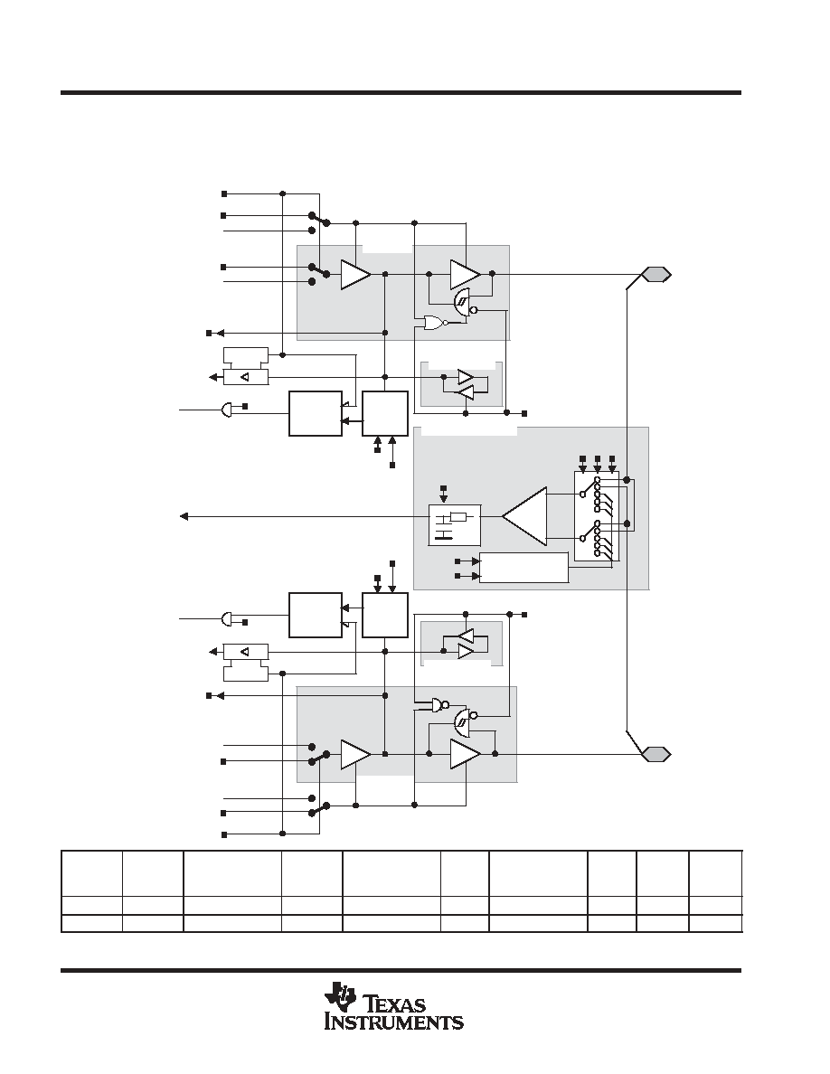
MSP430x13x, MSP430x14x, MSP430x14x1
MIXED SIGNAL MICROCONTROLLER
SLAS272F - JULY 2000 - REVISED JUNE 2004
42
POST OFFICE BOX 655303
∑
DALLAS, TEXAS 75265
APPLICATION INFORMATION
input/output schematic (continued)
port P2, P2.3 to P2.4, input/output with Schmitt-trigger
Bus Keeper
P2IN.3
P2OUT.3
Pad Logic
P2DIR.3
P2SEL.3
Module X OUT
Edge
Select
Interrupt
P2SEL.3
P2IES.3
P2IFG.3
P2IE.3
P2IRQ.3
Direction Control
From Module
P2.3/CA0/TA1
0
1
0
1
Interrupt
Flag
Set
EN
Q
Module X IN
EN
D
P2IN.4
P2OUT.4
Pad Logic
P2DIR.4
P2SEL.4
Module X OUT
Edge
Select
Interrupt
P2SEL.4
P2IES.4
P2IFG.4
P2IE.4
P2IRQ.4
Direction Control
From Module
P2.4/CA1/TA2
0
1
0
1
Interrupt
Flag
Set
EN
Q
Module X IN
EN
D
Comparator_A
-
+
Reference Block
CCI1B
CAF
CAREF
P2CA
CAEX
CAREF
Bus Keeper
CAPD.3
CAPD.4
To Timer_A3
0: Input
1: Output
0: Input
1: Output
PnSel.x
PnDIR.x
DIRECTION
CONTROL
FROM MODULE
PnOUT.x
MODULE X OUT
PnIN.x
MODULE X IN
PnIE.x
PnIFG.x
PnIES.x
P2Sel.3
P2DIR.3
P2DIR.3
P2OUT.3
Out1 signal
P2IN.3
unused
P2IE.3
P2IFG.3
P2IES.3
P2Sel.4
P2DIR.4
P2DIR.4
P2OUT.4
Out2 signal
P2IN.4
unused
P2IE.4
P2IFG.4
P2IES.4
Signal from Timer_A
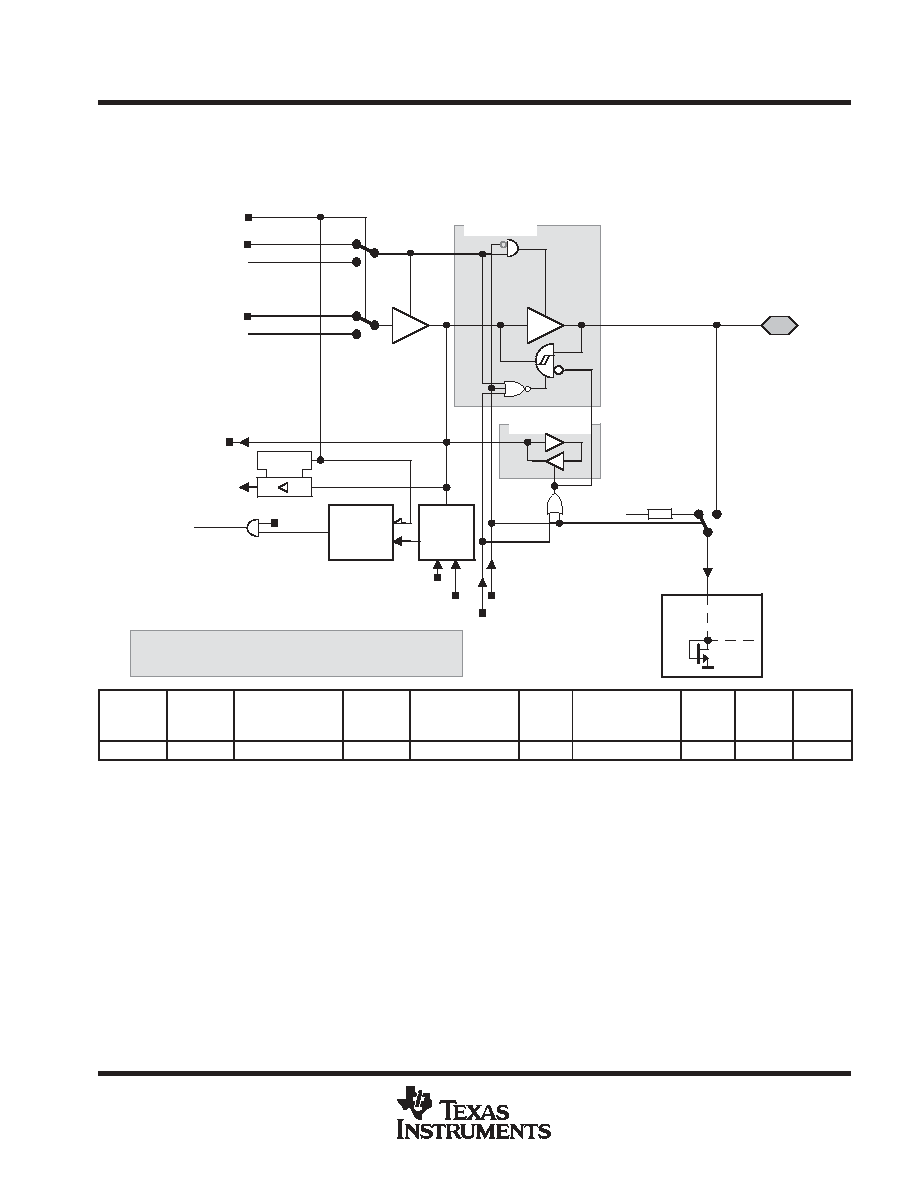
MSP430x13x, MSP430x14x, MSP430x14x1
MIXED SIGNAL MICROCONTROLLER
SLAS272F - JULY 2000 - REVISED JUNE 2004
43
POST OFFICE BOX 655303
∑
DALLAS, TEXAS 75265
APPLICATION INFORMATION
input/output schematic (continued)
port P2, P2.5, input/output with Schmitt-trigger and R
osc
function for the basic clock module
P2IN.5
P2OUT.5
Pad Logic
P2DIR.5
P2SEL.5
Module X OUT
Edge
Select
Interrupt
P2SEL.5
P2IES.5
P2IFG.5
P2IE.5
P2IRQ.5
Direction Control
P2.5/Rosc
0
1
0
1
Interrupt
Flag
Set
EN
Q
DCOR
Module X IN
EN
D
to
0
1
DC Generator
Bus Keeper
CAPD.5
DCOR: Control Bit From Basic Clock Module
If it Is Set, P2.5 Is Disconnected From P2.5 Pad
Internal to
Basic Clock
Module
VCC
0: Input
1: Output
From Module
PnSel.x
PnDIR.x
DIRECTION
CONTROL
FROM MODULE
PnOUT.x
MODULE X OUT
PnIN.x
MODULE X IN
PnIE.x
PnIFG.x
PnIES.x
P2Sel.5
P2DIR.5
P2DIR.5
P2OUT.5
DVSS
P2IN.5
unused
P2IE.5
P2IFG.5
P2IES.5
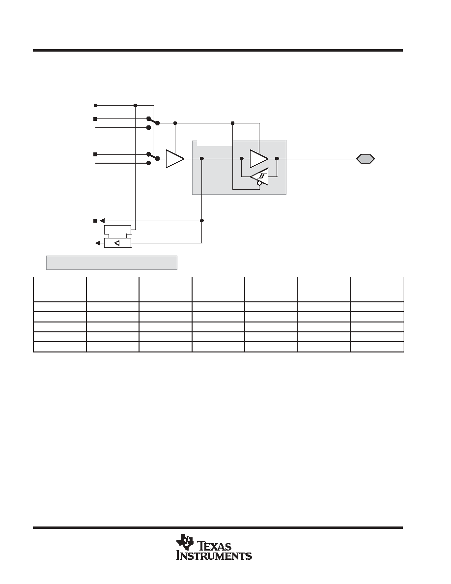
MSP430x13x, MSP430x14x, MSP430x14x1
MIXED SIGNAL MICROCONTROLLER
SLAS272F - JULY 2000 - REVISED JUNE 2004
44
POST OFFICE BOX 655303
∑
DALLAS, TEXAS 75265
APPLICATION INFORMATION
input/output schematic (continued)
port P3, P3.0 and P3.4 to P3.7, input/output with Schmitt-trigger
P3.0/STE0
P3IN.x
Module X IN
Pad Logic
EN
D
P3OUT.x
P3DIR.x
P3SEL.x
Module X OUT
Direction Control
From Module
0
1
0
1
P3.4/UTXD0
P3.5/URXD0
0: Input
1: Output
x: Bit Identifier, 0 and 4 to 7 for Port P3
P3.6/UTXD1
P3.7/URXD1∂
PnSel.x
PnDIR.x
DIRECTION
CONTROL
FROM MODULE
PnOUT.x
MODULE X OUT
PnIN.x
MODULE X IN
P3Sel.0
P3DIR.0
DVSS
P3OUT.0
DVSS
P3IN.0
STE0
P3Sel.4
P3DIR.4
DVCC
P3OUT.4
UTXD0
P3IN.4
Unused
P3Sel.5
P3DIR.5
DVSS
P3OUT.5
DVSS
P3IN.5
URXD0ß
P3Sel.6
P3DIR.6
DVCC
P3OUT.6
UTXD1
P3IN.6
Unused
P3Sel.7
P3DIR.7
DVSS
P3OUT.7
DVSS
P3IN.7
URXD1
∂
Output from USART0 module
Output from USART1 module in x14x(1) configuration, DVSS in x13x configuration
ß Input to USART0 module
∂ Input to USART1 module in x14x(1) configuration, unused in x13x configuration
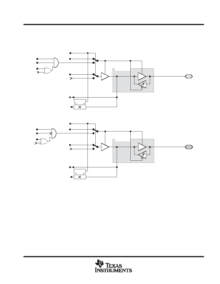
MSP430x13x, MSP430x14x, MSP430x14x1
MIXED SIGNAL MICROCONTROLLER
SLAS272F - JULY 2000 - REVISED JUNE 2004
45
POST OFFICE BOX 655303
∑
DALLAS, TEXAS 75265
APPLICATION INFORMATION
input/output schematic (continued)
port P3, P3.1, input/output with Schmitt-trigger
P3.1/SIMO0
P3IN.1
Pad Logic
EN
D
P3OUT1
P3DIR.1
P3SEL.1
(SI)MO0
0
1
0
1
DCM_SIMO
SYNC
MM
STE
STC
From USART0
SI(MO)0
To USART0
0: Input
1: Output
port P3, P3.2, input/output with Schmitt-trigger
P3.2/SOMI0
P3IN.2
Pad Logic
EN
D
P3OUT.2
P3DIR.2
P3SEL.2
0
1
0
1
DCM_SOMI
SYNC
MM
STE
STC
SO(MI)0
From USART0
(SO)MI0
To USART0
0: Input
1: Output
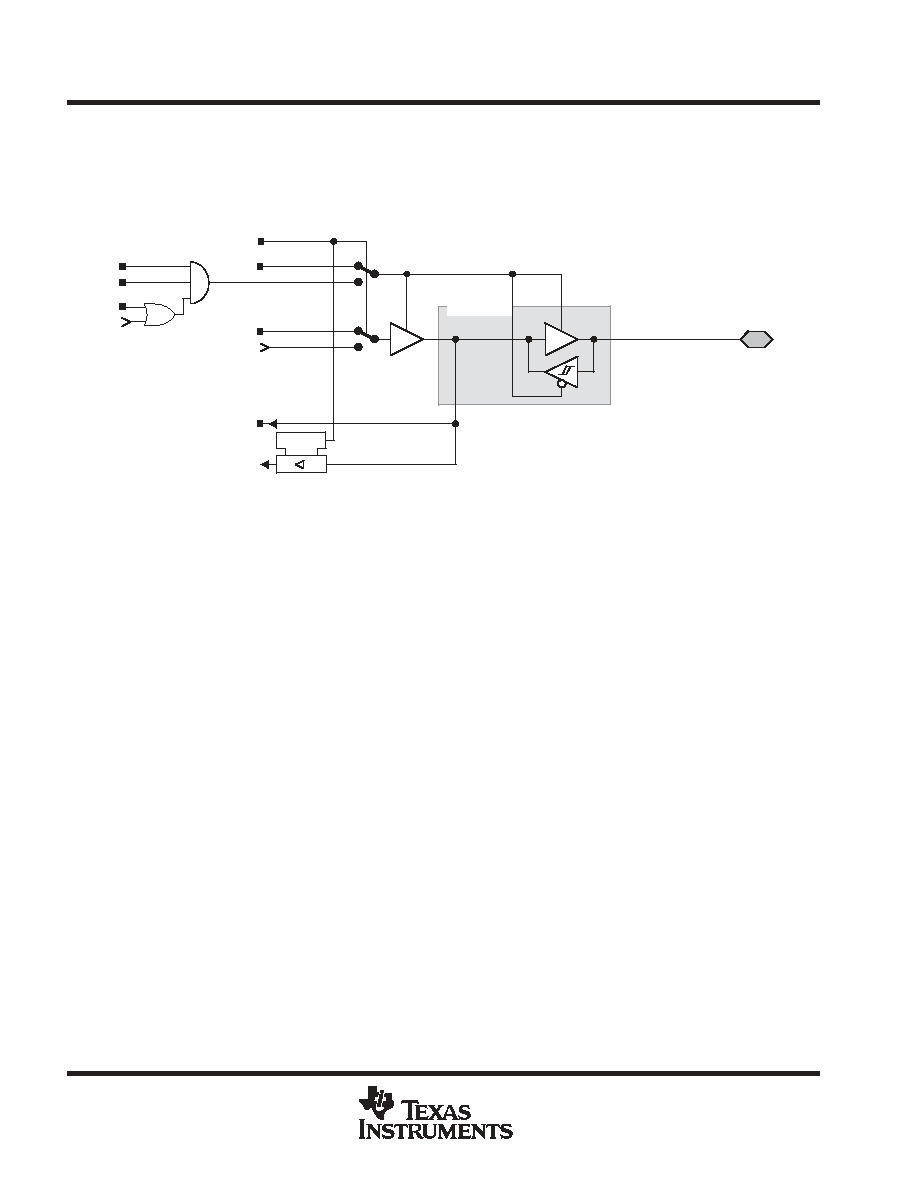
MSP430x13x, MSP430x14x, MSP430x14x1
MIXED SIGNAL MICROCONTROLLER
SLAS272F - JULY 2000 - REVISED JUNE 2004
46
POST OFFICE BOX 655303
∑
DALLAS, TEXAS 75265
APPLICATION INFORMATION
input/output schematic (continued)
port P3, P3.3, input/output with Schmitt-trigger
P3.3/UCLK0
P3IN.3
Pad Logic
EN
D
P3OUT.3
P3DIR.3
P3SEL.3
UCLK.0
0
1
0
1
DCM_UCLK
SYNC
MM
STE
STC
From USART0
UCLK0
To USART0
0: Input
1: Output
NOTE: UART mode:
The UART clock can only be an input. If UART mode and UART function are selected, the P3.3/UCLK0 is always
an input.
SPI, slave mode:
The clock applied to UCLK0 is used to shift data in and out.
SPI, master mode:
The clock to shift data in and out is supplied to connected devices on pin P3.3/UCLK0 (in slave mode).
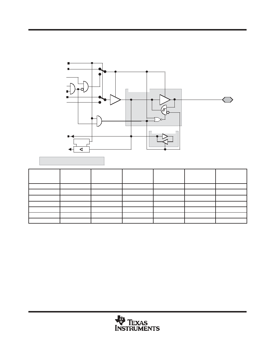
MSP430x13x, MSP430x14x, MSP430x14x1
MIXED SIGNAL MICROCONTROLLER
SLAS272F - JULY 2000 - REVISED JUNE 2004
47
POST OFFICE BOX 655303
∑
DALLAS, TEXAS 75265
APPLICATION INFORMATION
input/output schematic (continued)
port P4, P4.0 to P4.6, input/output with Schmitt-trigger
P4.0/TB0 ..
P4IN.x
Module X IN
Pad Logic
EN
D
x: bit identifier, 0 to 6 for Port P4
P4OUT.x
P4DIR.x
P4SEL.x
Module X OUT
Direction Control
From Module
0
1
0
1
Bus Keeper
TBOUTHiZ
P4.6/TB6
0: Input
1: Output
P5SEL.7
Module X IN
w
PnSel.x
PnDIR.x
DIRECTION
CONTROL
FROM MODULE
PnOUT.x
MODULE X OUT
PnIN.x
MODULE X IN
P4Sel.0
P4DIR.0
P4DIR.0
P4OUT.0
Out0 signal
P4IN.0
CCI0A / CCI0B
P4Sel.1
P4DIR.1
P4DIR.1
P4OUT.1
Out1 signal
P4IN.1
CCI1A / CCI1B
P4Sel.2
P4DIR.2
P4DIR.2
P4OUT.2
Out2 signal
P4IN.2
CCI2A / CCI2B
P4Sel.3
P4DIR.3
P4DIR.3
P4OUT.3
Out3 signal
P4IN.3
CCI3A / CCI3B
P4Sel.4
P4DIR.4
P4DIR.4
P4OUT.4
Out4 signal
P4IN.4
CCI4A / CCI4B
P4Sel.5
P4DIR.5
P4DIR.5
P4OUT.5
Out5 signal
P4IN.5
CCI5A / CCI5B
P4Sel.6
P4DIR.6
P4DIR.6
P4OUT.6
Out6 signal
P4IN.6
CCI6A
Signal from Timer_B
Signal to Timer_B
ß From P5.7
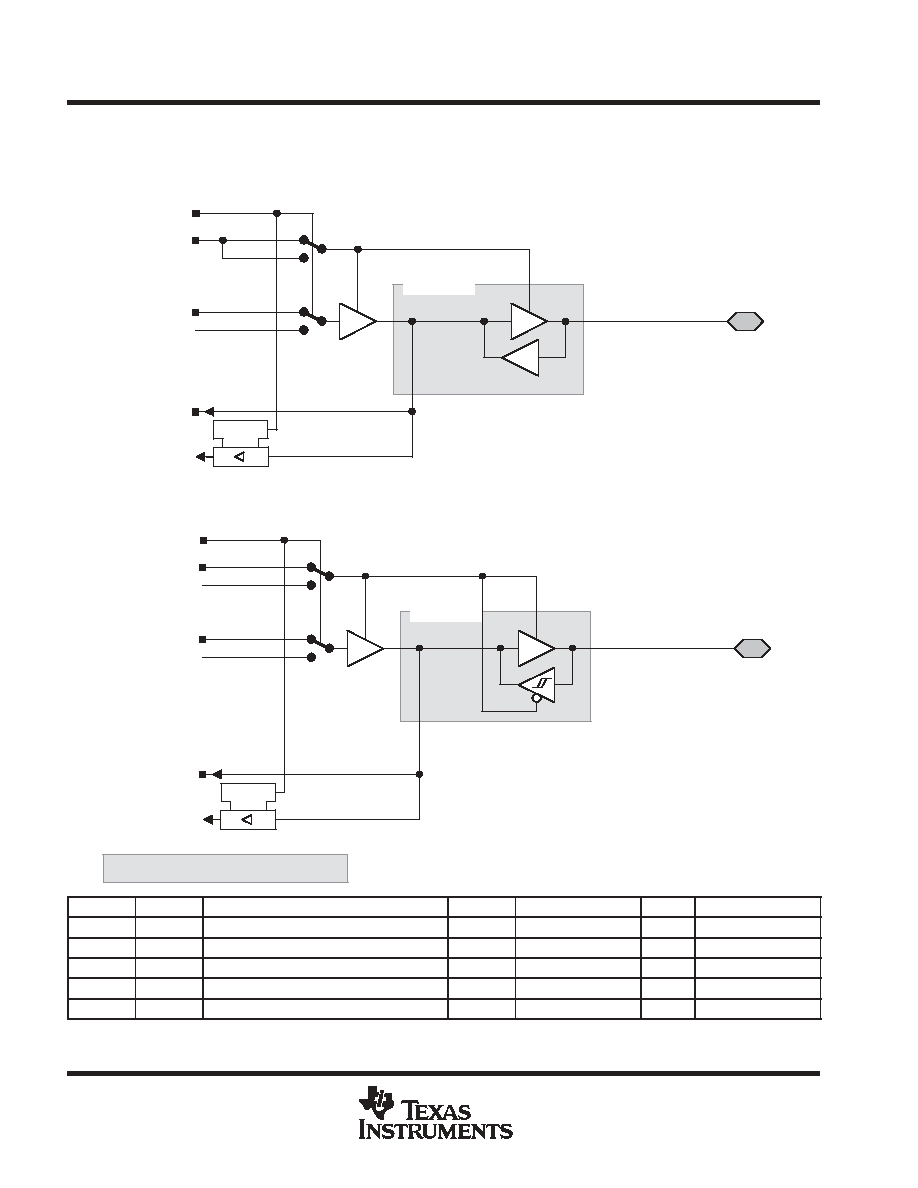
MSP430x13x, MSP430x14x, MSP430x14x1
MIXED SIGNAL MICROCONTROLLER
SLAS272F - JULY 2000 - REVISED JUNE 2004
48
POST OFFICE BOX 655303
∑
DALLAS, TEXAS 75265
APPLICATION INFORMATION
input/output schematic (continued)
port P4, P4.7, input/output with Schmitt-trigger
P4.7/TBCLK
P4IN.7
Timer_B,
Pad Logic
EN
D
P4OUT.7
P4DIR.7
P4SEL.7
0
1
0
1
TBCLK
0: Input
1: Output
DVSS
port P5, P5.0 and P5.4 to P5.7, input/output with Schmitt-trigger
P5.0/STE1
P5IN.x
Module X IN
Pad Logic
EN
D
P5OUT.x
P5DIR.x
P5SEL.x
Module X OUT
Direction Control
From Module
0
1
0
1
P5.4/MCLK
P5.5/SMCLK
P5.6/ACLK
P5.7/TBOUTH
x: Bit Identifier, 0 and 4 to 7 for Port P5
0: Input
1: Output
PnSel.x
PnDIR.x
Dir. CONTROL FROM MODULE
PnOUT.x
MODULE X OUT
PnIN.x
MODULE X IN
P5Sel.0
P5DIR.0
DVSS
P5OUT.0
DVSS
P5IN.0
STE.1
P5Sel.4
P5DIR.4
DVCC
P5OUT.4
MCLK
P5IN.4
unused
P5Sel.5
P5DIR.5
DVCC
P5OUT.5
SMCLK
P5IN.5
unused
P5Sel.6
P5DIR.6
DVCC
P5OUT.6
ACLK
P5IN.6
unused
P5Sel.7
P5DIR.7
DVSS
P5OUT.7
DVSS
P5IN.7
TBOUTHiZ
NOTE: TBOUTHiZ signal is used by port module P4, pins P4.0 to P4.6. The function of TBOUTHiZ is mainly useful when used with Timer_B7.
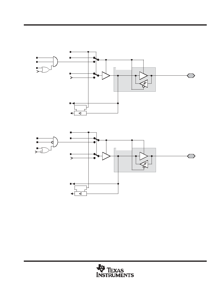
MSP430x13x, MSP430x14x, MSP430x14x1
MIXED SIGNAL MICROCONTROLLER
SLAS272F - JULY 2000 - REVISED JUNE 2004
49
POST OFFICE BOX 655303
∑
DALLAS, TEXAS 75265
APPLICATION INFORMATION
input/output schematic (continued)
port P5, P5.1, input/output with Schmitt-trigger
P5.1/SIMO1
P5IN.1
Pad Logic
EN
D
P5OUT.1
P5DIR.1
P5SEL.1
0
1
0
1
DCM_SIMO
SYNC
MM
STE
STC
(SI)MO1
From USART1
SI(MO)1
To USART1
0: Input
1: Output
port P5, P5.2, input/output with Schmitt-trigger
P5.2/SOMI1
P5IN.2
Pad Logic
EN
D
P5OUT.2
P5DIR.2
P5SEL.2
0
1
0
1
DCM_SOMI
SYNC
MM
STE
STC
SO(MI)1
From USART1
(SO)MI1
To USART1
0: Input
1: Output
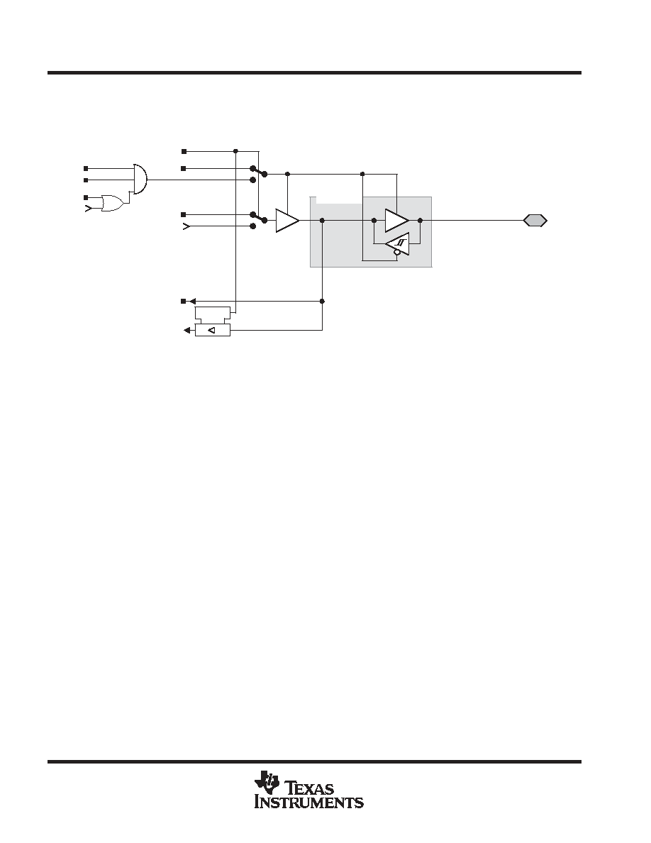
MSP430x13x, MSP430x14x, MSP430x14x1
MIXED SIGNAL MICROCONTROLLER
SLAS272F - JULY 2000 - REVISED JUNE 2004
50
POST OFFICE BOX 655303
∑
DALLAS, TEXAS 75265
APPLICATION INFORMATION
input/output schematic (continued)
port P5, P5.3, input/output with Schmitt-trigger
P5.3/UCLK1
P5IN.3
Pad Logic
EN
D
P5OUT.3
P5DIR.3
P5SEL.3
0
1
0
1
DCM_SIMO
SYNC
MM
STE
STC
UCLK1
From USART1
UCLK1
To USART1
0: Input
1: Output
NOTE: UART mode:
The UART clock can only be an input. If UART mode and UART function are selected, the P5.3/UCLK1 direction
is always input.
SPI, slave mode:
The clock applied to UCLK1 is used to shift data in and out.
SPI, master mode:
The clock to shift data in and out is supplied to connected devices on pin P5.3/UCLK1 (in slave mode).
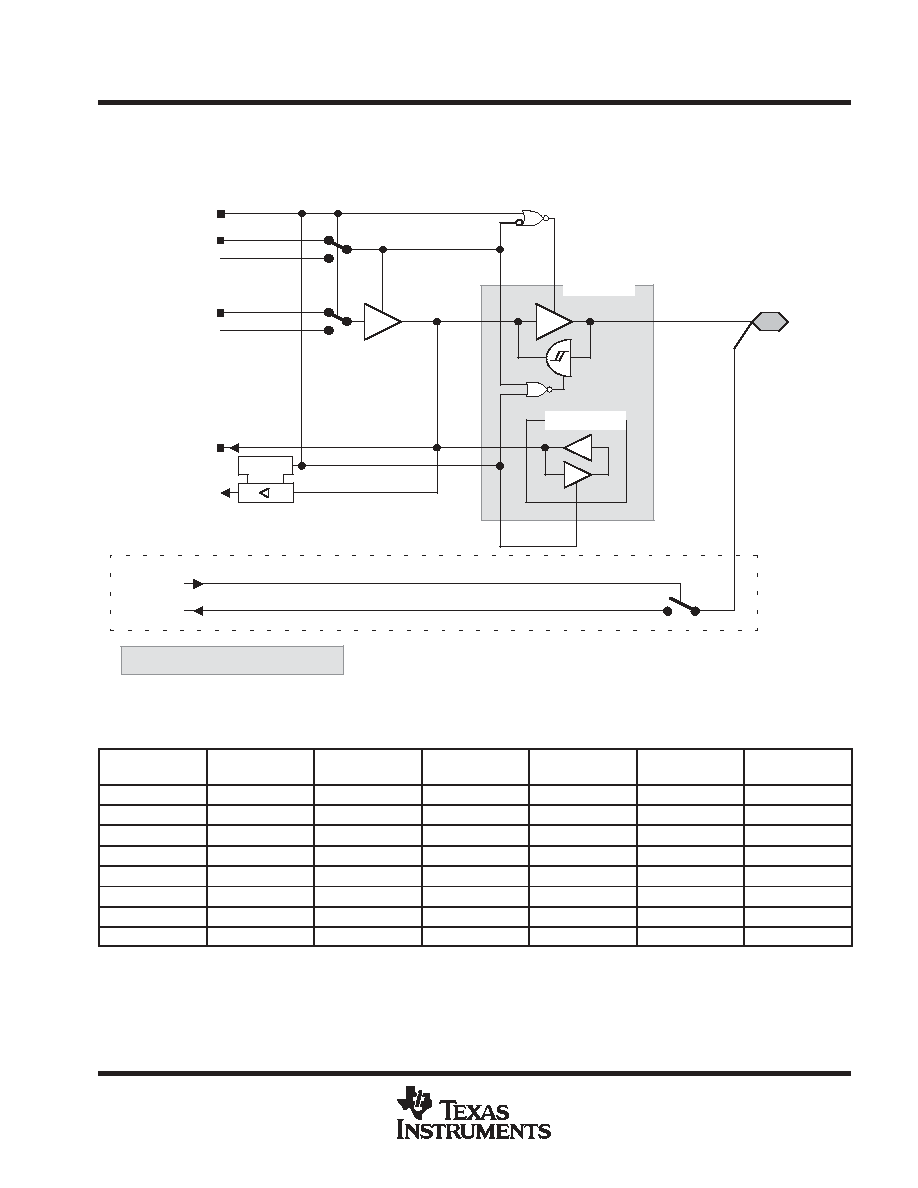
MSP430x13x, MSP430x14x, MSP430x14x1
MIXED SIGNAL MICROCONTROLLER
SLAS272F - JULY 2000 - REVISED JUNE 2004
51
POST OFFICE BOX 655303
∑
DALLAS, TEXAS 75265
APPLICATION INFORMATION
input/output schematic (continued)
port P6, P6.0 to P6.7, input/output with Schmitt-trigger
P6.0 .. P6.7
P6IN.x
Module X IN
Pad Logic
EN
D
P6OUT.x
P6DIR.x
P6SEL.x
Module X OUT
Direction Control
From Module
0
1
0
1
Bus Keeper
To ADC
From ADC
0: Input
1: Output
x: Bit Identifier, 0 to 7 for Port P6
Note: Not implemented in the MSP430x14x1 devices
NOTE: Analog signals applied to digital gates can cause current flow from the positive to the negative terminal. The throughput current flows if
the analog signal is in the range of transitions 0
1 or 1
0. The value of the throughput current depends on the driving capability of the
gate. For MSP430, it is approximately 100
µ
A.
Use P6SEL.x=1 to prevent throughput current. P6SEL.x should be set, even if the signal at the pin is not being used by the ADC12.
PnSel.x
PnDIR.x
DIR. CONTROL
FROM MODULE
PnOUT.x
MODULE X OUT
PnIN.x
MODULE X IN
P6Sel.0
P6DIR.0
P6DIR.0
P6OUT.0
DVSS
P6IN.0
unused
P6Sel.1
P6DIR.1
P6DIR.1
P6OUT.1
DVSS
P6IN.1
unused
P6Sel.2
P6DIR.2
P6DIR.2
P6OUT.2
DVSS
P6IN.2
unused
P6Sel.3
P6DIR.3
P6DIR.3
P6OUT.3
DVSS
P6IN.3
unused
P6Sel.4
P6DIR.4
P6DIR.4
P6OUT.4
DVSS
P6IN.4
unused
P6Sel.5
P6DIR.5
P6DIR.5
P6OUT.5
DVSS
P6IN.5
unused
P6Sel.6
P6DIR.6
P6DIR.6
P6OUT.6
DVSS
P6IN.6
unused
P6Sel.7
P6DIR.7
P6DIR.7
P6OUT.7
DVSS
P6IN.7
unused
NOTE: The signal at pins P6.x/Ax is used by the 12-bit ADC module.
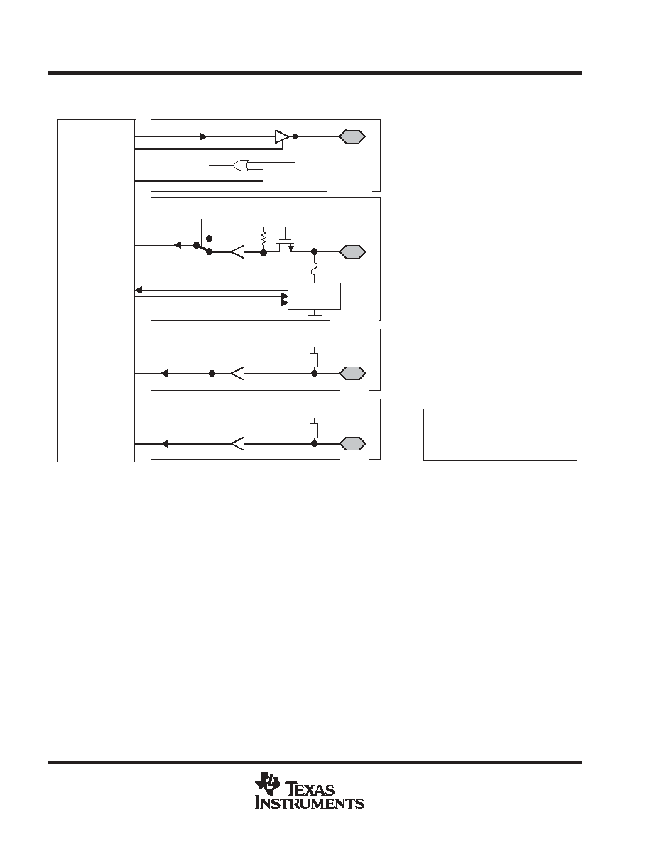
MSP430x13x, MSP430x14x, MSP430x14x1
MIXED SIGNAL MICROCONTROLLER
SLAS272F - JULY 2000 - REVISED JUNE 2004
52
POST OFFICE BOX 655303
∑
DALLAS, TEXAS 75265
APPLICATION INFORMATION
JTAG pins TMS, TCK, TDI/TCLK, TDO/TDI, input/output with Schmitt-trigger
TDI
TDO
TMS
TCK
Test
JTAG
&
Emulation
Module
Burn & Test
Fuse
Controlled by JTAG
Controlled by JTAG
Controlled
by JTAG
DVCC
DVCC
DVCC
During Programming Activity and
During Blowing of the Fuse, Pin
TDO/TDI Is Used to Apply the Test
Input Data for JTAG Circuitry
TDO/TDI
TDI/TCLK
TMS
TCK
Fuse
DVCC
MSP430x13x, MSP430x14x, MSP430x14x1
MIXED SIGNAL MICROCONTROLLER
SLAS272F - JULY 2000 - REVISED JUNE 2004
53
POST OFFICE BOX 655303
∑
DALLAS, TEXAS 75265
APPLICATION INFORMATION
JTAG fuse check mode
MSP430 devices that have the fuse on the TDI/TCLK terminal have a fuse check mode that tests the continuity
of the fuse the first time the JTAG port is accessed after a power-on reset (POR). When activated, a fuse check
current, I
TF
, of 1 mA at 3 V, 2.5 mA at 5 V can flow from the TDI/TCLK pin to ground if the fuse is not burned.
Care must be taken to avoid accidentally activating the fuse check mode and increasing overall system power
consumption.
Activation of the fuse check mode occurs with the first negative edge on the TMS pin after power up or if the
TMS is being held low during power up. The second positive edge on the TMS pin deactivates the fuse check
mode. After deactivation, the fuse check mode remains inactive until another POR occurs. After each POR the
fuse check mode has the potential to be activated.
The fuse check current will only flow when the fuse check mode is active and the TMS pin is in a low state (see
Figure 16). Therefore, the additional current flow can be prevented by holding the TMS pin high (default
condition).
Time TMS Goes Low After POR
TMS
ITF
ITDI/TCLK
Figure 16. Fuse Check Mode Current: MSP430F13x, MSP430F14x(1)
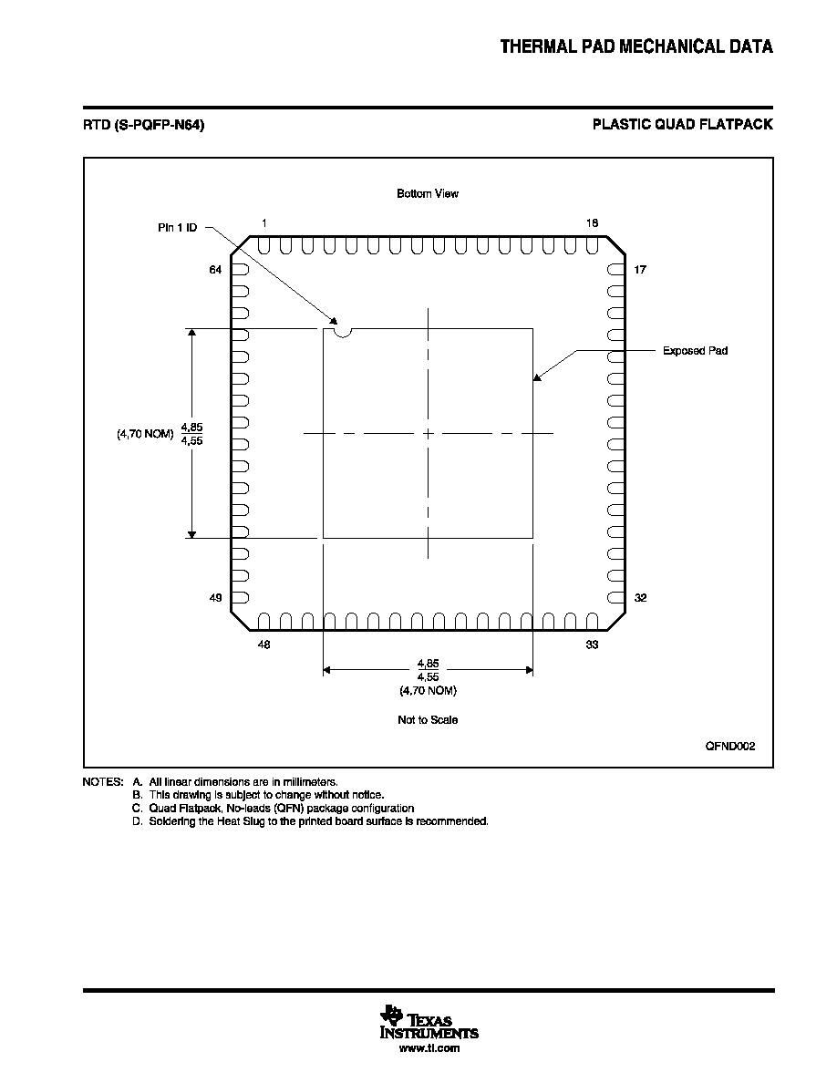
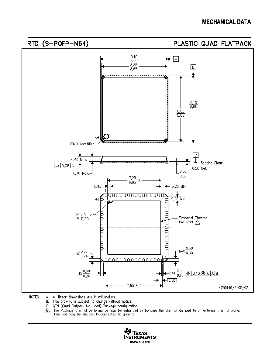

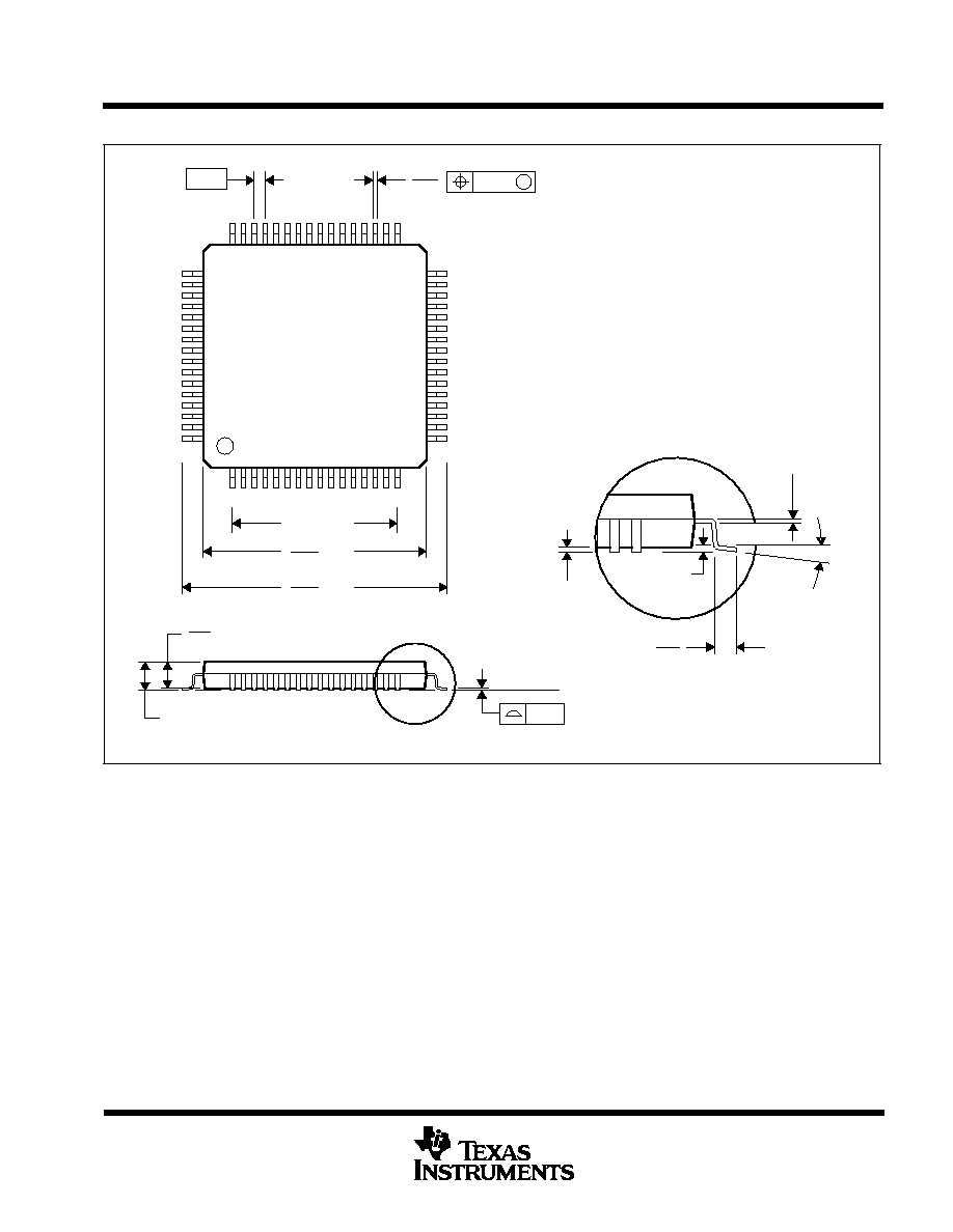
MECHANICAL DATA
MTQF006A ≠ JANUARY 1995 ≠ REVISED DECEMBER 1996
1
POST OFFICE BOX 655303
∑
DALLAS, TEXAS 75265
PAG (S-PQFP-G64)
PLASTIC QUAD FLATPACK
0,13 NOM
0,25
0,45
0,75
Seating Plane
0,05 MIN
4040282 / C 11/96
Gage Plane
33
0,17
0,27
16
48
1
7,50 TYP
49
64
SQ
9,80
1,05
0,95
11,80
12,20
1,20 MAX
10,20
SQ
17
32
0,08
0,50
M
0,08
0
∞
≠ 7
∞
NOTES: A. All linear dimensions are in millimeters.
B. This drawing is subject to change without notice.
C. Falls within JEDEC MS-026
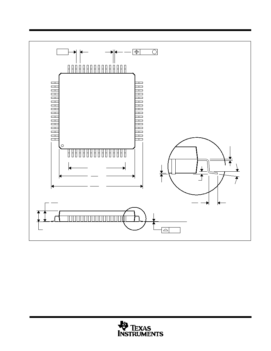
MECHANICAL DATA
MTQF008A ≠ JANUARY 1995 ≠ REVISED DECEMBER 1996
1
POST OFFICE BOX 655303
∑
DALLAS, TEXAS 75265
PM (S-PQFP-G64)
PLASTIC QUAD FLATPACK
4040152 / C 11/96
32
17
0,13 NOM
0,25
0,45
0,75
Seating Plane
0,05 MIN
Gage Plane
0,27
33
16
48
1
0,17
49
64
SQ
SQ
10,20
11,80
12,20
9,80
7,50 TYP
1,60 MAX
1,45
1,35
0,08
0,50
M
0,08
0
∞
≠ 7
∞
NOTES: A. All linear dimensions are in millimeters.
B. This drawing is subject to change without notice.
C. Falls within JEDEC MS-026
D. May also be thermally enhanced plastic with leads connected to the die pads.

IMPORTANT NOTICE
Texas Instruments Incorporated and its subsidiaries (TI) reserve the right to make corrections, modifications,
enhancements, improvements, and other changes to its products and services at any time and to discontinue
any product or service without notice. Customers should obtain the latest relevant information before placing
orders and should verify that such information is current and complete. All products are sold subject to TI's terms
and conditions of sale supplied at the time of order acknowledgment.
TI warrants performance of its hardware products to the specifications applicable at the time of sale in
accordance with TI's standard warranty. Testing and other quality control techniques are used to the extent TI
deems necessary to support this warranty. Except where mandated by government requirements, testing of all
parameters of each product is not necessarily performed.
TI assumes no liability for applications assistance or customer product design. Customers are responsible for
their products and applications using TI components. To minimize the risks associated with customer products
and applications, customers should provide adequate design and operating safeguards.
TI does not warrant or represent that any license, either express or implied, is granted under any TI patent right,
copyright, mask work right, or other TI intellectual property right relating to any combination, machine, or process
in which TI products or services are used. Information published by TI regarding third-party products or services
does not constitute a license from TI to use such products or services or a warranty or endorsement thereof.
Use of such information may require a license from a third party under the patents or other intellectual property
of the third party, or a license from TI under the patents or other intellectual property of TI.
Reproduction of information in TI data books or data sheets is permissible only if reproduction is without
alteration and is accompanied by all associated warranties, conditions, limitations, and notices. Reproduction
of this information with alteration is an unfair and deceptive business practice. TI is not responsible or liable for
such altered documentation.
Resale of TI products or services with statements different from or beyond the parameters stated by TI for that
product or service voids all express and any implied warranties for the associated TI product or service and
is an unfair and deceptive business practice. TI is not responsible or liable for any such statements.
Following are URLs where you can obtain information on other Texas Instruments products and application
solutions:
Products
Applications
Amplifiers
amplifier.ti.com
Audio
www.ti.com/audio
Data Converters
dataconverter.ti.com
Automotive
www.ti.com/automotive
DSP
dsp.ti.com
Broadband
www.ti.com/broadband
Interface
interface.ti.com
Digital Control
www.ti.com/digitalcontrol
Logic
logic.ti.com
Military
www.ti.com/military
Power Mgmt
power.ti.com
Optical Networking
www.ti.com/opticalnetwork
Microcontrollers
microcontroller.ti.com
Security
www.ti.com/security
Telephony
www.ti.com/telephony
Video & Imaging
www.ti.com/video
Wireless
www.ti.com/wireless
Mailing Address:
Texas Instruments
Post Office Box 655303 Dallas, Texas 75265
Copyright
2004, Texas Instruments Incorporated