Document Outline
- features
- description
- device pinout
- functional block diagram
- Terminal Functions
- short-form description
- CPU
- instruction set
- operating modes
- interrupt vector addresses
- special function registers
- interrupt enable 1 and 2
- interrupt flag register 1 and 2
- memory organization
- bootstrap loader (BSL)
- flash memory
- peripherals
- oscillator and system clock
- brownout
- digital I/O
- WDT+ watchdog timer
- comparator_A+
- timer_A3
- peripheral file map
- absolute maximum ratingsÅ
- recommended operating conditions
- electrical characteristics over recommended ranges of supply voltage and operating free-air temperature ( unless otherwise noted)
- supply current (into VCC) excluding external current ( see Notes 1 and 2)
- typical supply current (into VCC) characteristics
- Schmitt-trigger inputs - Ports P1 and P2
- inputs - Ports P1 and P2
- leakage current - Ports P1 and P2
- outputs - Ports P1 and P2
- output frequency - Ports P1 and P2
- Timer_A
- Comparator_A+ (see Note 1)
- typical characteristics
- typical resistance between CA+ and CA- with CASHORT = 1
- POR/brownout reset (BOR) (see Note 1)
- typical characteristics
- main DCO characteristics
- DCO frequency
- DCO drift
- wake-up from lower power modes (LPM3/4)
- typical wake-up time characteristics
- crystal oscillator, LFXT1
- typical operating areas for oscillator LFXT1 in HF mode (XTS = 1)
- Flash Memory
- RAM
- JTAG Interface
- JTAG Fuse (see Note 1)
- APPLICATION INFORMATION
- Port P1 pin schematic: P1.0 to P1.3, input/output with Schmitt-trigger
- Port P1 pin schematic: P1.4 to P1.7, input/output with Schmitt-trigger and in-system access features
- Port P2 pin schematic: P2.0 to P2.5, input/output with Schmitt-trigger
- Port P2 pin schematic: P2.6, input/output with Schmitt-trigger and crystal oscillator input
- Port P2 pin schematic: P2.7, input/output with Schmitt-trigger and crystal oscillator output
- MECHANICAL DATA
- DW (R-PDSO-G**) PLASTIC SMALL-OUTLINE PACKAGE
- PW (R-PDSO-G**) PLASTIC SMALL-OUTLINE PACKAGE
- DGV (R-PDSO-G**) PLASTIC SMALL-OUTLINE
- RGE (S-PQFP-N24) PLASTIC QUAD FLATPACK
- IMPORTANT NOTICE
MSP430x21x1
MIXED SIGNAL MICROCONTROLLER
SLAS439 - SEPTEMBER 2004
1
POST OFFICE BOX 655303
∑
DALLAS, TEXAS 75265
D
Low Supply Voltage Range 1.8 V to 3.6 V
D
Ultralow-Power Consumption
- Active Mode: 200
µ
A at 1 MHz, 2.2 V
- Standby Mode: 0.7
µ
A
- Off Mode (RAM Retention): 0.1
µ
A
D
Ultrafast Wake-Up From Standby Mode in
less than 1
µ
s
D
16-Bit RISC Architecture, 65 ns
Instruction Cycle Time
D
Basic Clock Module Configurations:
- Internal Frequencies up to 16MHz
- 32-kHz Crystal
- High-Frequency Crystal up to 16MHz
- Resonator
- External Clock Source
D
16-Bit Timer_A With Three
Capture/Compare Registers
D
On-Chip Comparator for Analog Signal
Compare Function or Slope A/D
Conversion
D
Serial Onboard Programming,
No External Programming Voltage Needed
Programmable Code Protection by
Security Fuse
D
Bootstrap Loader in Flash Devices
D
Family Members Include:
MSP430F2101: 1KB + 256B Flash Memory
128B RAM
MSP430F2111: 2KB + 256B Flash Memory
128B RAM
MSP430F2121: 4KB + 256B Flash Memory
256B RAM
MSP430F2131: 8KB + 256B Flash Memory
256B RAM
D
Available in a 20-Pin Plastic Small-Outline
Wide Body (SOWB) Package, 20-Pin Plastic
Small-Outline Thin (TSSOP) Package,
20-Pin TVSOP and 24-Pin QFN
D
For Complete Module Descriptions, Refer
to the MSP430x2xx Family User's Guide
description
The Texas Instruments MSP430 family of ultralow power microcontrollers consist of several devices featuring
different sets of peripherals targeted for various applications. The architecture, combined with five low power
modes is optimized to achieve extended battery life in portable measurement applications. The device features
a powerful 16-bit RISC CPU, 16-bit registers, and constant generators that attribute to maximum code efficiency.
The digitally controlled oscillator (DCO) allows wake-up from low-power modes to active mode in less than 1
µ
s.
The MSP430x21x1 series is an ultralow-power mixed signal microcontroller with a built-in 16-bit timer, versatile
analog comparator and sixteen I/O pins.
Typical applications include sensor systems that capture analog signals, convert them to digital values, and then
process the data for display or for transmission to a host system. Stand alone RF sensor front end is another
area of application. The analog comparator provides slope A/D conversion capability.
AVAILABLE OPTIONS
PACKAGED DEVICES
TA
PLASTIC
20-PIN SOWB
(DW)
PLASTIC
20-PIN TSSOP
(PW)
PLASTIC
20-PIN TVSOP
(DGV)
PLASTIC
24-PIN QFN
(RGE)
- 40
∞
C to 85
∞
C
MSP430F2101IDW
MSP430F2111IDW
MSP430F2101IPW
MSP430F2111IPW
MSP430F2101IDGV
MSP430F2111IDGV
MSP430F2101IRGE
MSP430F2111IRGE
- 40
∞
C to 85
∞
C
MSP430F2111IDW
MSP430F2121IDW
MSP430F2131IDW
MSP430F2111IPW
MSP430F2121IPW
MSP430F2131IPW
MSP430F2111IDGV
MSP430F2121IDGV
MSP430F2131IDGV
MSP430F2111IRGE
MSP430F2121IRGE
MSP430F2131IRGE
PRODUCT PREVIEW
Please be aware that an important notice concerning availability, standard warranty, and use in critical applications of
Texas Instruments semiconductor products and disclaimers thereto appears at the end of this data sheet.
Copyright
2004 Texas Instruments Incorporated
PRODUCT PREVIEW information concerns products in the formative or
design phase of development. Characteristic data and other
specifications are design goals. Texas Instruments reserves the right to
change or discontinue these products without notice.
MSP430x21x1
MIXED SIGNAL MICROCONTROLLER
SLAS439 - SEPTEMBER 2004
2
POST OFFICE BOX 655303
∑
DALLAS, TEXAS 75265
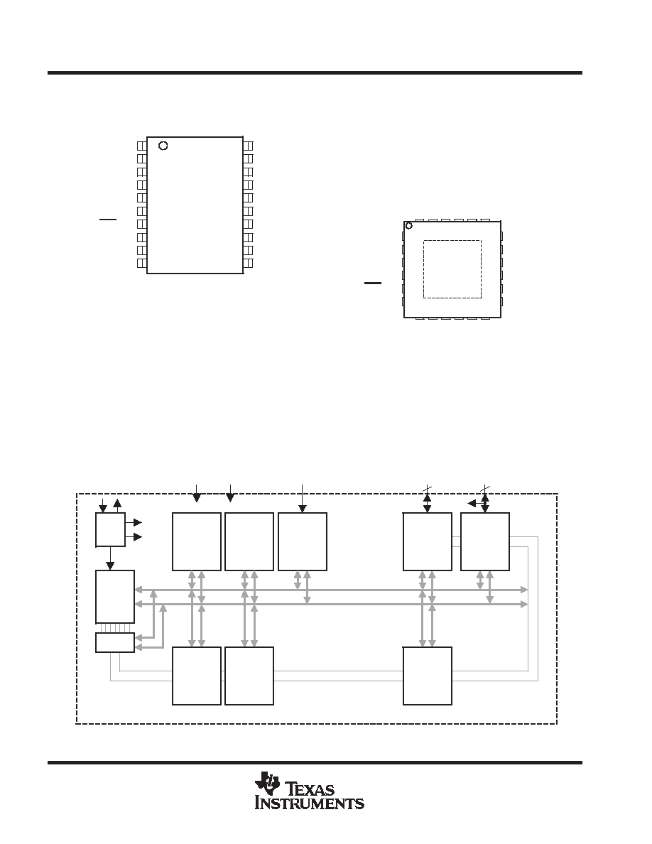
device pinout
RGE PACKAGE
(TOP VIEW)
DW, PW, or DGV PACKAGE
(TOP VIEW)
Note: NC pins not internally connected
Power Pad connection to VSS recommended
10
1
9
7
8
6
5
4
3
2
11
20
12
14
13
15
16
17
18
19
TEST
VCC
P2.5/CA5
VSS
XOUT/P2.7/CA7
XIN/P2.6/CA6
RST/NMI
P2.0/ACLK/CA2
P2.1/INCLK/CA3
P2.2/CAOUT/TA0/CA4
P1.7/TA2/TDO/TDI
P1.6/TA1/TDI/TCLK
P1.5/TA0/TMS
P1.3/TA2
P1.2/TA1
P1.1/TA0
P1.0/TACLK
P2.4/TA2/CA1
P2.3/TA1/CA0
P1.4/SMCLK/TCK
1
6
5
4
3
2
18
13
14
15
16
17
7
12
11
10
9
8
19
24 23 22 21 20
TEST
V
CC
P2.5/CA5
VSS
XOUT/P2.7/CA7
XIN/P2.6/CA6
RST/NMI
P2.0/ACLK/CA2
P2.1/INCLK/CA3
P2.2/CAOUT/T
A0/CA4
P1.7/T
A2/TDO/TDI
P1.6/T
A1/TDI/TCLK
P1.5/TA0/TMS
P1.3/TA2
P1.2/TA1
P1.1/TA0
P1.0/TACLK
P2.4/T
A2/CA1
P2.3/T
A1/CA0
P1.4/SMCLK/TCK
NC
NC
NC
NC
functional block diagram
Basic
Clock
8kB Flash
4kB Flash
2KB Flash
1KB Flash
256B RAM
256B RAM
128B RAM
128B RAM
Brownout
Protection
P1.x &
JTAG
P2.x &
XIN/XOUT
RST/NMI
VCC
VSS
MCLK
ACLK
SMCLK
XIN
XOUT
Note: See port schematics section for detailed I/O information
I/O Port P1
8 I/Os with
Interrupt
Capability
I/O Port P2
8 I/Os with
Interrupt
Capability
Watchdog
WDT+
15/16-Bit
Timer_A3
3 CC
Registers
Comparator_
A+
8 Channel
Input Mux
CPU &
Working
Registers
Emulation
XIN
XOUT
PRODUCT PREVIEW
MSP430x21x1
MIXED SIGNAL MICROCONTROLLER
SLAS439 - SEPTEMBER 2004
3
POST OFFICE BOX 655303
∑
DALLAS, TEXAS 75265
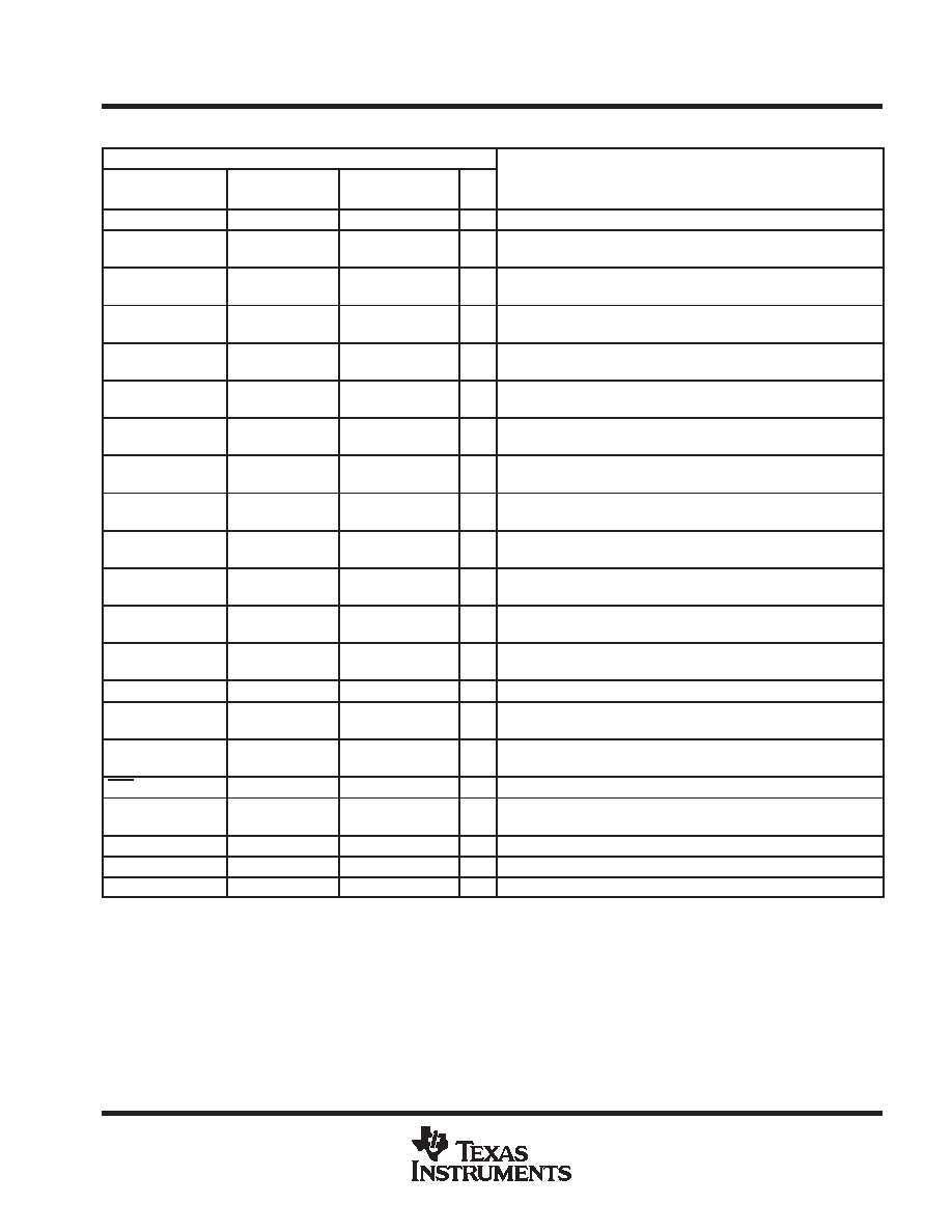
Terminal Functions
TERMINAL
NAME
DW, PW, or DGV
RGE
I/O
DESCRIPTION
NAME
NO.
NO.
I/O
DESCRIPTION
P1.0/TACLK
13
13
I/O
General-purpose digital I/O pin/Timer_A, clock signal TACLK input
P1.1/TA0
14
14
I/O
General-purpose digital I/O pin/Timer_A, capture: CCI0A input,
compare: Out0 output/BSL transmit
P1.2/TA1
15
15
I/O
General-purpose digital I/O pin/Timer_A, capture: CCI1A input,
compare: Out1 output
P1.3/TA2
16
16
I/O
General-purpose digital I/O pin/Timer_A, capture: CCI2A input,
compare: Out2 output
P1.4/SMCLK/TCK
17
17
I/O
General-purpose digital I/O pin/SMCLK signal output/test clock, input
terminal for device programming and test
P1.5/TA0/TMS
18
18
I/O
General-purpose digital I/O pin/Timer_A, compare: Out0 output/test
mode select, input terminal for device programming and test
P1.6/TA1/TDI/TCLK
19
20
I/O
General-purpose digital I/O pin/Timer_A, compare: Out1 output/test
data input or test clock input during programming and test
P1.7/TA2/TDO/TDI
20
21
I/O
General-purpose digital I/O pin/Timer_A, compare: Out2 output/test
data output terminal or test data input during programming and test
P2.0/ACLK/CA2
8
6
I/O
General-purpose digital I/O pin/ACLK output/comparator_A+, CA2
input
P2.1/INCLK/CA3
9
7
I/O
General-purpose digital I/O pin/Timer_A, clock signal at
INCLK/comparator_A+, CA3 input
P2.2/CAOUT/
TA0/CA4
10
8
I/O
General-purpose digital I/O pin/Timer_A, capture: CCI0B input/
comparator_A+, output/comparator_A+, CA4 input/BSL receive
P2.3/CA0/TA1
11
10
I/O
General-purpose digital I/O pin/Timer_A, compare: Out1 output/
comparator_A+, CA0 input
P2.4/CA1/TA2
12
11
I/O
General-purpose digital I/O pin/Timer_A, compare: Out2 output/
comparator_A+, CA1 input
P2.5/CA5
3
24
I/O
General-purpose digital I/O pin/ comparator_A+, CA5 input
XIN/P2.6/CA6
6
4
I/O
Input terminal of crystal oscillator/general-purpose digital I/O pin/
comparator_A+, CA6 input
XOUT/P2.7/CA7
5
3
I/O
Output terminal of crystal oscillator/general-purpose digital I/O pin/
comparator_A+, CA7 input
RST/NMI
7
5
I
Reset or nonmaskable interrupt input
TEST
1
22
I
Selects test mode for JTAG pins on Port1. The device protection fuse
is connected to TEST.
VCC
2
23
Supply voltage
VSS
4
2
Ground reference
QFN Pad
NA
Package Pad
NA
QFN package pad connection to VSS recommended.
TDO or TDI is selected via JTAG instruction.
NOTE:
If XOUT/P2.7/CA7 is used as an input, excess current will flow until P2SEL.7 is cleared. This is due to the oscillator output
driver connection to this pad after reset.
PRODUCT PREVIEW
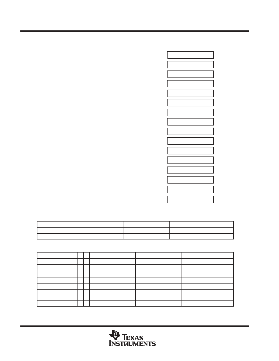
General-Purpose Register
Program Counter
Stack Pointer
Status Register
Constant Generator
General-Purpose Register
General-Purpose Register
General-Purpose Register
PC/R0
SP/R1
SR/CG1/R2
CG2/R3
R4
R5
R12
R13
General-Purpose Register
General-Purpose Register
R6
R7
General-Purpose Register
General-Purpose Register
R8
R9
General-Purpose Register
General-Purpose Register
R10
R11
General-Purpose Register
General-Purpose Register
R14
R15
MSP430x21x1
MIXED SIGNAL MICROCONTROLLER
SLAS439 - SEPTEMBER 2004
4
POST OFFICE BOX 655303
∑
DALLAS, TEXAS 75265
short-form description
CPU
The MSP430 CPU has a 16-bit RISC architecture
that is highly transparent to the application. All
operations, other than program-flow instructions,
are performed as register operations in
conjunction with seven addressing modes for
source operand and four addressing modes for
destination operand.
The CPU is integrated with 16 registers that
provide reduced instruction execution time. The
register-to-register operation execution time is
one cycle of the CPU clock.
Four of the registers, R0 to R3, are dedicated as
program counter, stack pointer, status register,
and constant generator respectively. The
remaining registers are general-purpose
registers.
Peripherals are connected to the CPU using data,
address, and control buses, and can be handled
with all instructions.
instruction set
The instruction set consists of 51 instructions with
three formats and seven address modes. Each
instruction can operate on word and byte data.
Table 1 shows examples of the three types of
instruction formats; the address modes are listed
in Table 2.
Table 1. Instruction Word Formats
Dual operands, source-destination
e.g. ADD R4,R5
R4 + R5 ---> R5
Single operands, destination only
e.g. CALL R8
PC -->(TOS), R8--> PC
Relative jump, un/conditional
e.g. JNE
Jump-on-equal bit = 0
Table 2. Address Mode Descriptions
ADDRESS MODE
S
D
SYNTAX
EXAMPLE
OPERATION
Register
F F
MOV Rs,Rd
MOV R10,R11
R10 --> R11
Indexed
F F
MOV X(Rn),Y(Rm)
MOV 2(R5),6(R6)
M(2+R5)--> M(6+R6)
Symbolic (PC relative)
F F
MOV EDE,TONI
M(EDE) --> M(TONI)
Absolute
F F
MOV &MEM,&TCDAT
M(MEM) --> M(TCDAT)
Indirect
F
MOV @Rn,Y(Rm)
MOV @R10,Tab(R6)
M(R10) --> M(Tab+R6)
Indirect
autoincrement
F
MOV @Rn+,Rm
MOV @R10+,R11
M(R10) --> R11
R10 + 2--> R10
Immediate
F
MOV #X,TONI
MOV #45,TONI
#45 --> M(TONI)
NOTE: S = source D = destination
PRODUCT PREVIEW

MSP430x21x1
MIXED SIGNAL MICROCONTROLLER
SLAS439 - SEPTEMBER 2004
5
POST OFFICE BOX 655303
∑
DALLAS, TEXAS 75265
operating modes
The MSP430 has one active mode and five software selectable low-power modes of operation. An interrupt
event can wake up the device from any of the five low-power modes, service the request and restore back to
the low-power mode on return from the interrupt program.
The following six operating modes can be configured by software:
D
Active mode AM;
-
All clocks are active
D
Low-power mode 0 (LPM0);
-
CPU is disabled
ACLK and SMCLK remain active. MCLK is disabled
D
Low-power mode 1 (LPM1);
-
CPU is disabled
ACLK and SMCLK remain active. MCLK is disabled
DCO's dc-generator is disabled if DCO not used in active mode
D
Low-power mode 2 (LPM2);
-
CPU is disabled
MCLK and SMCLK are disabled
DCO's dc-generator remains enabled
ACLK remains active
D
Low-power mode 3 (LPM3);
-
CPU is disabled
MCLK and SMCLK are disabled
DCO's dc-generator is disabled
ACLK remains active
D
Low-power mode 4 (LPM4);
-
CPU is disabled
ACLK is disabled
MCLK and SMCLK are disabled
DCO's dc-generator is disabled
Crystal oscillator is stopped
PRODUCT PREVIEW