Document Outline
- features
- description
- pin designation, MSP430x412, MSP430x413
- pin designation, MSP430x415, MSP430x417
- functional block diagram, MSP430x412, MSP430x413
- functional block diagram, MSP430x415, MSP430x417
- Terminal Functions
- MSP430x412, MSP430x413
- MSP430x415, MSP430x417
- short-form description
- CPU
- instruction set
- operating modes
- interrupt vector addresses
- special function registers
- interrupt enable 1 and 2
- interrupt flag register 1 and 2
- module enable registers 1 and 2
- memory organization
- bootstrap loader (BSL)
- flash memory
- peripherals
- oscillator and system clock
- brownout, supply voltage supervisor
- digital I/O
- Basic Timer1
- LCD drive
- watchdog timer
- comparator_A
- timer_A3/timer0_A3
- timer1_A5 (MSP430x415 and MSP430x417 only)
- peripheral file map
- absolute maximum ratingsÅ
- recommended operating conditions
- electrical characteristics over recommended operating free-air temperature (unless otherwise noted)
- supply current into AVCC + DVCC excluding external current, (see Note 1)
- current consumption of active mode versus system frequency, F version
- current consumption of active mode versus supply voltage, F version
- Schmitt-trigger inputs - Ports P1, P2, P3, P4, P5, and P6
- standard inputs - RST\/NMI; JTAG: TCK, TMS, TDI/TCLK, TDO/TDI
- inputs Px.x, TAx/TAx.x
- leakage current(see Note1)
- outputs - Ports P1, P2, P3, P4, P5, and P6
- output frequency
- MSP430x412, MSP430x413 outputs - Ports P1, P2, P3, P4, P5, and P6(see Note)
- MSP430x415, MSP430x417 outputs - Ports P1, P2, P3, P4, P5, and P6(see Note)
- wake-up LPM3
- RAM(see Note1)
- LCD
- Comparator_A(see Note 1)
- POR brownout, reset(see Notes 1 and 2)
- SVS (supply voltage supervisor/monitor) MSP430x412, MSP430x413 only
- SVS (supply voltage supervisor/monitor) MSP430x415, MSP430x417 only
- DCO
- crystal oscillator, LFXT1 oscillator(see Notes 1 and 2)
- Flash Memory
- JTAG Interface
- JTAG Fuse(see Note 1)
- APPLICATION INFORMATION
- input/output schematic
- Port P1, P1.0 to P1.5, input/output with Schmitt-trigger
- Port P1, P1.6, P1.7 input/output with Schmitt-trigger
- port P2, P2.0 to P2.7, input/output with Schmitt-trigger
- port P3, P3.0, P3.7, input/output with Schmitt-trigger
- port P4, P4.0 to P4.7, input/output with Schmitt-trigger
- port P5, P5.0, P5.1, input/output with Schmitt-trigger
- port P5, P5.2, P5.4, input/output with Schmitt-trigger
- port P5, P5.5 to P5.7, input/output with Schmitt-trigger
- port P6, P6.0 to P6.6, input/output with Schmitt-trigger
- port P6, P6.7 input/output with Schmitt-trigger
- port P6, P6.7 input/output with Schmitt-trigger
- JTAG pins TMS, TCK, TDI/TCLK, TDO/TDI, input/output with Schmitt-trigger or output
- JTAG fuse check mode
- THERMAL PAD MECHANICAL DATA
- RTD(S-PQFP-N64) PLASTIC QUAD FLATPACK
MSP430x41x
MIXED SIGNAL MICROCONTROLLER
SLAS340G - MAY 2001 - REVISED JUNE 2004
1
POST OFFICE BOX 655303
∑
DALLAS, TEXAS 75265
D
Low Supply-Voltage Range, 1.8 V . . . 3.6 V
D
Ultralow-Power Consumption:
- Active Mode: 200
µ
A at 1 MHz, 2.2 V
- Standby Mode: 0.7
µ
A
- Off Mode (RAM Retention): 0.1
µ
A
D
Five Power-Saving Modes
D
Wake-Up From Standby Mode in less
than 6
µ
s
D
Frequency-Locked Loop, FLL+
D
16-Bit RISC Architecture, 125-ns
Instruction Cycle Time
D
16-Bit Timer_A With Three
or Five
Capture/Compare Registers
D
Integrated LCD Driver for 96 Segments
D
On-Chip Comparator
D
Brownout Detector
D
Supply Voltage Supervisor/Monitor -
Programmable Level Detection on
MSP430F415/417 devices only
'x412 and 'x413 devices
'F415 and 'F417 devices
D
Serial Onboard Programming,
No External Programming Voltage Needed
Programmable Code Protection by Security
Fuse
D
Bootstrap Loader in Flash Devices
D
Family Members Include:
- MSP430C412: 4KB ROM, 256B RAM
- MSP430C413: 8KB ROM, 256B RAM
- MSP430F412: 4KB + 256B Flash
256B
RAM
- MSP430F413: 8KB + 256B Flash
256B
RAM
- MSP430F415: 16KB + 256B Flash
512B
RAM
- MSP430F417: 32KB + 256B Flash
1KB
RAM
D
Available in 64-Pin Quad Flat Pack (QFP)
and 64-pin QFN
D
For Complete Module Descriptions, Refer
to the MSP430x4xx Family User's Guide,
Literature Number SLAU056
description
The Texas Instruments MSP430 family of ultralow power microcontrollers consist of several devices featuring
different sets of peripherals targeted for various applications. The architecture, combined with five low power
modes is optimized to achieve extended battery life in portable measurement applications. The device features
a powerful 16-bit RISC CPU, 16-bit registers, and constant generators that attribute to maximum code efficiency.
The digitally controlled oscillator (DCO) allows wake-up from low-power modes to active mode in less than 6
µ
s.
The MSP430x41x series are microcontroller configurations with one or two built-in 16-bit timers, a comparator,
96 LCD segment drive capability, and 48 I/O pins.
Typical applications include sensor systems that capture analog signals, convert them to digital values, and
process the data and transmit them to a host system. The comparator and timer make the configurations ideal
for industrial meters, counter applications, handheld meters, etc.
AVAILABLE OPTIONS
TA
PACKAGED DEVICES
TA
PLASTIC 64-PIN QFP (PM)
PLASTIC 64-PIN QFN (RTD)
-40
∞
C to 85
∞
C
MSP430C412IPM
MSP430C413IPM
MSP430F412IPM
MSP430F413IPM
MSP430F415IPM
MSP430F417IPM
MSP430C412IRTD
ß
MSP430C413IRTD
ß
MSP430F412IRTD
MSP430F413IRTD
MSP430F415IRTD
ß
MSP430F417IRTD
ß
ß Preliminary
Please be aware that an important notice concerning availability, standard warranty, and use in critical applications of
Texas Instruments semiconductor products and disclaimers thereto appears at the end of this data sheet.
Copyright
2001 - 2004, Texas Instruments Incorporated
PRODUCTION DATA information is current as of publication date.
Products conform to specifications per the terms of Texas Instruments
standard warranty. Production processing does not necessarily include
testing of all parameters.
MSP430x41x
MIXED SIGNAL MICROCONTROLLER
SLAS340G - MAY 2001 - REVISED JUNE 2004
2
POST OFFICE BOX 655303
∑
DALLAS, TEXAS 75265
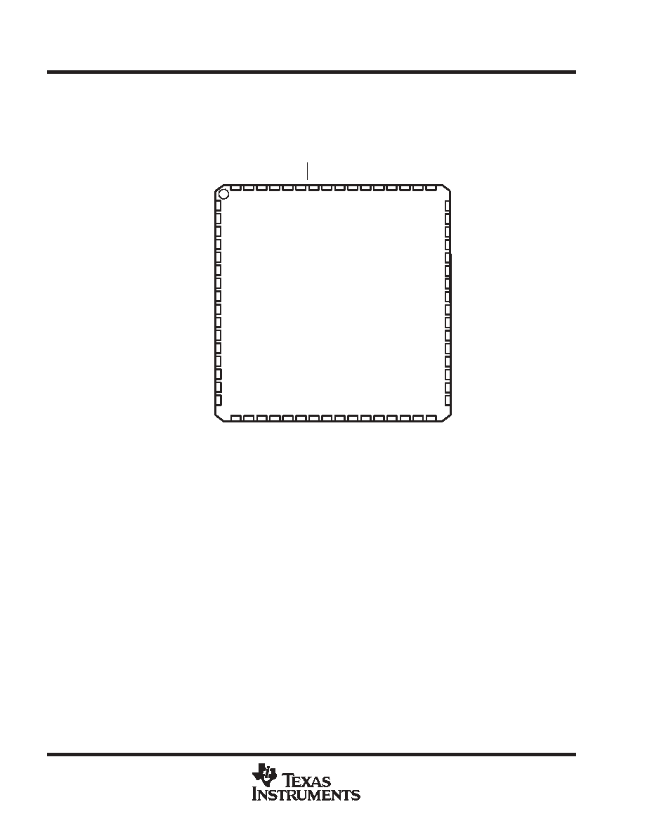
pin designation, MSP430x412, MSP430x413
17 18 19 20 21 22 23 24 25 26 27 28 29 30 31 32
64 63 62 61 60 59 58 57 56 55 54 53 52 51 50 49
P1.5/TACLK/ACLK
P6.2
P6.1
P6.0
RST/NMI
TCK
TMS
TDI/TCLK
TDO/TDI
P1.0/T
A0
P1.1/T
A0/MCLK
P1.2/T
A1
P1.3/SVSOUT
P1.4
P4.4/S5
P4.3/S6
P4.2/S7
P4.1/S8
P4.0/S9
P3.7/S10
P3.6/S1
1
P3.5/S12
P3.4/S13
P3.3/S14
P3.2/S15
P3.1/S16
P3.0/S17
P2.7/S18
P2.6/CAOUT/S19
P2.5/S20
48
47
46
45
44
43
42
41
40
39
38
37
36
35
34
33
P1.6/CA0
P1.7/CA1
P2.0/TA2
P2.1
P5.7/R33
P5.6/R23
P5.5/R13
R03
P5.4/COM3
P5.3/COM2
P5.2/COM1
COM0
P2.2/S23
P2.4/S21
P2.3/S22
1
2
3
4
5
6
7
8
9
10
11
12
13
14
15
16
P6.3
P6.4
P6.5
P6.6
P6.7
NC
XIN
XOUT
NC
NC
P5.1/S0
P5.0/S1
P4.7/S2
P4.5/S4
P4.6/S3
MSP430x412
NC - No internal connection. External connection to VSS recommended.
MSP430x413
DV
CC
AV
SS
AV
CC
DV
SS
MSP430x41x
MIXED SIGNAL MICROCONTROLLER
SLAS340G - MAY 2001 - REVISED JUNE 2004
3
POST OFFICE BOX 655303
∑
DALLAS, TEXAS 75265
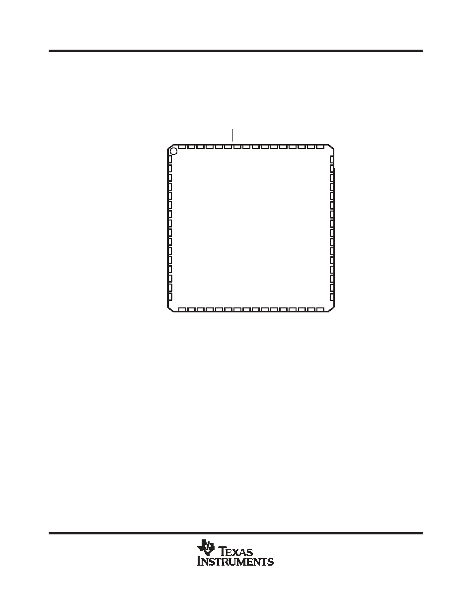
pin designation, MSP430x415, MSP430x417
17 18 19 20 21 22 23 24 25 26 27 28 29 30 31 32
64 63 62 61 60 59 58 57 56 55 54 53 52 51 50 49
P1.5/TA0CLK/ACLK
P6.2
P6.1
P6.0
RST/NMI
TCK
TMS
TDI/TCLK
TDO/TDI
P1.0/T
A0.0
P1.1/T
A0.0/MCLK
P1.2/T
A0.1
P1.3/T
A1.0/SVSOUT
P1.4/T
A1.0
P4.4/S5
P4.3/S6
P4.2/S7
P4.1/S8
P4.0/S9
P3.7/S10
P3.6/S1
1
P3.5/S12
P3.4/S13
P3.3/S14
P3.2/S15
P3.1/S16
P3.0/S17
P2.7/S18
P2.6/CAOUT/S19
P2.5/T
A1CLK/S20
48
47
46
45
44
43
42
41
40
39
38
37
36
35
34
33
P1.6/CA0
P1.7/CA1
P2.0/TA0.2
P2.1/TA1.1
P5.7/R33
P5.6/R23
P5.5/R13
R03
P5.4/COM3
P5.3/COM2
P5.2/COM1
COM0
P2.2/TA1.2/S23
P2.4/TA1.4/S21
P2.3/TA1.3/S22
1
2
3
4
5
6
7
8
9
10
11
12
13
14
15
16
P6.3
P6.4
P6.5
P6.6
P6.7
NC
XIN
XOUT
NC
P5.1/S0
P5.0/S1
P4.7/S2
P4.5/S4
P4.6/S3
MSP430x415
NC - No internal connection. External connection to VSS recommended.
MSP430x417
AV
SS2
DV
CC
AV
SS1
AV
CC
DV
SS
MSP430x41x
MIXED SIGNAL MICROCONTROLLER
SLAS340G - MAY 2001 - REVISED JUNE 2004
4
POST OFFICE BOX 655303
∑
DALLAS, TEXAS 75265
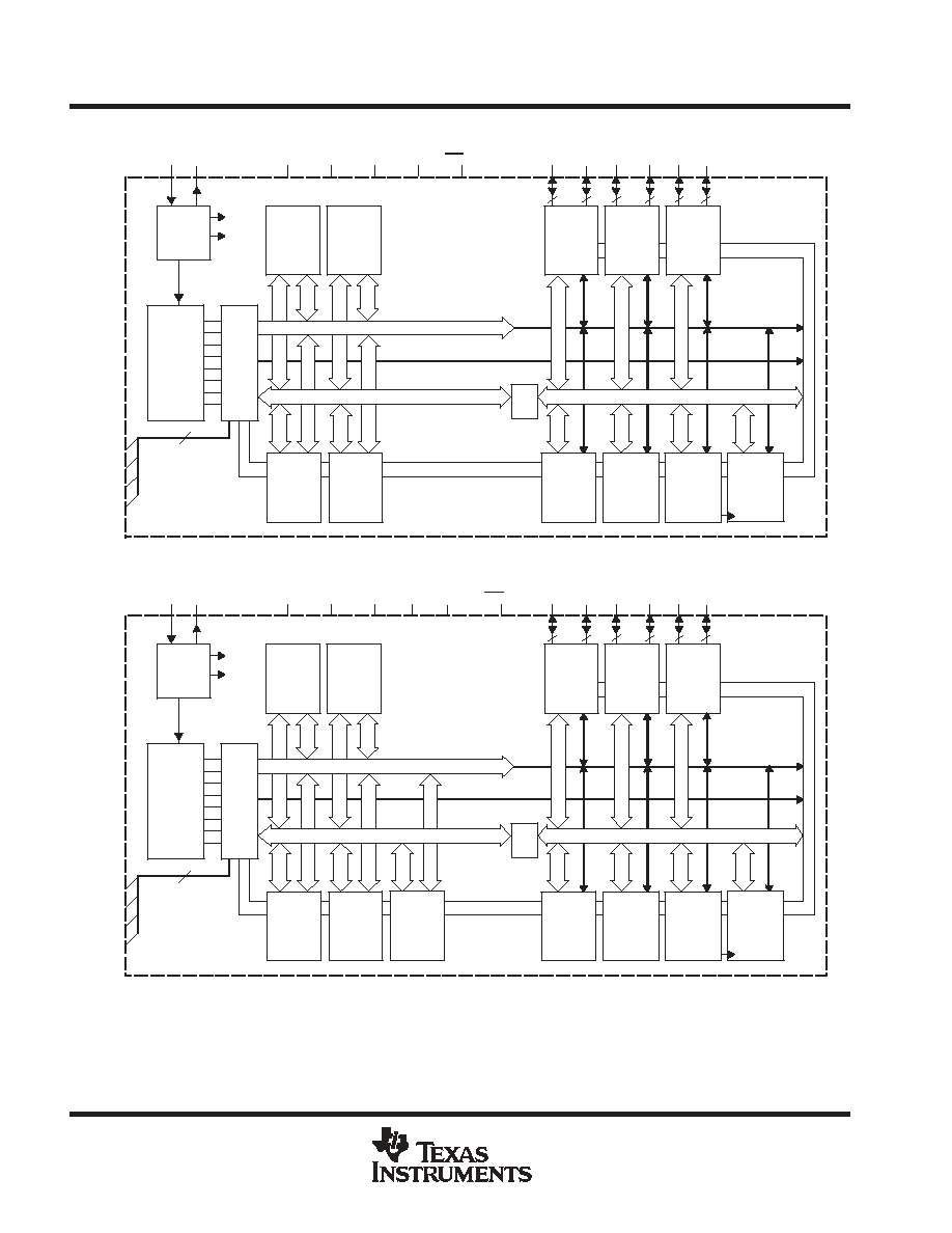
functional block diagram, MSP430x412, MSP430x413
Oscillator
ACLK
SMCLK
CPU
Incl. 16 Reg.
Bus
Conv
MCB
XIN
XOUT
P3
P4
P2
TMS
TCK
MDB, 16 Bit
MAB, 16 Bit
MCLK
4
TDI/TCLK
TDO/TDI
P5
P6
MAB,
4 Bit
DVCC
DVSS
AVCC
AVSS RST/NMI
P1
4KB/8KB
Flash-F41x
ROM-C41x
256B RAM
Watchdog
Timer
15/16-Bit
Timer_A3
3 CC Reg
Test
JTAG
Emulation
Module
I/O Port 1/2
16 I/Os,
with
Interrupt
Capability
I/O Port 3/4
16 I/Os
POR/
SVS/
Brownout
Comparator
A
Basic
Timer 1
1 Interrupt
Vector
I/O Port 5/6
16 I/Os
MDB, 8 Bit
MDB, 16-Bit
MAB, 16-Bit
LCD
96
Segments
1,2,3,4 MUX
fLCD
FLL+
8
8
8
8
8
8
functional block diagram, MSP430x415, MSP430x417
Oscillator
ACLK
SMCLK
CPU
Incl. 16 Reg.
Bus
Conv
MCB
XIN
XOUT
P3
P4
P2
TMS
TCK
MDB, 16 Bit
MAB, 16 Bit
MCLK
4
TDI/TCLK
TDO/TDI
P5
P6
MAB,
4 Bit
DVCC
DVSS
AVCC AVSS1
RST/NMI
P1
16KB Flash
32KB Flash
512B RAM
1KB RAM
Watchdog
Timer
15/16-Bit
Timer0_A3
3 CC Reg
Test
JTAG
Emulation
Module
I/O Port 1/2
16 I/Os,
with
Interrupt
Capability
I/O Port 3/4
16 I/Os
POR/
Multilevel
SVS/
Brownout
Comparator
A
Basic
Timer 1
1 Interrupt
Vector
I/O Port 5/6
16 I/Os
MDB, 8 Bit
MAB, 16-Bit
LCD
96
Segments
1,2,3,4 MUX
fLCD
FLL+
8
8
8
8
8
8
Timer1_A5
5 CC Reg
AVSS2
MDB, 16-Bit
MSP430x41x
MIXED SIGNAL MICROCONTROLLER
SLAS340G - MAY 2001 - REVISED JUNE 2004
5
POST OFFICE BOX 655303
∑
DALLAS, TEXAS 75265
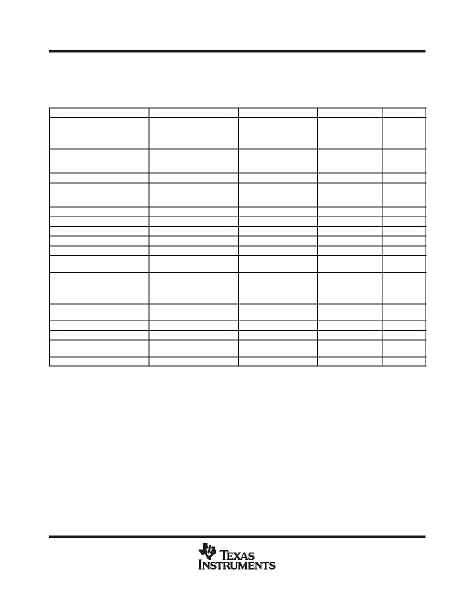
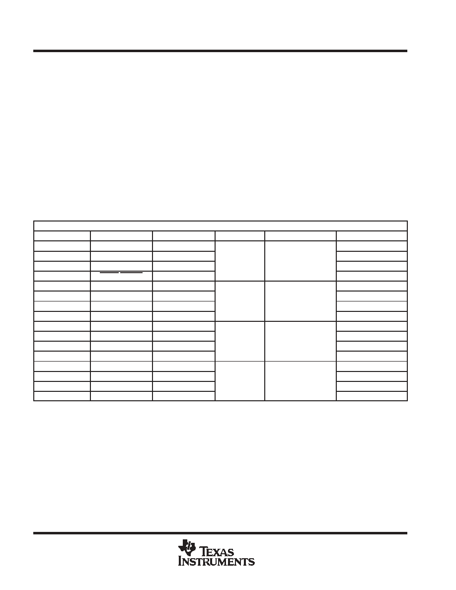
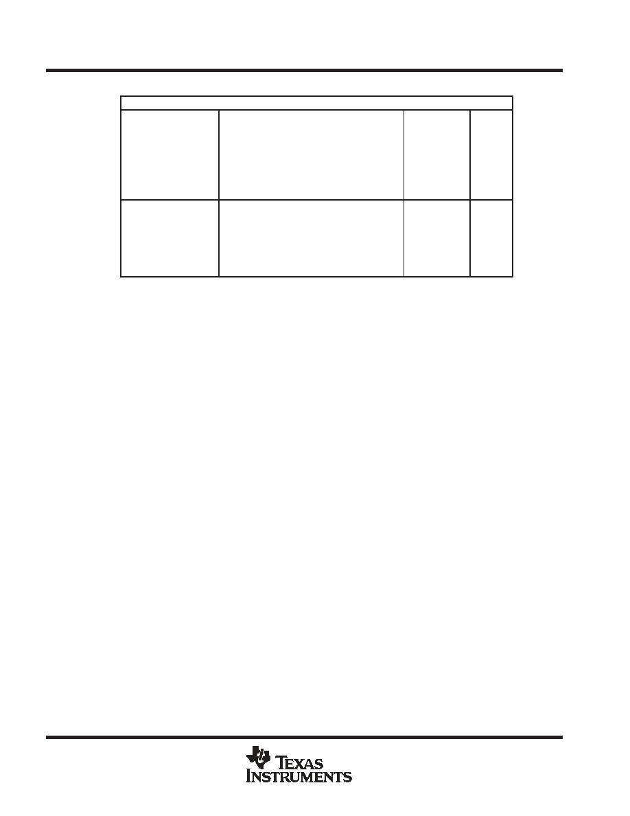
Terminal Functions
MSP430x412, MSP430x413
TERMINAL
I/O
DESCRIPTION
NAME
NO.
I/O
DESCRIPTION
AVCC
64
Positive terminal that supplies SVS, brownout, oscillator, FLL+, comparator_A, port 1, and LCD
resistive divider circuitry; must not power up prior to DVCC.
AVSS
62
Negative terminal that supplies SVS, brownout, oscillator, FLL+, comparator_A. Needs to be externally
connected to DVSS.
DVCC
1
Digital supply voltage, positive terminal. Supplies all parts, except those which are supplied via AVCC.
DVSS
63
Digital supply voltage, negative terminal. Supplies all digital parts, except those which are supplied via
AVCC/AVSS.
NC
7, 10, 11
Not internally connected. Connection to VSS recommended.
P1.0/TA0
53
I/O
General-purpose digital I/O/Timer_A. Capture: CCI0A input, compare: Out0 output/BSL transmit
P1.1/TA0/MCLK
52
I/O
General-purpose digital I/O/Timer_A. Capture: CCI0B input/MCLK output. Note: TA0 is only an input
on this pin/BSL receive
P1.2/TA1
51
I/O
General-purpose digital I/O/Timer_A, capture: CCI1A input, compare: Out1 output
P1.3/SVSOUT
50
I/O
General-purpose digital I/O/SVS: output of SVS comparator
P1.4
49
I/O
General-purpose digital I/O
P1.5/TACLK/ ACLK
48
I/O
General-purpose digital I/O/input of Timer_A clock/output of ACLK
P1.6/CA0
47
I/O
General-purpose digital I/O/Comparator_A input
P1.7/CA1
46
I/O
General-purpose digital I/O/Comparator_A input
P2.0/TA2
45
I/O
General-purpose digital I/O/ Timer_A capture: CCI2A input, compare: Out2 output
P2.1
44
I/O
General-purpose digital I/O
P2.2/S23
35
I/O
General-purpose digital I/O/LCD segment output 23 (see Note 1)
P2.3/S22
34
I/O
General-purpose digital I/O/LCD segment output 22 (see Note 1)
P2.4/S21
33
I/O
General-purpose digital I/O/LCD segment output 21 (see Note 1)
P2.5/S20
32
I/O
General-purpose digital I/O/LCD segment output 20 (see Note 1)
P2.6/CAOUT/S19
31
I/O
General-purpose digital I/O/Comparator_A output/LCD segment output 19 (see Note 1)
P2.7/S18
30
I/O
General-purpose digital I/O/LCD segment output 18 (see Note 1)
P3.0/S17
29
I/O
General-purpose digital I/O/ LCD segment output 17 (see Note 1)
P3.1/S16
28
I/O
General-purpose digital I/O/ LCD segment output 16 (see Note 1)
P3.2/S15
27
I/O
General-purpose digital I/O/ LCD segment output 15 (see Note 1)
P3.3/S14
26
I/O
General-purpose digital I/O/ LCD segment output 14 (see Note 1)
P3.4/S13
25
I/O
General-purpose digital I/O/LCD segment output 13 (see Note 1)
P3.5/S12
24
I/O
General-purpose digital I/O/LCD segment output 12 (see Note 1)
P3.6/S11
23
I/O
General-purpose digital I/O/LCD segment output 11 (see Note 1)
P3.7/S10
22
I/O
General-purpose digital I/O/LCD segment output 10 (see Note 1)
NOTE 1: LCD function selected automatically when applicable LCD module control bits are set, not with PxSEL bits.

MSP430x41x
MIXED SIGNAL MICROCONTROLLER
SLAS340G - MAY 2001 - REVISED JUNE 2004
6
POST OFFICE BOX 655303
∑
DALLAS, TEXAS 75265
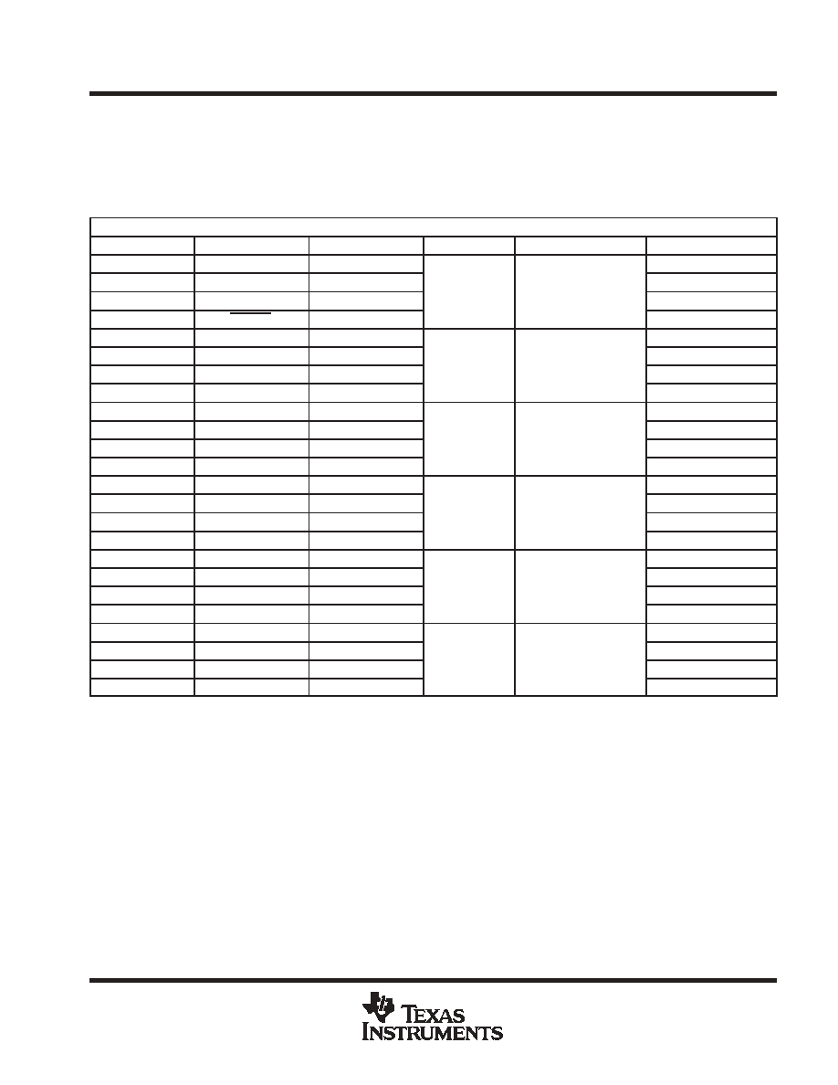
Terminal Functions (Continued)
MSP430x412, MSP430x413 (continued)
TERMINAL
I/O
DESCRIPTION
NAME
NO.
I/O
DESCRIPTION
P4.0/S9
21
I/O
General-purpose digital I/O/LCD segment output 9 (see Note 1)
P4.1/S8
20
I/O
General-purpose digital I/O/LCD segment output 8 (see Note 1)
P4.2/S7
19
I/O
General-purpose digital I/O/LCD segment output 7 (see Note 1)
P4.3/S6
18
I/O
General-purpose digital I/O/LCD segment output 6 (see Note 1)
P4.4/S5
17
I/O
General-purpose digital I/O/LCD segment output 5 (see Note 1)
P4.5/S4
16
I/O
General-purpose digital I/O/LCD segment output 4 (see Note 1)
P4.6/S3
15
I/O
General-purpose digital I/O/LCD segment output 3 (see Note 1)
P4.7/S2
14
I/O
General-purpose digital I/O/LCD segment output 2 (see Note 1)
P5.0/S1
13
I/O
General-purpose digital I/O/LCD segment output 1 (see Note 1)
P5.1/S0
12
I/O
General-purpose digital I/O/LCD segment output 0 (see Note 1)
COM0
36
O
Common output. COM0-3 are used for LCD backplanes
P5.2/COM1
37
I/O
General-purpose digital I/O/common output. COM0-3 are used for LCD backplanes
P5.3/COM2
38
I/O
General-purpose digital I/O/common output. COM0-3 are used for LCD backplanes
P5.4/COM3
39
I/O
General-purpose digital I/O/common output. COM0-3 are used for LCD backplanes
R03
40
I
Input port of fourth positive (lowest) analog LCD level (V5)
P5.5/R13
41
I/O
General-purpose digital I/O/input port of third most positive analog LCD level (V4 or V3)
P5.6/R23
42
I/O
General-purpose digital I/O/input port of second most positive analog LCD level (V2)
P5.7/R33
43
I/O
General-purpose digital I/O/output port of most positive analog LCD level (V1)
P6.0
59
I/O
General-purpose digital I/O
P6.1
60
I/O
General-purpose digital I/O
P6.2
61
I/O
General-purpose digital I/O
P6.3
2
I/O
General-purpose digital I/O
P6.4
3
I/O
General-purpose digital I/O
P6.5
4
I/O
General-purpose digital I/O
P6.6
5
I/O
General-purpose digital I/O
P6.7
6
I/O
General-purpose digital I/O
RST/NMI
58
I
Reset input or nonmaskable interrupt input port
TCK
57
I
Test clock. TCK is the clock input port for device programming and test.
TDI/TCLK
55
I
Test data input or test clock input. The device protection fuse is connected to TDI.
TDO/TDI
54
I/O
Test data output port. TDO/TDI data output or programming data input terminal.
TMS
56
I
Test mode select. TMS is used as an input port for device programming and test.
XIN
8
I
Input port for crystal oscillator XT1. Standard or watch crystals can be connected.
XOUT
9
O
Output terminal of crystal oscillator XT1.
QFN Pad
NA
NA
QFN package pad connection to VSS recommended.
NOTE 1: LCD function selected automatically when applicable LCD module control bits are set, not with PxSEL bits.
MSP430x41x
MIXED SIGNAL MICROCONTROLLER
SLAS340G - MAY 2001 - REVISED JUNE 2004
7
POST OFFICE BOX 655303
∑
DALLAS, TEXAS 75265
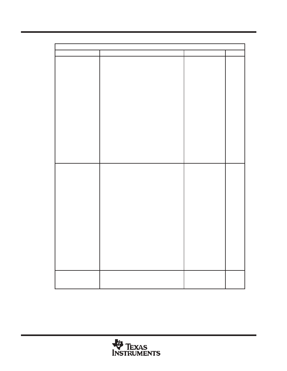
Terminal Functions (Continued)
MSP430x415, MSP430x417
TERMINAL
I/O
DESCRIPTION
NAME
NO.
I/O
DESCRIPTION
AVCC
64
Positive terminal that supplies SVS, brownout, oscillator, FLL+, comparator_A, port 1, and LCD
resistive divider circuitry; must not power up prior to DVCC.
AVSS1
62
Negative terminal that supplies SVS, brownout, oscillator, FLL+, comparator_A. Needs to be externally
connected to DVSS.
DVCC
1
Digital supply voltage, positive terminal. Supplies all parts, except those which are supplied via AVCC.
DVSS
63
Digital supply voltage, negative terminal. Supplies all digital parts, except those which are supplied via
AVCC/AVSS.
AVSS2
10
Negative terminal that supplies SVS, brownout, oscillator, FLL+, comparator_A. Needs to be externally
connected to DVSS.
NC
7, 11
Not internally connected. Connection to VSS recommended.
P1.0/TA0.0
53
I/O
General-purpose digital I/O/Timer0_A. Capture: CCI0A input, compare: Out0 output/BSL transmit
P1.1/TA0.0/MCLK
52
I/O
General-purpose digital I/O/Timer0_A. Capture: CCI0B input/MCLK output. Note: TA0 is only an input
on this pin/BSL receive
P1.2/TA0.1
51
I/O
General-purpose digital I/O/Timer0_A, capture: CCI1A input, compare: Out1 output
P1.3/TA1.0/
SVSOUT
50
I/O
General-purpose digital I/O/Timer1_A, capture: CCI0B input/SVS: output of SVS comparator
P1.4/TA1.0
49
I/O
General-purpose digital I/O/Timer1_A, capture: CCI0A input, compare: Out0 output
P1.5/TA0CLK/
ACLK
48
I/O
General-purpose digital I/O/input of Timer0_A clock/output of ACLK
P1.6/CA0
47
I/O
General-purpose digital I/O/Comparator_A input
P1.7/CA1
46
I/O
General-purpose digital I/O/Comparator_A input
P2.0/TA0.2
45
I/O
General-purpose digital I/O/ Timer0_A capture: CCI2A input, compare: Out2 output
P2.1/TA1.1
44
I/O
General-purpose digital I/O/Timer1_A, capture: CCI1A input, compare: Out1 output
P2.2/TA1.2/S23
35
I/O
General-purpose digital I/O/Timer1_A, capture: CCI2A input, compare: Out2 output/LCD segment
output 23 (see Note 1)
P2.3/TA1.3/S22
34
I/O
General-purpose digital I/O/Timer1_A, capture: CCI3A input, compare: Out3 output/LCD segment
output 22 (see Note 1)
P2.4/TA1.4/S21
33
I/O
General-purpose digital I/O/Timer1_A, capture: CCI4A input, compare: Out4 output/LCD segment
output 21 (see Note 1)
P2.5/TA1CLK/S20
32
I/O
General-purpose digital I/O/input of Timer1_A clock/LCD segment output 20 (see Note 1)
P2.6/CAOUT/S19
31
I/O
General-purpose digital I/O/Comparator_A output/LCD segment output 19 (see Note 1)
P2.7/S18
30
I/O
General-purpose digital I/O/LCD segment output 18 (see Note 1)
P3.0/S17
29
I/O
General-purpose digital I/O/ LCD segment output 17 (see Note 1)
P3.1/S16
28
I/O
General-purpose digital I/O/ LCD segment output 16 (see Note 1)
P3.2/S15
27
I/O
General-purpose digital I/O/ LCD segment output 15 (see Note 1)
P3.3/S14
26
I/O
General-purpose digital I/O/ LCD segment output 14 (see Note 1)
P3.4/S13
25
I/O
General-purpose digital I/O/LCD segment output 13 (see Note 1)
P3.5/S12
24
I/O
General-purpose digital I/O/LCD segment output 12 (see Note 1)
P3.6/S11
23
I/O
General-purpose digital I/O/LCD segment output 11 (see Note 1)
P3.7/S10
22
I/O
General-purpose digital I/O/LCD segment output 10 (see Note 1)
NOTE 1: LCD function selected automatically when applicable LCD module control bits are set, not with PxSEL bits.
MSP430x41x
MIXED SIGNAL MICROCONTROLLER
SLAS340G - MAY 2001 - REVISED JUNE 2004
8
POST OFFICE BOX 655303
∑
DALLAS, TEXAS 75265
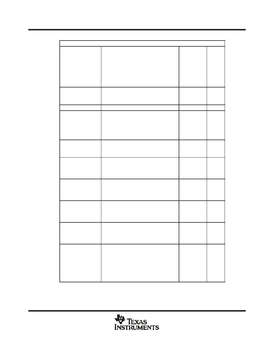
Terminal Functions (Continued)
MSP430x415, MSP430x417 (continued)
TERMINAL
I/O
DESCRIPTION
NAME
NO.
I/O
DESCRIPTION
P4.0/S9
21
I/O
General-purpose digital I/O/LCD segment output 9 (see Note 1)
P4.1/S8
20
I/O
General-purpose digital I/O/LCD segment output 8 (see Note 1)
P4.2/S7
19
I/O
General-purpose digital I/O/LCD segment output 7 (see Note 1)
P4.3/S6
18
I/O
General-purpose digital I/O/LCD segment output 6 (see Note 1)
P4.4/S5
17
I/O
General-purpose digital I/O/LCD segment output 5 (see Note 1)
P4.5/S4
16
I/O
General-purpose digital I/O/LCD segment output 4 (see Note 1)
P4.6/S3
15
I/O
General-purpose digital I/O/LCD segment output 3 (see Note 1)
P4.7/S2
14
I/O
General-purpose digital I/O/LCD segment output 2 (see Note 1)
P5.0/S1
13
I/O
General-purpose digital I/O/LCD segment output 1 (see Note 1)
P5.1/S0
12
I/O
General-purpose digital I/O/LCD segment output 0 (see Note 1)
COM0
36
O
Common output. COM0-3 are used for LCD backplanes
P5.2/COM1
37
I/O
General-purpose digital I/O/common output. COM0-3 are used for LCD backplanes
P5.3/COM2
38
I/O
General-purpose digital I/O/common output. COM0-3 are used for LCD backplanes
P5.4/COM3
39
I/O
General-purpose digital I/O/common output. COM0-3 are used for LCD backplanes
R03
40
I
Input port of fourth positive (lowest) analog LCD level (V5)
P5.5/R13
41
I/O
General-purpose digital I/O/input port of third most positive analog LCD level (V4 or V3)
P5.6/R23
42
I/O
General-purpose digital I/O/input port of second most positive analog LCD level (V2)
P5.7/R33
43
I/O
General-purpose digital I/O/output port of most positive analog LCD level (V1)
P6.0
59
I/O
General-purpose digital I/O
P6.1
60
I/O
General-purpose digital I/O
P6.2
61
I/O
General-purpose digital I/O
P6.3
2
I/O
General-purpose digital I/O
P6.4
3
I/O
General-purpose digital I/O
P6.5
4
I/O
General-purpose digital I/O
P6.6
5
I/O
General-purpose digital I/O
P6.7/SVSIN
6
I/O
General-purpose digital I/O/SVS, analog input
RST/NMI
58
I
Reset input or nonmaskable interrupt input port
TCK
57
I
Test clock. TCK is the clock input port for device programming and test.
TDI/TCLK
55
I
Test data input or test clock input. The device protection fuse is connected to TDI.
TDO/TDI
54
I/O
Test data output port. TDO/TDI data output or programming data input terminal.
TMS
56
I
Test mode select. TMS is used as an input port for device programming and test.
XIN
8
I
Input port for crystal oscillator XT1. Standard or watch crystals can be connected.
XOUT
9
O
Output terminal of crystal oscillator XT1.
QFN Pad
NA
NA
QFN package pad connection to VSS recommended.
NOTE 1: LCD function selected automatically when applicable LCD module control bits are set, not with PxSEL bits.
General-Purpose Register
Program Counter
Stack Pointer
Status Register
Constant Generator
General-Purpose Register
General-Purpose Register
General-Purpose Register
PC/R0
SP/R1
SR/CG1/R2
CG2/R3
R4
R5
R12
R13
General-Purpose Register
General-Purpose Register
R6
R7
General-Purpose Register
General-Purpose Register
R8
R9
General-Purpose Register
General-Purpose Register
R10
R11
General-Purpose Register
General-Purpose Register
R14
R15
MSP430x41x
MIXED SIGNAL MICROCONTROLLER
SLAS340G - MAY 2001 - REVISED JUNE 2004
9
POST OFFICE BOX 655303
∑
DALLAS, TEXAS 75265
short-form description
CPU
The MSP430 CPU has a 16-bit RISC architecture
that is highly transparent to the application. All
operations, other than program-flow instructions,
are performed as register operations in
conjunction with seven addressing modes for
source operand and four addressing modes for
destination operand.
The CPU is integrated with 16 registers that
provide reduced instruction execution time. The
register-to-register operation execution time is
one cycle of the CPU clock.
Four of the registers, R0 to R3, are dedicated as
program counter, stack pointer, status register,
and constant generator respectively. The
remaining registers are general-purpose
registers.
Peripherals are connected to the CPU using data,
address, and control buses, and can be handled
with all instructions.
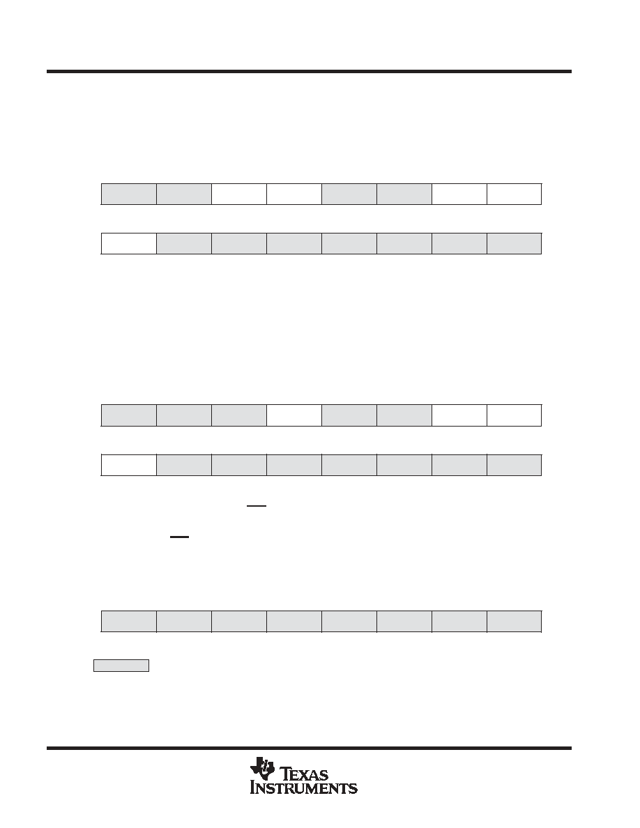
instruction set
The instruction set consists of 51 instructions with
three formats and seven address modes. Each
instruction can operate on word and byte data.
Table 1 shows examples of the three types of
instruction formats; the address modes are listed
in Table 2.
Table 1. Instruction Word Formats
Dual operands, source-destination
e.g. ADD R4,R5
R4 + R5 ---> R5
Single operands, destination only
e.g. CALL R8
PC -->(TOS), R8--> PC
Relative jump, un/conditional
e.g. JNE
Jump-on-equal bit = 0
Table 2. Address Mode Descriptions
ADDRESS MODE
S
D
SYNTAX
EXAMPLE
OPERATION
Register
D D
MOV Rs,Rd
MOV R10,R11
R10 --> R11
Indexed
D D
MOV X(Rn),Y(Rm)
MOV 2(R5),6(R6)
M(2+R5)--> M(6+R6)
Symbolic (PC relative)
D D
MOV EDE,TONI
M(EDE) --> M(TONI)
Absolute
D D
MOV &MEM,&TCDAT
M(MEM) --> M(TCDAT)
Indirect
D
MOV @Rn,Y(Rm)
MOV @R10,Tab(R6)
M(R10) --> M(Tab+R6)
Indirect
autoincrement
D
MOV @Rn+,Rm
MOV @R10+,R11
M(R10) --> R11
R10 + 2--> R10
Immediate
D
MOV #X,TONI
MOV #45,TONI
#45 --> M(TONI)
NOTE: S = source D = destination

MSP430x41x
MIXED SIGNAL MICROCONTROLLER
SLAS340G - MAY 2001 - REVISED JUNE 2004
10
POST OFFICE BOX 655303
∑
DALLAS, TEXAS 75265
operating modes
The MSP430 has one active mode and five software selectable low-power modes of operation. An interrupt
event can wake up the device from any of the five low-power modes, service the request and restore back to
the low-power mode on return from the interrupt program.
The following six operating modes can be configured by software:
D
Active mode AM;
-
All clocks are active
D
Low-power mode 0 (LPM0);
-
CPU is disabled
ACLK and SMCLK remain active, MCLK is available to modules
FLL+ Loop control remains active
D
Low-power mode 1 (LPM1);
-
CPU is disabled
ACLK and SMCLK remain active, MCLK is available to modules
FLL+ Loop control is disabled
D
Low-power mode 2 (LPM2);
-
CPU is disabled
MCLK and FLL+ loop control and DCOCLK are disabled
DCO's dc-generator remains enabled
ACLK remains active
D
Low-power mode 3 (LPM3);
-
CPU is disabled
MCLK, FLL+ loop control, and DCOCLK are disabled
DCO's dc-generator is disabled
ACLK remains active
D
Low-power mode 4 (LPM4);
-
CPU is disabled
ACLK is disabled
MCLK, FLL+ loop control, and DCOCLK are disabled
DCO's dc-generator is disabled
Crystal oscillator is stopped
MSP430x41x
MIXED SIGNAL MICROCONTROLLER
SLAS340G - MAY 2001 - REVISED JUNE 2004
11
POST OFFICE BOX 655303
∑
DALLAS, TEXAS 75265
interrupt vector addresses
The interrupt vectors and the power-up starting address are located in the ROM with an address range
0FFFFh - 0FFE0h. The vector contains the 16-bit address of the appropriate interrupt-handler instruction
sequence.
INTERRUPT SOURCE
INTERRUPT FLAG
SYSTEM INTERRUPT
WORD ADDRESS
PRIORITY
Power-up
External Reset
Watchdog
Flash memory
WDTIFG
KEYV
(see Note 1)
Reset
0FFFEh
15, highest
NMI
Oscillator Fault
Flash memory access violation
NMIIFG (see Notes 1 and 3)
OFIFG (see Notes 1 and 3)
ACCVIFG (see Notes 1 and 3)
(Non)maskable
(Non)maskable
(Non)maskable
0FFFCh
14
Timer1_A5 (see Note 4)
TA1CCR0 CCIFG (see Note 2)
Maskable
0FFFAh
13
Timer1_A5 (see Note 4)
TA1CCR1 to TA1CCR4
CCIFGs and TA1CTL TAIFG
(see Notes 1 and 2)
Maskable
0FFF8h
12
Comparator_A
CMPAIFG
Maskable
0FFF6h
11
Watchdog Timer
WDTIFG
Maskable
0FFF4h
10
0FFF2h
9
0FFF0h
8
0FFEEh
7
Timer_A3/Timer0_A3
TACCR0/TA0CCR0 CCIFG
(see Note 2)
Maskable
0FFECh
6
Timer_A3/Timer0_A3
TACCR1/TA0CCR1 and
TACCR2/TA0CCR2 CCIFGs,
and TACLT/TA0CTL TAIFG
(see Notes 1 and 2)
Maskable
0FFEAh
5
I/O port P1 (eight flags)
P1IFG.0 to P1IFG.7
(see Notes 1 and 2)
Maskable
0FFE8h
4
0FFE6h
3
0FFE4h
2
I/O port P2 (eight flags)
P2IFG.0 to P2IFG.7
(see Notes 1 and 2)
Maskable
0FFE2h
1
Basic Timer1
BTIFG
Maskable
0FFE0h
0, lowest
NOTES:
1. Multiple source flags
2. Interrupt flags are located in the module.
3. (Non)maskable: the individual interrupt-enable bit can disable an interrupt event, but the general interrupt-enable cannot.
4. Implemented in MSP430x415 and MSP430x417 devices only.
MSP430x41x
MIXED SIGNAL MICROCONTROLLER
SLAS340G - MAY 2001 - REVISED JUNE 2004
12
POST OFFICE BOX 655303
∑
DALLAS, TEXAS 75265
special function registers
Most interrupt and module enable bits are collected into the lowest address space. Special function register bits
that are not allocated to a functional purpose are not physically present in the device. Simple software access
is provided with this arrangement.
interrupt enable 1 and 2
7
6
5
4
0
OFIE
WDTIE
3
2
1
rw-0
rw-0
rw-0
Address
0h
ACCVIE
NMIIE
rw-0
7
6
5
4
0
3
2
1
Address
1h
BTIE
rw-0
WDTIE:
Watchdog-timer interrupt enable. Inactive if watchdog mode is selected. Active if watchdog timer is config-
ured in interval timer mode.
OFIE:
Oscillator-fault-interrupt enable
NMIIE:
Nonmaskable-interrupt enable
ACCVIE:
Flash access violation interrupt enable
BTIE:
Basic Timer1 interrupt enable
interrupt flag register 1 and 2
7
6
5
4
0
OFIFG
WDTIFG
3
2
1
rw-0
rw-1
rw-(0)
Address
02h
NMIIFG
7
6
5
4
0
3
2
1
Address
3h
BTIFG
rw-0
WDTIFG:
Set on watchdog-timer overflow (in watchdog mode) or security key violation. Reset with V
CC
power-up,
or a reset condition at the RST/NMI pin in reset mode.
OFIFG:
Flag set on oscillator fault
NMIIFG:
Set via RST/NMI pin
BTIFG:
Basic Timer1 interrupt flag
module enable registers 1 and 2
7
6
5
4
0
3
2
1
Address
04h/05h
rw-0:
Legend: rw:
Bit Can Be Read and Written
Bit Can Be Read and Written. It Is Reset by PUC.
SFR Bit Not Present in Device
MSP430x41x
MIXED SIGNAL MICROCONTROLLER
SLAS340G - MAY 2001 - REVISED JUNE 2004
13
POST OFFICE BOX 655303
∑
DALLAS, TEXAS 75265
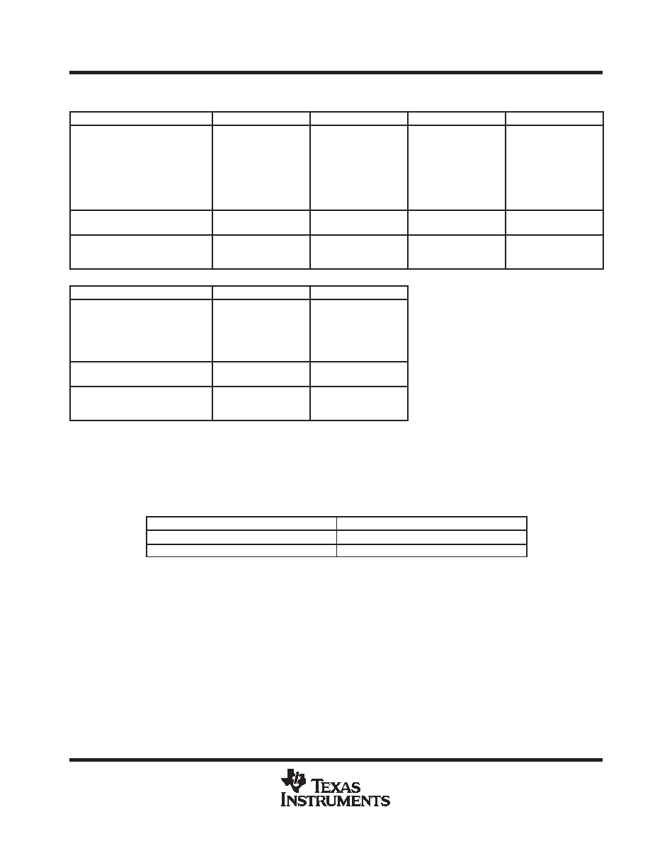
memory organization
MSP430F412
MSP430F413
MSP430F415
MSP430F417
Memory
Interrupt vector
Code memory
Size
Flash
Flash
4KB
0FFFFh - 0FFE0h
0FFFFh - 0F000h
8KB
0FFFFh - 0FFE0h
0FFFFh - 0E000h
16KB
0FFFFh - 0FFE0h
0FFFFh - 0C000h
32KB
0FFFFh - 0FFE0h
0FFFFh - 08000h
Information memory
Size
Flash
256 Byte
010FFh - 01000h
256 Byte
010FFh - 01000h
256 Byte
010FFh - 01000h
256 Byte
010FFh - 01000h
Boot memory
Size
ROM
1KB
0FFFh - 0C00h
1KB
0FFFh - 0C00h
1KB
0FFFh - 0C00h
1KB
0FFFh - 0C00h
RAM
Size
256 Byte
02FFh - 0200h
256 Byte
02FFh - 0200h
512 Byte
03FFh - 0200h
1 KB
05FFh - 0200h
Peripherals
16-bit
8-bit
8-bit SFR
01FFh - 0100h
0FFh - 010h
0Fh - 00h
01FFh - 0100h
0FFh - 010h
0Fh - 00h
01FFh - 0100h
0FFh - 010h
0Fh - 00h
01FFh - 0100h
0FFh - 010h
0Fh - 00h
MSP430C412
MSP430C413
Memory
Interrupt vector
Code memory
Size
ROM
ROM
4KB
0FFFFh - 0FFE0h
0FFFFh - 0F000h
8KB
0FFFFh - 0FFE0h
0FFFFh - 0E000h
Information memory
Size
NA
NA
Boot memory
Size
NA
NA
RAM
Size
256 Byte
02FFh - 0200h
256 Byte
02FFh - 0200h
Peripherals
16-bit
8-bit
8-bit SFR
01FFh - 0100h
0FFh - 010h
0Fh - 00h
01FFh - 0100h
0FFh - 010h
0Fh - 00h
bootstrap loader (BSL)
The MSP430 bootstrap loader (BSL) enables users to program the flash memory or RAM using a UART serial
interface. Access to the MSP430 memory via the BSL is protected by user-defined password. For complete
description of the features of the BSL and its implementation, see the Application report Features of the MSP430
Bootstrap Loader, Literature Number SLAA089.
BSL Function
PM, RTD Package Pins
Data Transmit
53 - P1.0
Data Receive
52 - P1.1
MSP430x41x
MIXED SIGNAL MICROCONTROLLER
SLAS340G - MAY 2001 - REVISED JUNE 2004
14
POST OFFICE BOX 655303
∑
DALLAS, TEXAS 75265
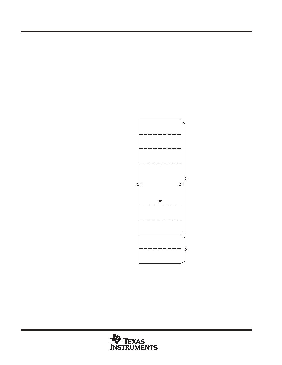
flash memory
The flash memory can be programmed via the JTAG port, the bootstrap loader, or in-system by the CPU. The
CPU can perform single-byte and single-word writes to the flash memory. Features of the flash memory include:
D
Flash memory has n segments of main memory and two segments of information memory (A and B) of 128
bytes each. Each segment in main memory is 512 bytes in size.
D
Segments 0 to n may be erased in one step, or each segment may be individually erased.
D
Segments A and B can be erased individually, or as a group with segments 0-n.
Segments A and B are also called information memory.
D
New devices may have some bytes programmed in the information memory (needed for test during
manufacturing). The user should perform an erase of the information memory prior to the first use.
Segment 0
With Interrupt Vectors
Segment 1
Segment 2
Segment n-1
Segment n
32KB
Segment A
Segment B
Main Memory
Information Memory
0FFFFh
0FA00h
0FE00h
0FDFFh
0FC00h
0FBFFh
0F9FFh
08400h
083FFh
08200h
081FFh
01000h
010FFh
08000h
01080h
0107Fh
16KB
0FFFFh
0FA00h
0FE00h
0FDFFh
0FC00h
0FBFFh
0F9FFh
0C400h
0C3FFh
0C200h
0C1FFh
01000h
010FFh
0C000h
01080h
0107Fh
8KB
0FFFFh
0FA00h
0FE00h
0FDFFh
0FC00h
0FBFFh
0F9FFh
0E400h
0E3FFh
0E200h
0E1FFh
01000h
010FFh
0E000h
01080h
0107Fh
4KB
0FFFFh
0FA00h
0FE00h
0FDFFh
0FC00h
0FBFFh
0F9FFh
0F400h
0F3FFh
0F200h
0F1FFh
01000h
010FFh
0F000h
01080h
0107Fh

MSP430x41x
MIXED SIGNAL MICROCONTROLLER
SLAS340G - MAY 2001 - REVISED JUNE 2004
15
POST OFFICE BOX 655303
∑
DALLAS, TEXAS 75265
peripherals
Peripherals are connected to the CPU through data, address, and control busses and can be handled using
all instructions. For complete module descriptions, refer to the MSP430x4xx Family User's Guide, literature
number SLAU056.
oscillator and system clock
The clock system in the MSP430x41x family of devices is supported by the FLL+ module that includes support
for a 32768-Hz watch crystal oscillator, an internal digitally-controlled oscillator (DCO) and a high frequency
crystal oscillator. The FLL+ clock module is designed to meet the requirements of both low system cost and
low-power consumption. The FLL+ features a digital frequency locked loop (FLL) hardware which in conjunction
with a digital modulator stabilizes the DCO frequency to a programmable multiple of the watch crystal frequency.
The internal DCO provides a fast turn-on clock source and stabilizes in less than 6
µ
s. The FLL+ module
provides the following clock signals:
D
Auxiliary clock (ACLK), sourced from a 32768-Hz watch crystal or a high frequency crystal.
D
Main clock (MCLK), the system clock used by the CPU.
D
Sub-Main clock (SMCLK), the sub-system clock used by the peripheral modules.
D
ACLK/n, the buffered output of ACLK, ACLK/2, ACLK/4, or ACLK/8.
brownout, supply voltage supervisor
The brownout circuit is implemented to provide the proper internal reset signal to the device during power on
and power off. The supply voltage supervisor (SVS) circuitry detects if the supply voltage drops below a fixed
level or user selectable level (MSP430x415 & MSP430x417 only) and supports both supply voltage supervision
(the device is automatically reset) and supply voltage monitoring (SVM, the device is not automatically reset).
The CPU begins code execution after the brownout circuit releases the device reset. However, V
CC
may not
have ramped to V
CC(min)
at that time. The user must insure the default FLL+ settings are not changed until V
CC
reaches V
CC(min)
. If desired, the SVS circuit can be used to determine when V
CC
reaches V
CC(min)
.
digital I/O
There are six 8-bit I/O ports implemented--ports P1 through P6:
D
All individual I/O bits are independently programmable.
D
Any combination of input, output, and interrupt conditions is possible.
D
Edge-selectable interrupt input capability for all the eight bits of ports P1 and P2.
D
Read/write access to port-control registers is supported by all instructions.
Basic Timer1
The Basic Timer1 has two independent 8-bit timers which can be cascaded to form a 16-bit timer/counter. Both
timers can be read and written by software. The Basic Timer1 can be used to generate periodic interrupts and
clock for the LCD module.
LCD drive
The LCD driver generates the segment and common signals required to drive an LCD display. The LCD
controller has dedicated data memory to hold segment drive information. Common and segment signals are
generated as defined by the mode. Static, 2-MUX, 3-MUX, and 4-MUX LCDs are supported by this peripheral.
MSP430x41x
MIXED SIGNAL MICROCONTROLLER
SLAS340G - MAY 2001 - REVISED JUNE 2004
16
POST OFFICE BOX 655303
∑
DALLAS, TEXAS 75265
watchdog timer
The primary function of the watchdog timer (WDT) module is to perform a controlled system restart after a
software problem occurs. If the selected time interval expires, a system reset is generated. If the watchdog
function is not needed in an application, the module can be configured as an interval timer and can generate
interrupts at selected time intervals.
comparator_A
The primary function of the comparator_A module is to support precision slope analog-to-digital conversions,
battery-voltage supervision, and monitoring of external analog signals.
timer_A3/timer0_A3
Timer_A3/Timer0_A3 is a 16-bit timer/counter with three capture/compare registers. Timer_A3/Timer0_A3 can
support multiple capture/compares, PWM outputs, and interval timing. Timer_A3/Timer0_A3 also has extensive
interrupt capabilities. Interrupts may be generated from the counter on overflow conditions and from each of
the capture/compare registers.
Timer_A3/Timer0_A3 Signal Connections
Input Pin Number
Device Input Signal
Module Input Name
Module Block
Module Output Signal
Output Pin Number
48 - P1.5
TACLK/TA0CLK
TACLK
ACLK
ACLK
Timer
NA
SMCLK
SMCLK
Timer
NA
48 - P1.5
TACLK/TA0CLK
INCLK
53 - P1.0
TA0/TA0.0
CCI0A
53 - P1.0
52 - P1.1
TA0/TA0.0
CCI0B
CCR0
TA0/TA0.0
DVSS
GND
CCR0
TA0/TA0.0
DVCC
VCC
51 - P1.2
TA1/TA0.1
CCI1A
51 - P1.2
CAOUT (internal)
CCI1B
CCR1
TA1/TA0.1
DVSS
GND
CCR1
TA1/TA0.1
DVCC
VCC
45 - P2.0
TA2/TA0.2
CCI2A
45 - P2.0
ACLK (internal)
CCI2B
CCR2
TA2/TA0.2
DVSS
GND
CCR2
TA2/TA0.2
DVCC
VCC
MSP430x41x
MIXED SIGNAL MICROCONTROLLER
SLAS340G - MAY 2001 - REVISED JUNE 2004
17
POST OFFICE BOX 655303
∑
DALLAS, TEXAS 75265
timer1_A5 (MSP430x415 and MSP430x417 only)
Timer1_A5 is a 16-bit timer/counter with five capture/compare registers. Timer1_A5 can support multiple
capture/compares, PWM outputs, and interval timing. Timer1_A5 also has extensive interrupt capabilities.
Interrupts may be generated from the counter on overflow conditions and from each of the capture/compare
registers.
Timer1_A5 Signal Connections
Input Pin Number
Device Input Signal
Module Input Name
Module Block
Module Output Signal
Output Pin Number
32 - P2.5
TA1CLK
TACLK
ACLK
ACLK
Timer
NA
SMCLK
SMCLK
Timer
NA
32 - P2.5
TA1CLK
INCLK
49 - P1.4
TA1.0
CCI0A
49 - P1.4
50 - P1.3
TA1.0
CCI0B
CCR0
TA1.0
DVSS
GND
CCR0
TA1.0
DVCC
VCC
44 - P2.1
TA1.1
CCI1A
44 - P2.1
CAOUT (internal)
CCI1B
CCR1
TA1.1
DVSS
GND
CCR1
TA1.1
DVCC
VCC
35 - P2.2
TA1.2
CCI2A
35 - P2.2
Not Connected
CCI2B
CCR2
TA1.2
DVSS
GND
CCR2
TA1.2
DVCC
VCC
34 - P2.3
TA1.3
CCI3A
34 - P2.3
Not Connected
CCI3B
CCR3
TA1.3
DVSS
GND
CCR3
TA1.3
DVCC
VCC
33 - P2.4
TA1.4
CCI4A
33 - P2.4
Not Connected
CCI4B
CCR4
TA1.4
DVSS
GND
CCR4
TA1.4
DVCC
VCC
MSP430x41x
MIXED SIGNAL MICROCONTROLLER
SLAS340G - MAY 2001 - REVISED JUNE 2004
18
POST OFFICE BOX 655303
∑
DALLAS, TEXAS 75265
peripheral file map
PERIPHERALS WITH WORD ACCESS
Watchdog
Watchdog Timer control
WDTCTL
0120h
Timer1_A5
(MSP430x415 and
Timer1_A interrupt vector
TA1IV
011Eh
Timer1_A5
(MSP430x415 and
MSP430x417 only)
Timer1_A control
TA1CTL
0180h
MSP430x417 only)
Capture/compare control 0
TA1CCTL0
0182h
Capture/compare control 1
TA1CCTL1
0184h
Capture/compare control 2
TA1CCTL2
0186h
Capture/compare control 3
TA1CCTL3
0188h
Capture/compare control 4
TA1CCTL4
018Ah
Reserved
018Ch
Reserved
018Eh
Timer1_A register
TA1R
0190h
Capture/compare register 0
TA1CCR0
0192h
Capture/compare register 1
TA1CCR1
0194h
Capture/compare register 2
TA1CCR2
0196h
Capture/compare register 3
TA1CCR3
0198h
Capture/compare register 4
TA1CCR4
019Ah
Reserved
019Ch
Reserved
019Eh
Timer_A3/Timer0_A3
Timer_A/Timer0_A interrupt vector
TAIV/TA0IV
012Eh
Timer_A3/Timer0_A3
Timer_A/Timer0_A control
TACTL/TA0CTL
0160h
Capture/compare control 0
TACCTL0/TA0CCTL0
0162h
Capture/compare control 1
TACCTL1/TA0CCTL1
0164h
Capture/compare control 2
TACCTL2/TA0CCTL2
0166h
Reserved
0168h
Reserved
016Ah
Reserved
016Ch
Reserved
016Eh
Timer_A/Timer0_A register
TAR/TA0R
0170h
Capture/compare register 0
TACCR0/TA0CCR0
0172h
Capture/compare register 1
TACCR1/TA0CCR1
0174h
Capture/compare register 2
TACCR2/TA0CCR2
0176h
Reserved
0178h
Reserved
017Ah
Reserved
017Ch
Reserved
017Eh
Flash
Flash control 3
FCTL3
012Ch
Flash
Flash control 2
FCTL2
012Ah
Flash control 1
FCTL1
0128h
MSP430x41x
MIXED SIGNAL MICROCONTROLLER
SLAS340G - MAY 2001 - REVISED JUNE 2004
19
POST OFFICE BOX 655303
∑
DALLAS, TEXAS 75265
peripheral file map (continued)
PERIPHERALS WITH BYTE ACCESS
LCD
LCD memory 20
LCDM20
0A4h
LCD
:
:
:
LCD memory 16
LCDM16
0A0h
LCD memory 15
LCDM15
09Fh
:
:
:
LCD memory 1
LCDM1
091h
LCD control and mode
LCDCTL
090h
Comparator_A
Comparator_A port disable
CAPD
05Bh
Comparator_A
Comparator_A control2
CACTL2
05Ah
Comparator_A control1
CACTL1
059h
Brownout, SVS
SVS control register
SVSCTL
056h
FLL+ Clock
FLL+ Control1
FLL_CTL1
054h
FLL+ Clock
FLL+ Control0
FLL_CTL0
053h
System clock frequency control
SCFQCTL
052h
System clock frequency integrator
SCFI1
051h
System clock frequency integrator
SCFI0
050h
Basic Timer1
BT counter2
BTCNT2
047h
Basic Timer1
BT counter1
BTCNT1
046h
BT control
BTCTL
040h
Port P6
Port P6 selection
P6SEL
037h
Port P6
Port P6 direction
P6DIR
036h
Port P6 output
P6OUT
035h
Port P6 input
P6IN
034h
Port P5
Port P5 selection
P5SEL
033h
Port P5
Port P5 direction
P5DIR
032h
Port P5 output
P5OUT
031h
Port P5 input
P5IN
030h
Port P4
Port P4 selection
P4SEL
01Fh
Port P4
Port P4 direction
P4DIR
01Eh
Port P4 output
P4OUT
01Dh
Port P4 input
P4IN
01Ch
Port P3
Port P3 selection
P3SEL
01Bh
Port P3
Port P3 direction
P3DIR
01Ah
Port P3 output
P3OUT
019h
Port P3 input
P3IN
018h
Port P2
Port P2 selection
P2SEL
02Eh
Port P2
Port P2 interrupt enable
P2IE
02Dh
Port P2 interrupt-edge select
P2IES
02Ch
Port P2 interrupt flag
P2IFG
02Bh
Port P2 direction
P2DIR
02Ah
Port P2 output
P2OUT
029h
Port P2 input
P2IN
028h
MSP430x41x
MIXED SIGNAL MICROCONTROLLER
SLAS340G - MAY 2001 - REVISED JUNE 2004
20
POST OFFICE BOX 655303
∑
DALLAS, TEXAS 75265
peripheral file map (continued)
PERIPHERALS WITH BYTE ACCESS (CONTINUED)
Port P1
Port P1 selection
P1SEL
026h
Port P1
Port P1 interrupt enable
P1IE
025h
Port P1 interrupt-edge select
P1IES
024h
Port P1 interrupt flag
P1IFG
023h
Port P1 direction
P1DIR
022h
Port P1 output
P1OUT
021h
Port P1 input
P1IN
020h
Special Functions
SFR module enable 2
ME2
005h
Special Functions
SFR module enable 1
ME1
004h
SFR interrupt flag2
IFG2
003h
SFR interrupt flag1
IFG1
002h
SFR interrupt enable2
IE2
001h
SFR interrupt enable1
IE1
000h
absolute maximum ratings
Voltage applied at V
CC
to V
SS
-0.3 V to + 4.1 V
. . . . . . . . . . . . . . . . . . . . . . . . . . . . . . . . . . . . . . . . . . . . . . . . . . . .
Voltage applied to any pin (see Note)
-0.3 V to V
CC
+ 0.3 V
. . . . . . . . . . . . . . . . . . . . . . . . . . . . . . . . . . . . . . . . . .
Diode current at any device terminal .
±
2 mA
. . . . . . . . . . . . . . . . . . . . . . . . . . . . . . . . . . . . . . . . . . . . . . . . . . . . . .
Storage temperature (unprogrammed device)
-55
∞
C to 150
∞
C
. . . . . . . . . . . . . . . . . . . . . . . . . . . . . . . . . . . . . . .
Storage temperature (programmed device)
-40
∞
C to 85
∞
C
. . . . . . . . . . . . . . . . . . . . . . . . . . . . . . . . . . . . . . . . . .
Stresses beyond those listed under "absolute maximum ratings" may cause permanent damage to the device. These are stress ratings only, and
functional operation of the device at these or any other conditions beyond those indicated under "recommended operating conditions" is not
implied. Exposure to absolute-maximum-rated conditions for extended periods may affect device reliability.
NOTE: All voltages referenced to VSS. The JTAG fuse-blow voltage, VFB, is allowed to exceed the absolute maximum rating. The voltage is applied
to the TDI/TCLK pin when blowing the JTAG fuse.
MSP430x41x
MIXED SIGNAL MICROCONTROLLER
SLAS340G - MAY 2001 - REVISED JUNE 2004
21
POST OFFICE BOX 655303
∑
DALLAS, TEXAS 75265
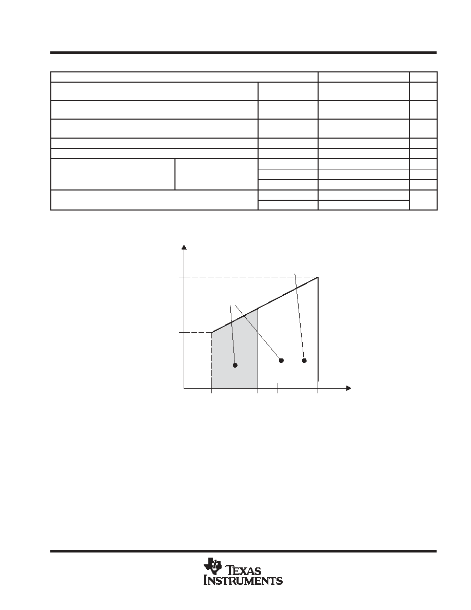
recommended operating conditions
PARAMETER
MIN
NOM
MAX
UNITS
Supply voltage during program execution, SVS disabled
VCC (AVCC = DVCC = VCC)
MSP430x41x
1.8
3.6
V
Supply voltage during program execution, SVS enabled (see Note 1),
VCC (AVCC = DVCC = VCC)
MSP430x41x
2.2
3.6
V
Supply voltage during programming of flash memory,
VCC (AVCC = DVCC = VCC)
MSP430F41x
2.7
3.6
V
Supply voltage, VSS (AVSS/1/2 = DVSS = VSS)
0
0
V
Operating free-air temperature range, TA
MSP430x41x
-40
85
∞
C
LFXT1 crystal frequency, f(LFXT1)
LF selected, XTS_FLL=0
Watch crystal
32768
Hz
LFXT1 crystal frequency, f(LFXT1)
(see Note 2)
XT1 selected, XTS_FLL=1
Ceramic resonator
450
8000
kHz
(see Note 2)
XT1 selected, XTS_FLL=1
Crystal
1000
8000
kHz
Processor frequency (signal MCLK), f(System)
VCC = 1.8 V
DC
4.15
MHz
Processor frequency (signal MCLK), f(System)
VCC = 3.6 V
DC
8
MHz
NOTES:
1. The minimum operating supply voltage is defined according to the trip point where POR is going active by decreasing supply voltage.
POR is going inactive when the supply voltage is raised above minimum supply voltage plus the hysteresis of the SVS circuitry.
2. The LFXT1 oscillator in LF-mode requires a watch crystal.
f (MHz)
1.8 V
3.6 V
2.7 V
3 V
ŒŒŒŒŒŒ
ŒŒŒŒŒŒ
ŒŒŒŒŒŒ
ŒŒŒŒŒŒ
ŒŒŒŒŒŒ
ŒŒŒŒŒŒ
ŒŒŒŒŒŒ
ŒŒŒŒŒŒ
ŒŒŒŒŒŒ
ŒŒŒŒŒŒ
4.15 MHz
8 MHz
VCC - Supply Voltage - V
f (System)
- Maximum Processor Frequency - MHz
Supply Voltage Range, x41x
During Program Execution
Supply Voltage Range
During Programming of
the Flash Memory
Figure 1. Frequency vs Supply Voltage
MSP430x41x
MIXED SIGNAL MICROCONTROLLER
SLAS340G - MAY 2001 - REVISED JUNE 2004
22
POST OFFICE BOX 655303
∑
DALLAS, TEXAS 75265
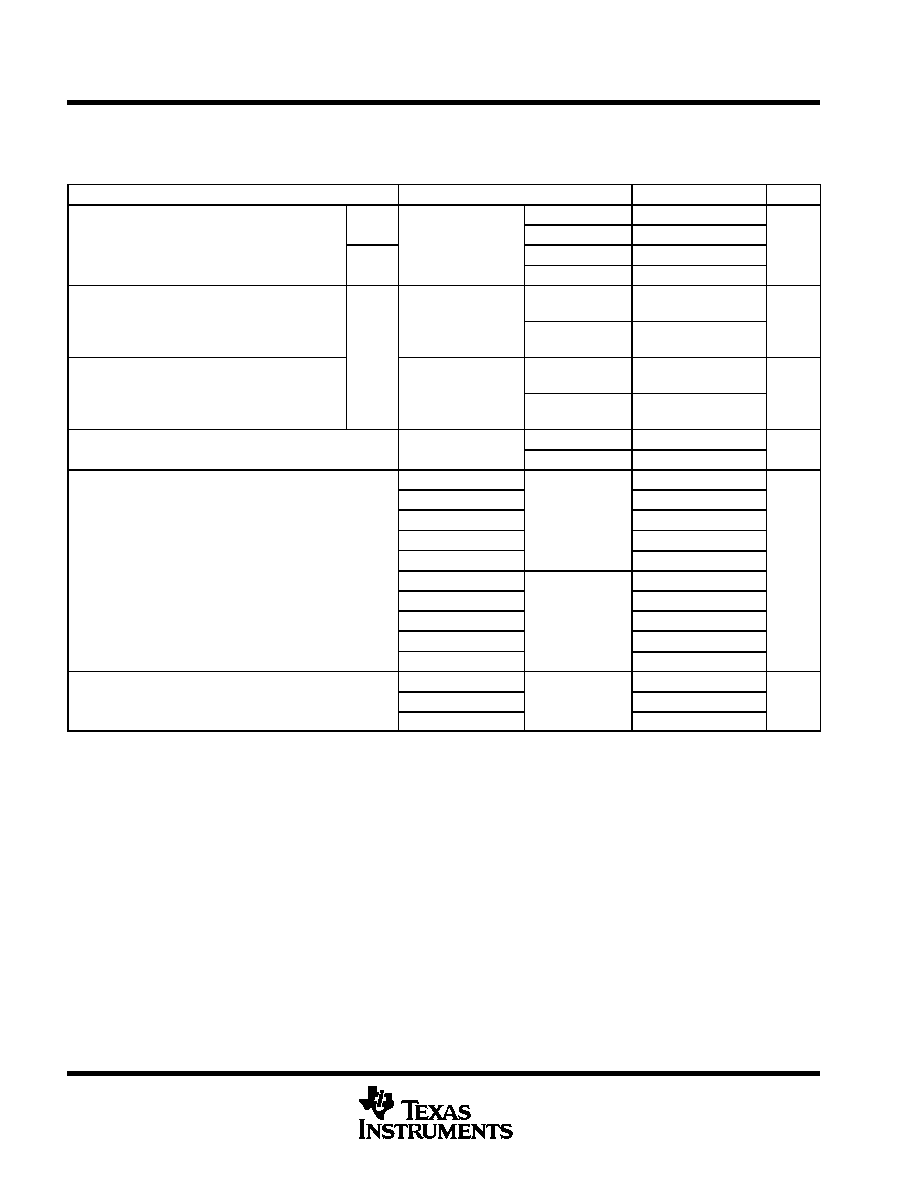
electrical characteristics over recommended operating free-air temperature (unless otherwise
noted)
supply current into AV
CC
+ DV
CC
excluding external current, (see Note 1)
PARAMETER
TEST CONDITIONS
MIN
NOM
MAX
UNIT
V
CC
= 2.2 V
160
200
Active mode,
f
(MCLK)
= f
(SMCLK)
= 1 MHz,
C41x
∞
∞
V
CC
= 3 V
240
300
I
(AM)
f
(MCLK)
= f
(SMCLK)
= 1 MHz,
f
(ACLK)
= 32,768 Hz, XTS_FLL = 0
T
A
= -40
∞
C to 85
∞
C
V
CC
= 2.2 V
200
250
µ
A
(ACLK)
(F41x: Program executes in flash)
F41x
V
CC
= 3 V
300
350
Low-power mode, (LPM0)
f
(MCLK)
= f
(SMCLK)
= 0.5 MHz,
∞
∞
V
CC
= 2.2 V
32
45
I
(LPM0)
f
(MCLK)
= f
(SMCLK)
= 0.5 MHz,
f
(ACLK)
= 32,768 Hz, XTS_FLL = 0
FN_8=FN_4=FN_3=FN_2=0
C41x
T
A
= -40
∞
C to 85
∞
C
V
CC
= 3 V
55
70
µ
A
Low-power mode, (LPM0)
f
(MCLK)
= f
(SMCLK)
= 1 MHz,
C41x
F41x
∞
∞
V
CC
= 2.2 V
57
70
I
(LPM0)
f
(MCLK)
= f
(SMCLK)
= 1 MHz,
f
(ACLK)
= 32,768 Hz, XTS_FLL = 0
FN_8=FN_4=FN_3=FN_2=0
T
A
= -40
∞
C to 85
∞
C
V
CC
= 3 V
92
100
µ
A
∞
∞
V
CC
= 2.2 V
11
14
I
(LPM2)
Low-power mode, (LPM2)
T
A
= -40
∞
C to 85
∞
C
V
CC
= 3 V
17
22
µ
A
T
A
= -40
∞
C
0.95
1.4
T
A
= -10
∞
C
0.8
1.3
T
A
= 25
∞
C
V
CC
= 2.2 V
0.7
1.2
T
A
= 60
∞
C
V
CC
= 2.2 V
0.95
1.4
T
A
= 85
∞
C
1.6
2.3
I
(LPM3)
Low-power mode, (LPM3) (see Note 2)
T
A
= -40
∞
C
1.1
1.7
µ
A
T
A
= -10
∞
C
1.0
1.6
T
A
= 25
∞
C
V
CC
= 3 V
0.9
1.5
T
A
= 60
∞
C
V
CC
= 3 V
1.1
1.7
T
A
= 85
∞
C
2.0
2.6
T
A
= -40
∞
C
0.1
0.5
I
(LPM4)
Low-power mode, (LPM4)
T
A
= 25
∞
C
V
CC
= 2.2 V/3 V
0.1
0.5
µ
A
I
(LPM4)
Low-power mode, (LPM4)
T
A
= 85
∞
C
V
CC
= 2.2 V/3 V
0.8
2.5
µ
A
NOTES:
1. All inputs are tied to 0 V or V
CC
. Outputs do not source or sink any current. The current consumption is measured with active Basic
Timer1 and LCD (ACLK selected).
The current consumption of the Comparator_A and the SVS module are specified in the respective sections.
2. The LPM3 currents are characterized with a KDS Daishinku DT-38 (6 pF) crystal.
current consumption of active mode versus system frequency, F version
I
(AM)
= I
(AM) [1 MHz]
◊
f
(System) [MHz]
current consumption of active mode versus supply voltage, F version
I
(AM)
= I
(AM) [3 V]
+ 140
µ
A/V
◊
(V
CC
≠ 3 V)
MSP430x41x
MIXED SIGNAL MICROCONTROLLER
SLAS340G - MAY 2001 - REVISED JUNE 2004
23
POST OFFICE BOX 655303
∑
DALLAS, TEXAS 75265
electrical characteristics over recommended operating free-air temperature (unless otherwise
noted) (continued)
Schmitt-trigger inputs - Ports P1, P2, P3, P4, P5, and P6
PARAMETER
VCC
MIN
TYP
MAX
UNIT
VIT+
Positive-going input threshold voltage
2.2 V
1.1
1.5
V
VIT+
Positive-going input threshold voltage
3 V
1.5
1.9
V
VIT-
Negative-going input threshold voltage
2.2 V
0.4
0.9
V
VIT-
Negative-going input threshold voltage
3 V
0.9
1.3
V
Vhys
Input voltage hysteresis (VIT+ - VIT-)
2.2 V
0.3
1.1
V
Vhys
Input voltage hysteresis (VIT+ - VIT-)
3 V
0.45
1
V
standard inputs - RST/NMI; JTAG: TCK, TMS, TDI/TCLK, TDO/TDI
PARAMETER
VCC
MIN
TYP
MAX
UNIT
VIL
Low-level input voltage
2.2 V/3 V
VSS
VSS+0.6
V
VIH
High-level input voltage
2.2 V/3 V
0.8
◊
VCC
VCC
V
inputs Px.x, TAx/TAx.x
PARAMETER
TEST CONDITIONS
VCC
MIN
TYP
MAX
UNIT
Port P1, P2: P1.x to P2.x, External
2.2 V/3 V
1.5
cycle
t(int)
External interrupt timing
Port P1, P2: P1.x to P2.x, External
trigger signal for the interrupt flag,
(see Note 1)
2.2 V
62
ns
t(int)
External interrupt timing
trigger signal for the interrupt flag,
(see Note 1)
3 V
50
ns
t(cap)
Timer_A, capture timing
TAx/TAx.y
2.2 V
62
ns
t(cap)
Timer_A, capture timing
TAx/TAx.y
3 V
50
ns
f(TAext)
Timer_A clock frequency externally
TACLK/TAxCLK, INCLK t(H) = t(L)
2.2 V
8
MHz
f(TAext)
Timer_A clock frequency externally
applied to pin
TACLK/TAxCLK, INCLK t(H) = t(L)
3 V
10
MHz
f(TAint)
Timer_A clock frequency
SMCLK or ACLK signal selected
2.2 V
8
MHz
f(TAint)
Timer_A clock frequency
SMCLK or ACLK signal selected
3 V
10
MHz
NOTES:
1. The external signal sets the interrupt flag every time the minimum t(int) cycle and time parameters are met. It may be set even with
trigger signals shorter than t(int). Both the cycle and timing specifications must be met to ensure the flag is set. t(int) is measured in
MCLK cycles.
leakage current (see Note 1)
PARAMETER
TEST CONDITIONS
VCC
MIN
NOM
MAX
UNIT
Ilkg(P1.x)
Leakage current
Port P1
V(P1.x) (see Note 2)
2.2 V/3 V
±
50
nA
Ilkg(P6.x)
Leakage current
Port P6
V(P6.x) (see Note 2)
2.2 V/3 V
±
50
nA
NOTES:
1. The leakage current is measured with VSS or VCC applied to the corresponding pin(s), unless otherwise noted.
2. The port pin must be selected as an input.
MSP430x41x
MIXED SIGNAL MICROCONTROLLER
SLAS340G - MAY 2001 - REVISED JUNE 2004
24
POST OFFICE BOX 655303
∑
DALLAS, TEXAS 75265
electrical characteristics over recommended operating free-air temperature (unless otherwise
noted) (continued)
outputs - Ports P1, P2, P3, P4, P5, and P6
PARAMETER
TEST CONDITIONS
MIN
TYP
MAX
UNIT
IOH(max) = -1.5 mA, VCC = 2.2 V,
See Note 1
VCC-0.25
VCC
VOH
High-level output voltage
IOH(max) = -6 mA,
VCC = 2.2 V,
See Note 2
VCC-0.6
VCC
V
VOH
High-level output voltage
IOH(max) = -1.5 mA, VCC = 3 V,
See Note 1
VCC-0.25
VCC
V
IOH(max) = -6 mA,
VCC = 3 V,
See Note 2
VCC-0.6
VCC
IOL(max) = 1.5 mA,
VCC = 2.2 V,
See Note 1
VSS
VSS+0.25
VOL
Low-level output voltage
IOL(max) = 6 mA,
VCC = 2.2 V,
See Note 2
VSS
VSS+0.6
V
VOL
Low-level output voltage
IOL(max) = 1.5 mA,
VCC = 3 V,
See Note 1
VSS
VSS+0.25
V
IOL(max) = 6 mA,
VCC = 3 V,
See Note 2
VSS
VSS+0.6
NOTES:
1. The maximum total current, IOH(max) and IOL(max), for all outputs combined, should not exceed
±
12 mA to satisfy the maximum
specified voltage drop.
2. The maximum total current, IOH(max) and IOL(max), for all outputs combined, should not exceed
±
24 mA to satisfy the maximum
specified voltage drop.
output frequency
PARAMETER
TEST CONDITIONS
MIN
TYP
MAX
UNIT
fPx.y
(1
x
6, 0
y
7)
CL = 20 pF,
VCC = 2.2 V
DC
10
MHz
fPx.y
(1
x
6, 0
y
7)
CL = 20 pF,
IL =
±
1.5mA
VCC = 3 V
DC
12
MHz
fACLK,
fMCLK,
P1.1/TA0/MCLK, P1.5/TACLK/ACLK
CL = 20 pF
VCC = 2.2 V
8
MHz
ACLK,
fMCLK,
fSMCLK
P1.1/TA0/MCLK, P1.5/TACLK/ACLK
CL = 20 pF
VCC = 3 V
12
MHz
P1.5/TACLK/ACLK,
fACLK = fLFXT1 = fXT1
40%
60%
P1.5/TACLK/ACLK,
CL = 20 pF
V
= 2.2 V / 3 V
fACLK = fLFXT1 = fLF
30%
70%
CL = 20 pF
VCC = 2.2 V / 3 V
fACLK = fLFXT1/n
50%
tXdc
Duty cycle of output frequency
P1.1/TA0/MCLK,
CL = 20 pF,
fMCLK = fLFXT1/n
50%-
15 ns
50%
50%+
15 ns
CL = 20 pF,
VCC = 2.2 V / 3 V
fMCLK = fDCOCLK
50%-
15 ns
50%
50%+
15 ns
MSP430x41x
MIXED SIGNAL MICROCONTROLLER
SLAS340G - MAY 2001 - REVISED JUNE 2004
25
POST OFFICE BOX 655303
∑
DALLAS, TEXAS 75265
electrical characteristics over recommended operating free-air temperature (unless otherwise
noted) (continued)
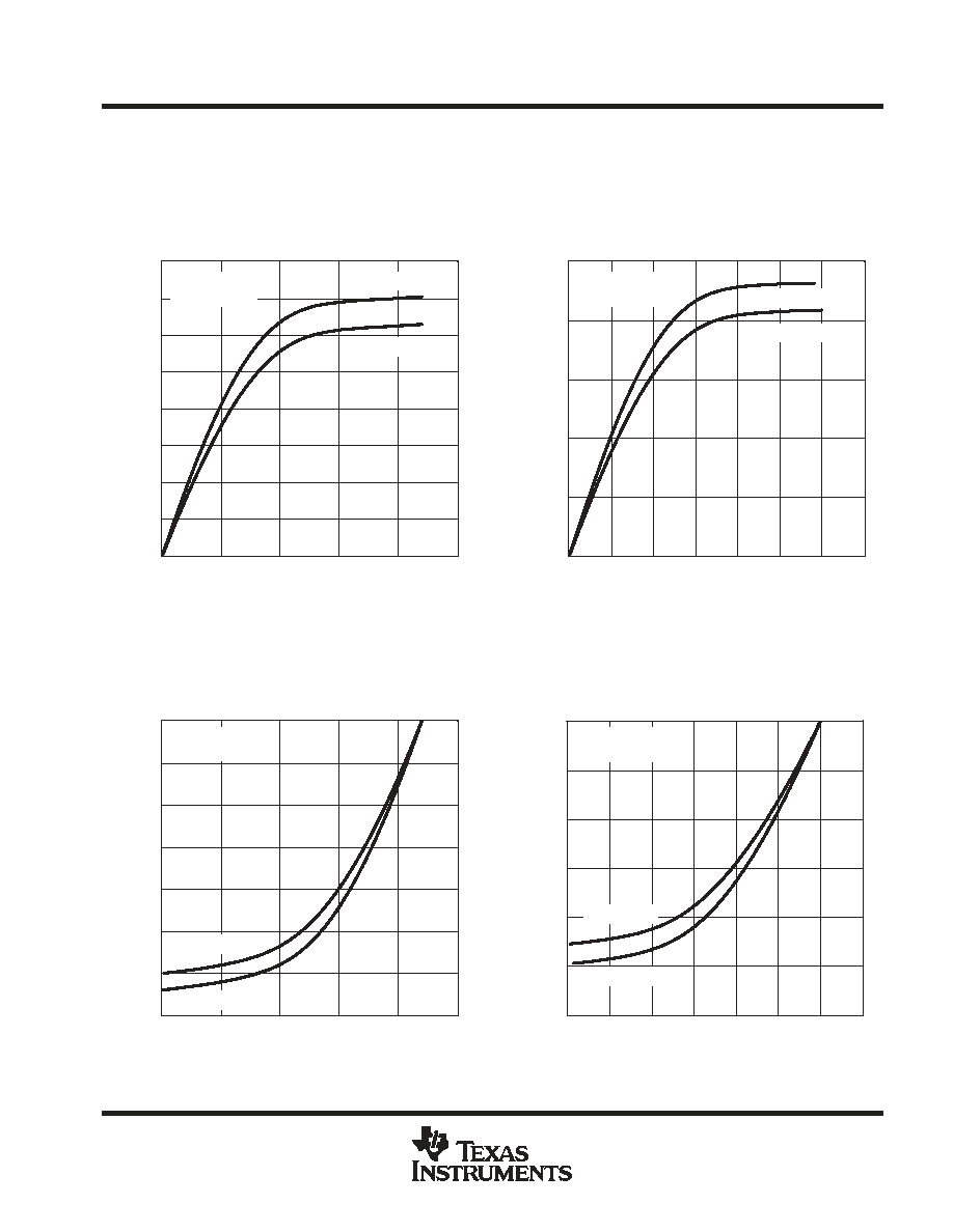
MSP430x412, MSP430x413 outputs - Ports P1, P2, P3, P4, P5, and P6 (see Note)
VOL - Low-Level Output Voltage - V
0
2
4
6
8
10
12
14
16
0.0
0.5
1.0
1.5
2.0
2.5
VCC = 2.2 V
P1.0
TYPICAL LOW-LEVEL OUTPUT CURRENT
vs
LOW-LEVEL OUTPUT VOLTAGE
TA = 25
∞
C
TA = 85
∞
C
I OL
-
T
ypical Low-Level Output Current - mA
Figure 2
VOL - Low-Level Output Voltage - V
0
5
10
15
20
25
0.0
0.5
1.0
1.5
2.0
2.5
3.0
3.5
VCC = 3 V
P1.0
TYPICAL LOW-LEVEL OUTPUT CURRENT
vs
LOW-LEVEL OUTPUT VOLTAGE
TA = 25
∞
C
TA = 85
∞
C
I OL
-
T
ypical Low-Level Output Current - mA
Figure 3
VOH - High-Level Output Voltage - V
-14
-12
-10
-8
-6
-4
-2
0
0.0
0.5
1.0
1.5
2.0
2.5
VCC = 2.2 V
P1.0
TYPICAL HIGH-LEVEL OUTPUT CURRENT
vs
HIGH-LEVEL OUTPUT VOLTAGE
TA = 25
∞
C
TA = 85
∞
C
I OH
-
T
ypical High-Level Output Current - mA
Figure 4
VOH - High-Level Output Voltage - V
-30
-25
-20
-15
-10
-5
0
0.0
0.5
1.0
1.5
2.0
2.5
3.0
3.5
VCC = 3 V
P1.0
TYPICAL HIGH-LEVEL OUTPUT CURRENT
vs
HIGH-LEVEL OUTPUT VOLTAGE
TA = 25
∞
C
TA = 85
∞
C
I OH
-
T
ypical High-Level Output Current - mA
Figure 5
NOTE A: One output loaded at a time
MSP430x41x
MIXED SIGNAL MICROCONTROLLER
SLAS340G - MAY 2001 - REVISED JUNE 2004
26
POST OFFICE BOX 655303
∑
DALLAS, TEXAS 75265
electrical characteristics over recommended operating free-air temperature (unless otherwise
noted) (continued)
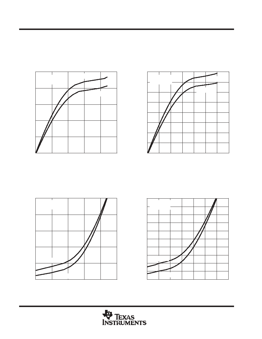
MSP430x415, MSP430x417 outputs - Ports P1, P2, P3, P4, P5, and P6 (see Note)
VOL - Low-Level Output Voltage - V
0
5
10
15
20
25
0.0
0.5
1.0
1.5
2.0
2.5
VCC = 2.2 V
P2.4
TYPICAL LOW-LEVEL OUTPUT CURRENT
vs
LOW-LEVEL OUTPUT VOLTAGE
TA = 25
∞
C
TA = 85
∞
C
I OL
-
T
ypical Low-Level Output Current - mA
Figure 6
d
VOL - Low-Level Output Voltage - V
0
5
10
15
20
25
30
35
40
0.0
0.5
1.0
1.5
2.0
2.5
3.0
3.5
VCC = 3 V
P2.4
TYPICAL LOW-LEVEL OUTPUT CURRENT
vs
LOW-LEVEL OUTPUT VOLTAGE
TA = 25
∞
C
TA = 85
∞
C
I OL
-
T
ypical Low-Level Output Current - mA
Figure 7
VOH - High-Level Output Voltage - V
-25
-20
-15
-10
-5
0
0.0
0.5
1.0
1.5
2.0
2.5
VCC = 2.2 V
P2.4
TYPICAL HIGH-LEVEL OUTPUT CURRENT
vs
HIGH-LEVEL OUTPUT VOLTAGE
TA = 25
∞
C
TA = 85
∞
C
I OH
-
T
ypical High-Level Output Current - mA
Figure 8
VOH - High-Level Output Voltage - V
-50
-45
-40
-35
-30
-25
-20
-15
-10
-5
0
0.0
0.5
1.0
1.5
2.0
2.5
3.0
3.5
VCC = 3 V
P2.4
TYPICAL HIGH-LEVEL OUTPUT CURRENT
vs
HIGH-LEVEL OUTPUT VOLTAGE
TA = 25
∞
C
TA = 85
∞
C
I OH
-
T
ypical High-Level Output Current - mA
Figure 9
NOTE B: One output loaded at a time
MSP430x41x
MIXED SIGNAL MICROCONTROLLER
SLAS340G - MAY 2001 - REVISED JUNE 2004
27
POST OFFICE BOX 655303
∑
DALLAS, TEXAS 75265
electrical characteristics over recommended operating free-air temperature (unless otherwise
noted) (continued)
wake-up LPM3
PARAMETER
TEST CONDITIONS
MIN
TYP
MAX
UNIT
f = 1 MHz
6
td(LPM3)
Delay time
f = 2 MHz
VCC = 2.2 V/3 V
6
µ
s
td(LPM3)
Delay time
f = 3 MHz
VCC = 2.2 V/3 V
6
µ
s
RAM (see Note 1)
PARAMETER
TEST CONDITIONS
MIN
TYP
MAX
UNIT
VRAMh
CPU halted (see Note 1)
1.6
V
NOTE 1: This parameter defines the minimum supply voltage when the data in the program memory RAM remain unchanged. No program
execution should take place during this supply voltage condition.
LCD
PARAMETER
TEST CONDITIONS
MIN
TYP
MAX
UNIT
V(33)
Voltage at P5.7/R33
2.5
VCC +0.2
V(23)
Analog voltage
Voltage at P5.6/R23
VCC = 3 V
(V33-V03)
◊
2/3 + V03
V
V(13)
Analog voltage
Voltage at P5.5/R13
VCC = 3 V
(V(33)-V(03))
◊
1/3 + V(03)
V
V(33) - V(03)
Voltage at R33/R03
2.5
VCC +0.2
I(R03)
R03 = VSS
No load at all
segment and
±
20
I(R13)
Input leakage
P5.5/R13 = VCC/3
No load at all
segment and
common lines,
±
20
nA
I(R23)
Input leakage
P5.6/R23 = 2
◊
VCC/3
common lines,
VCC = 3 V
±
20
nA
V(Sxx0)
V(03)
V(03) - 0.1
V(Sxx1)
Segment line
I(Sxx) = -3 A,
VCC = 3 V
V(13)
V(13) - 0.1
V
V(Sxx2)
Segment line
voltage
I(Sxx) = -3
µ
A,
VCC = 3 V
V(23)
V(23) - 0.1
V
V(Sxx3)
voltage
V(33)
V(33) + 0.1
MSP430x41x
MIXED SIGNAL MICROCONTROLLER
SLAS340G - MAY 2001 - REVISED JUNE 2004
28
POST OFFICE BOX 655303
∑
DALLAS, TEXAS 75265
electrical characteristics over recommended operating free-air temperature (unless otherwise
noted) (continued)
Comparator_A (see Note 1)
PARAMETER
TEST CONDITIONS
MIN
TYP
MAX
UNIT
I(CC)
CAON = 1, CARSEL = 0, CAREF = 0
VCC = 2.2 V
25
40
A
I(CC)
CAON = 1, CARSEL = 0, CAREF = 0
VCC = 3 V
45
60
µ
A
I(Refladder/RefDiode)
CAON = 1, CARSEL = 0,
CAREF = 1/2/3,
VCC = 2.2 V
30
50
A
I(Refladder/RefDiode)
CAREF = 1/2/3,
No load at P1.6/CA0 and P1.7/CA1
VCC = 3 V
45
71
µ
A
V(Ref025)
Voltage @ 0.25 V
CC
node
V
CC
PCA0 = 1, CARSEL = 1, CAREF = 1,
No load at P1.6/CA0 and P1.7/CA1
VCC = 2.2 V / 3 V
0.23
0.24
0.25
V(Ref050)
Voltage @ 0.5 V
CC
node
V
CC
PCA0 = 1, CARSEL = 1, CAREF = 2,
No load at P1.6/CA0 and P1.7/CA1
VCC = 2.2V / 3 V
0.47
0.48
0.50
V(RefVT)
(see Figure 10 and
PCA0 = 1, CARSEL = 1, CAREF = 3,
No load at P1.6/CA0 and P1.7/CA1;
VCC = 2.2 V
390
480
540
mV
V(RefVT)
(see Figure 10 and
Figure 11)
No load at P1.6/CA0 and P1.7/CA1;
TA = 85
∞
C
VCC = 3.0 V
400
490
550
mV
V(IC)
Common-mode input
voltage range
CAON = 1
VCC = 2. 2V/3 V
0
VCC-1.0
V
V(offset)
Offset voltage
See Note 2
VCC = 2.2 V/3 V
-30
30
mV
Vhys
Input hysteresis
CAON = 1
VCC = 2.2 V / 3 V
0
0.7
1.4
mV
TA = 25
∞
C,
VCC = 2.2 V
160
210
300
ns
t(response LH)
TA = 25 C,
Overdrive 10 mV, without filter: CAF = 0
VCC = 3 V
80
150
240
ns
t(response LH)
TA = 25
∞
C
VCC = 2.2 V
1.4
1.9
3.4
s
TA = 25 C
Overdrive 10 mV, with filter: CAF = 1
VCC = 3 V
0.9
1.5
2.6
µ
s
TA = 25
∞
C
VCC = 2.2 V
130
210
300
ns
t(response HL)
TA = 25 C
Overdrive 10 mV, without filter: CAF = 0
VCC = 3 V
80
150
240
ns
t(response HL)
TA = 25
∞
C,
VCC = 2.2 V
1.4
1.9
3.4
s
TA = 25 C,
Overdrive 10 mV, with filter: CAF = 1
VCC = 3.0 V
0.9
1.5
2.6
µ
s
NOTES:
1. The leakage current for the Comparator_A terminals is identical to Ilkg(Px.x) specification.
2. The input offset voltage can be cancelled by using the CAEX bit to invert the Comparator_A inputs on successive measurements.
The two successive measurements are then summed together.
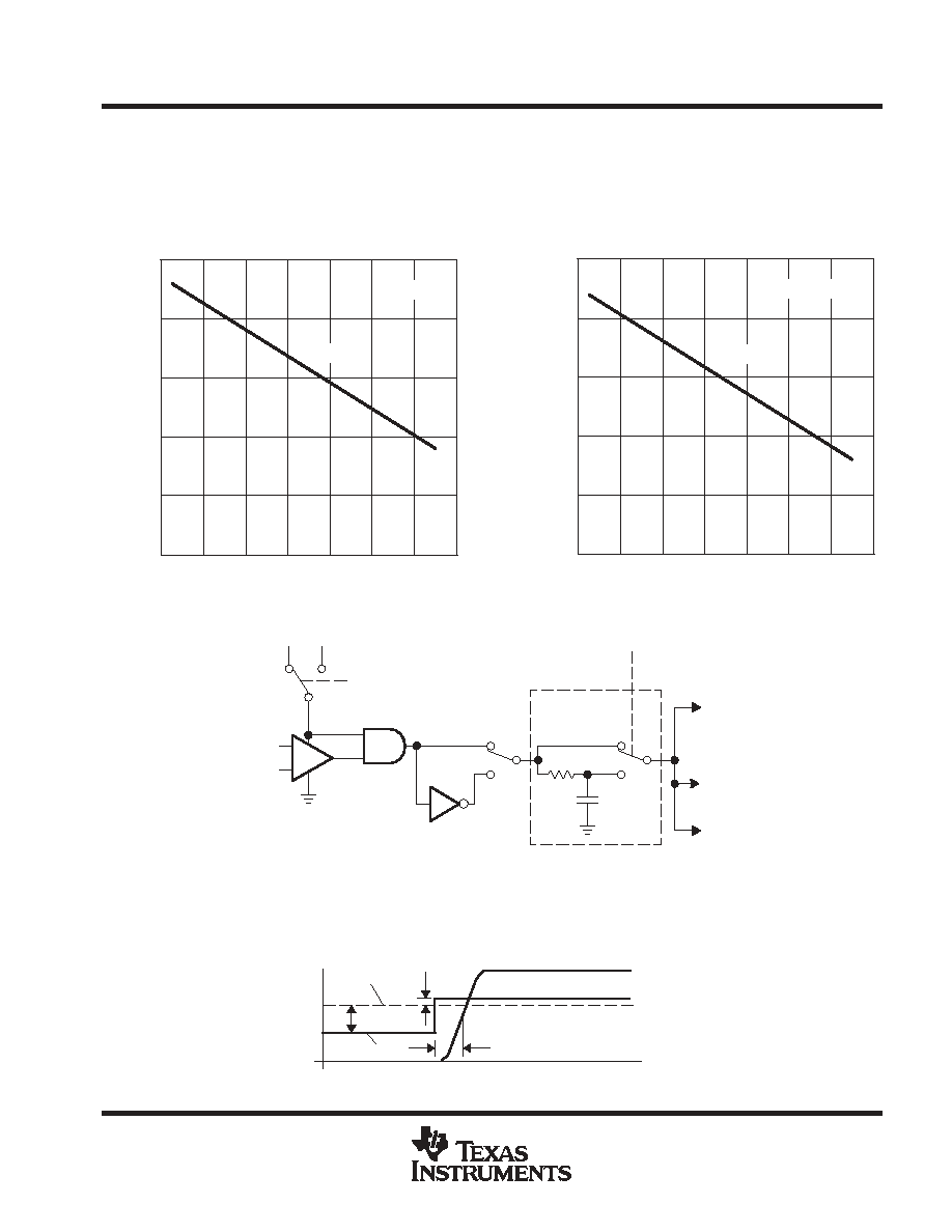
MSP430x41x
MIXED SIGNAL MICROCONTROLLER
SLAS340G - MAY 2001 - REVISED JUNE 2004
29
POST OFFICE BOX 655303
∑
DALLAS, TEXAS 75265
electrical characteristics over recommended operating free-air temperature (unless otherwise
noted) (continued)
TA - Free-Air Temperature -
∞
C
400
450
500
550
600
650
-45
-25
-5
15
35
55
75
95
VCC = 3 V
Typical
V
(RefVT)
- Reference V
oltage - mV
REFERENCE VOLTAGE
vs
FREE-AIR TEMPERATURE
Figure 10
TA - Free-Air Temperature -
∞
C
400
450
500
550
600
650
-45
-25
-5
15
35
55
75
95
VCC = 2.2 V
Typical
V
(RefVT)
- Reference V
oltage - mV
REFERENCE VOLTAGE
vs
FREE-AIR TEMPERATURE
Figure 11
_
+
CAON
0
1
V+
0
1
CAF
Low Pass Filter
2
µ
s
To Internal
Modules
Set CAIFG
Flag
CAOUT
V-
VCC
1
0 V
0
Figure 12. Block Diagram of Comparator_A Module
Overdrive
VCAOUT
t(response)
V+
V-
400 mV
Figure 13. Overdrive Definition
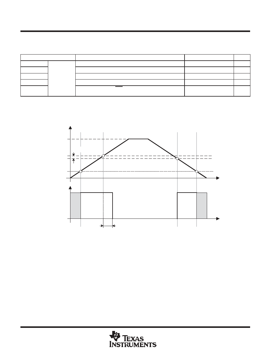
MSP430x41x
MIXED SIGNAL MICROCONTROLLER
SLAS340G - MAY 2001 - REVISED JUNE 2004
30
POST OFFICE BOX 655303
∑
DALLAS, TEXAS 75265
electrical characteristics over recommended operating free-air temperature (unless otherwise
noted) (continued)
POR brownout, reset (see Notes 1 and 2)
PARAMETER
TEST CONDITIONS
MIN
TYP
MAX
UNIT
td(BOR)
2000
µ
s
VCC(start)
dVCC/dt
3 V/s (see Figure 14)
0.7
◊
V(B_IT-)
V
V(B_IT-)
Brownout
dVCC/dt
3 V/s (see Figure 14, Figure 15, Figure 16)
1.71
V
Vhys(B_IT-)
Brownout
dVCC/dt
3 V/s (see Figure 14)
70
130
180
mV
t(reset)
Pulse length needed at RST/NMI pin to accepted reset internally,
VCC = 2.2 V/3 V
2
µ
s
NOTES:
1. The current consumption of the brownout module is already included in the ICC current consumption data. The voltage level V(B_IT-)
+ Vhys(B_IT-) is
1.8 V.
2. During power up, the CPU begins code execution following a period of td(BOR) after VCC = V(B_IT-) + Vhys(B_IT-). The default
FLL+ settings must not be changed until VCC
VCC(min). See the MSP430x4xx Family User's Guide (SLAU056) for more information
on the brownout/SVS circuit.
0
1
V
VCC(start)
Vhys(B_IT-)
VCC
td(BOR)
(B_IT-)
Figure 14. POR/Brownout Reset (BOR) vs Supply Voltage
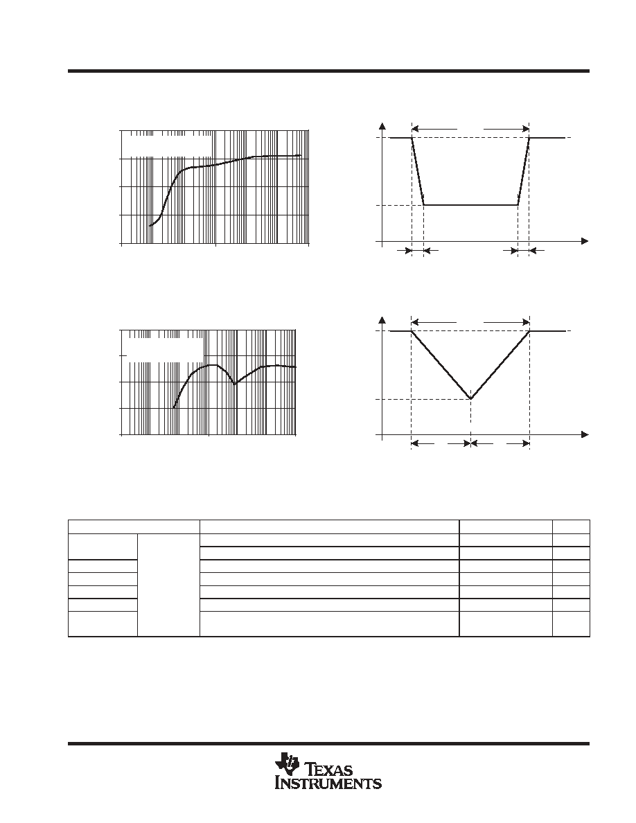
MSP430x41x
MIXED SIGNAL MICROCONTROLLER
SLAS340G - MAY 2001 - REVISED JUNE 2004
31
POST OFFICE BOX 655303
∑
DALLAS, TEXAS 75265
electrical characteristics over recommended operating free-air temperature (unless otherwise
noted) (continued)
V
CC
(min) - V
0
0.5
1
1.5
2
0.001
1
1000
V = 3 V
Typical Conditions
1 ns
1 ns
tpw - Pulse Width -
µ
s
tpw - Pulse Width -
µ
s
cc
VCC
3 V
VCC(min)
tpw
Figure 15. V
CC(min)
Level With a Square Voltage Drop to Generate a POR/Brownout Signal
VCC
3 V
VCC(min)
tpw
0
0.5
1
1.5
2
tpw - Pulse Width -
µ
s
0.001
1
1000
tf
tr
tpw - Pulse Width -
µ
s
tf = tr
V = 3 V
Typical Conditions
cc
V
CC
(min) - V
Figure 16. V
CC(min)
Level With a Triangle Voltage Drop to Generate a POR/Brownout Signal
SVS (supply voltage supervisor/monitor, see Notes 1 and 2) MSP430x412, MSP430x413 only
PARAMETER
TEST CONDITIONS
MIN
TYP
MAX
UNIT
td(SVSR)
dVCC/dt > 30V/ms (see Note 2)
5
150
µ
s
td(SVSR)
dVCC/dt
30V/ms (see Note 2)
2000
µ
s
td(SVSon)
SVSon, switch from 0 to 1, VCC = 3 V (see Note 2)
20
150
µ
s
V(SVSstart)
SVS
dVCC/dt
3 V/s (see Figure 17)
1.55
1.7
V
V(SVS_IT-)
SVS
dVCC/dt
3 V/s (see Figure 17)
1.8
1.95
2.2
V
Vhys(SVS_IT-)
dVCC/dt
3 V/s (see Figure 17)
70
100
155
mV
ICC(SVS)
(see Note 1)
VLD
0 (VLD bits are in SVSCTL register), VCC = 2.2V/ 3V
10
15
µ
A
NOTES:
1. The current consumption of the SVS module is not included in the ICC current consumption data.
2. The SVS is not active at power up.
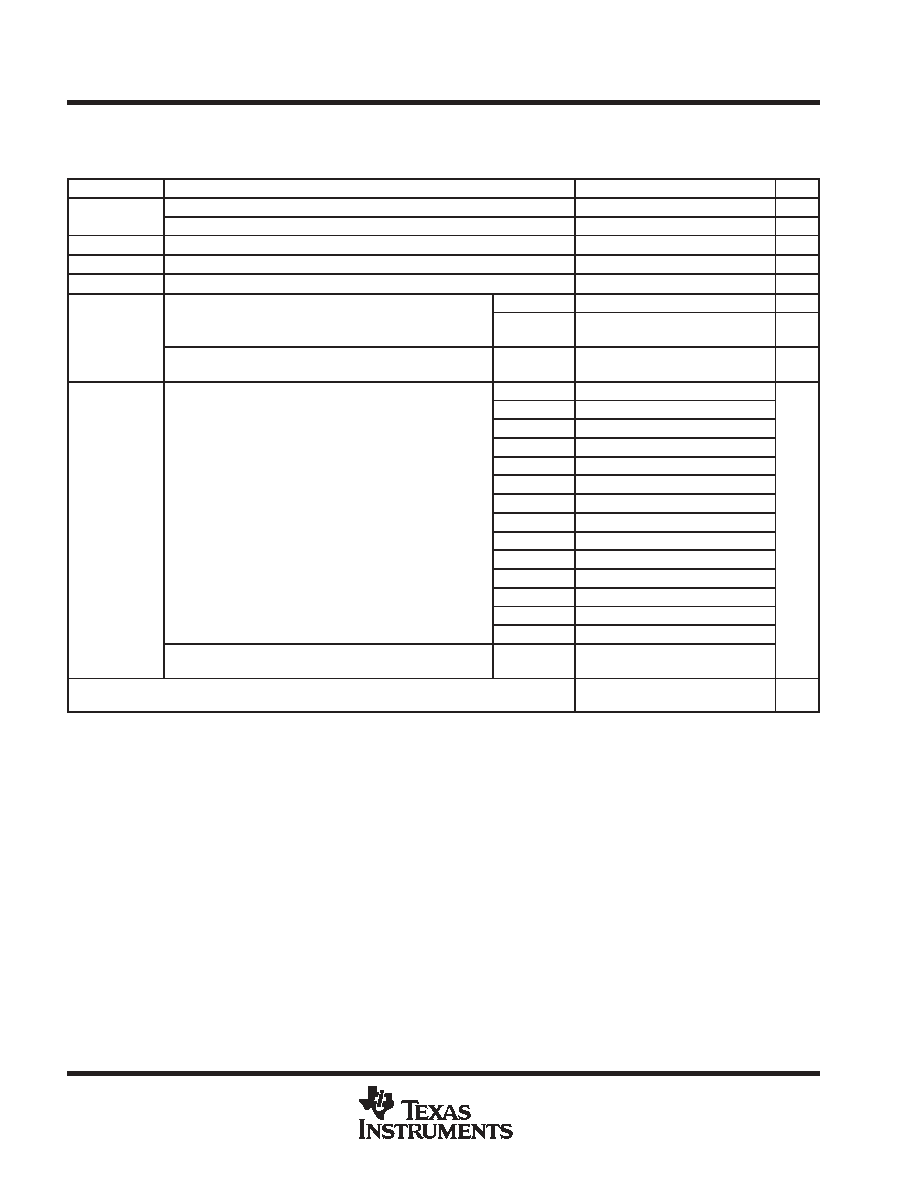
MSP430x41x
MIXED SIGNAL MICROCONTROLLER
SLAS340G - MAY 2001 - REVISED JUNE 2004
32
POST OFFICE BOX 655303
∑
DALLAS, TEXAS 75265
electrical characteristics over recommended operating free-air temperature (unless otherwise
noted) (continued)
SVS (supply voltage supervisor/monitor, see Notes 1 and 2) MSP430x415, MSP430x417 only
PARAMETER
TEST CONDITIONS
MIN
NOM
MAX
UNIT
td(SVSR)
dVCC/dt
>
30 V/ms (see Figure 17)
5
150
µ
s
td(SVSR)
dVCC/dt
30 V/ms
2000
µ
s
td(SVSon)
SVSon, switch from VLD=0 to VLD
0, VCC = 3 V
20
150
µ
s
tsettle
VLD
0
12
µ
s
V(SVSstart)
VLD
0, VCC/dt
3 V/s (see Figure 17)
1.55
1.7
V
VLD = 1
70
120
155
mV
Vhys(SVS_IT-)
VCC/dt
3 V/s (see Figure 17)
VLD = 2 .. 14
V(SVS_IT-)
x 0.004
V(SVS_IT-)
x 0.008
Vhys(SVS_IT-)
VCC/dt
3 V/s (see Figure 17), external voltage applied
on SVSIN
VLD = 15
4.4
10.4
mV
VLD = 1
1.8
1.9
2.05
VLD = 2
1.94
2.1
2.25
VLD = 3
2.05
2.2
2.37
VLD = 4
2.14
2.3
2.48
VLD = 5
2.24
2.4
2.6
VLD = 6
2.33
2.5
2.71
VCC/dt
3 V/s (see Figure 17)
VLD = 7
2.46
2.65
2.86
V(SVS_IT-)
VCC/dt
3 V/s (see Figure 17)
VLD = 8
2.58
2.8
3
V
V(SVS_IT-)
VLD = 9
2.69
2.9
3.13
V
VLD = 10
2.83
3.05
3.29
VLD = 11
2.94
3.2
3.42
VLD = 12
3.11
3.35
3.61
VLD = 13
3.24
3.5
3.76
VLD = 14
3.43
3.7
3.99
VCC/dt
3 V/s (see Figure 17), external voltage applied
on SVSIN
VLD = 15
1.1
1.2
1.3
ICC(SVS)
(see Note 1)
VLD
0, VCC = 2.2 V/3 V
10
15
µ
A
The recommended operating voltage range is limited to 3.6 V.
tsettle is the settling time that the comparator o/p needs to have a stable level after VLD is switched VLD
0 to a different VLD value somewhere
between 2 and 15. The overdrive is assumed to be > 50 mV.
NOTES:
1. The current consumption of the SVS module is not included in the ICC current consumption data.
2. The SVS is not active at power up.
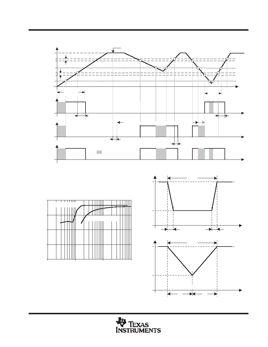
MSP430x41x
MIXED SIGNAL MICROCONTROLLER
SLAS340G - MAY 2001 - REVISED JUNE 2004
33
POST OFFICE BOX 655303
∑
DALLAS, TEXAS 75265
electrical characteristics over recommended operating free-air temperature (unless otherwise
noted) (continued)
VCC(start)
VCC
V(B_IT-)
Brownout
Region
V(SVSstart)
V
Software Sets VLD>0:SVS is Active
Undefined
0
1
Brownout
0
1
0
1
Set POR
Brownout
Region
SVS Circuit is Active From VLD > to V
CC
< V
(B_IT-)
SVS out
Vhys(SVS_IT-)
V
hys(B_IT-)
td(BOR)
td(SVSon)
td(SVSR)
td(BOR)
(SVS_IT-)
Figure 17. SVS Reset (SVSR) vs Supply Voltage
VCC(min)
0
0.5
1
1.5
2
1 ns
1 ns
tpw - Pulse Width -
µ
s
1
10
1000
tf
tr
t - Pulse Width -
µ
s
100
tf = tr
Rectangular Drop
V
CC(min)
- V
Triangular Drop
3 V
VCC
tpw
3 V
VCC
tpw
VCC(min)
Figure 18. V
CC(min)
With a Square Voltage Drop and a Triangle Voltage Drop to Generate an SVS Signal
MSP430x41x
MIXED SIGNAL MICROCONTROLLER
SLAS340G - MAY 2001 - REVISED JUNE 2004
34
POST OFFICE BOX 655303
∑
DALLAS, TEXAS 75265
electrical characteristics over recommended operating free-air temperature (unless otherwise
noted) (continued)
DCO
PARAMETER
TEST CONDITIONS
VCC
MIN
TYP
MAX
UNIT
f(DCOCLK)
N(DCO)=01E0h, FN_8=FN_4=FN_3=FN_2=0, D = 2; DCOPLUS= 0
2.2 V/3 V
1
MHz
f(DCO2)
FN_8=FN_4=FN_3=FN_2=0 ; DCOPLUS = 1
2.2 V
0.3
0.65
1.25
MHz
f(DCO2)
FN_8=FN_4=FN_3=FN_2=0 ; DCOPLUS = 1
3 V
0.3
0.7
1.3
MHz
f(DCO27)
FN_8=FN_4=FN_3=FN_2=0; DCOPLUS = 1, (see Note 1)
2.2 V
2.5
5.6
10.5
MHz
f(DCO27)
FN_8=FN_4=FN_3=FN_2=0; DCOPLUS = 1, (see Note 1)
3 V
2.7
6.1
11.3
MHz
f(DCO2)
FN_8=FN_4=FN_3=0, FN_2=1; DCOPLUS = 1
2.2 V
0.7
1.3
2.3
MHz
f(DCO2)
FN_8=FN_4=FN_3=0, FN_2=1; DCOPLUS = 1
3 V
0.8
1.5
2.5
MHz
f(DCO27)
FN_8=FN_4=FN_3=0, FN_2=1; DCOPLUS = 1, (see Note 1)
2.2 V
5.7
10.8
18
MHz
f(DCO27)
FN_8=FN_4=FN_3=0, FN_2=1; DCOPLUS = 1, (see Note 1)
3 V
6.5
12.1
20
MHz
f(DCO2)
FN_8=FN_4=0, FN_3= 1, FN_2=x; DCOPLUS = 1
2.2 V
1.2
2
3
MHz
f(DCO2)
FN_8=FN_4=0, FN_3= 1, FN_2=x; DCOPLUS = 1
3 V
1.3
2.2
3.5
MHz
f(DCO27)
FN_8=FN_4=0, FN_3= 1, FN_2=x; DCOPLUS = 1, (see Note 1)
2.2 V
9
15.5
25
MHz
f(DCO27)
FN_8=FN_4=0, FN_3= 1, FN_2=x; DCOPLUS = 1, (see Note 1)
3 V
10.3
17.9
28.5
MHz
f(DCO2)
FN_8=0, FN_4= 1, FN_3= FN_2=x; DCOPLUS = 1
2.2 V
1.8
2.8
4.2
MHz
f(DCO2)
FN_8=0, FN_4= 1, FN_3= FN_2=x; DCOPLUS = 1
3 V
2.1
3.4
5.2
MHz
f(DCO27)
FN_8=0, FN_4=1, FN_3= FN_2=x; DCOPLUS = 1, (see Note 1)
2.2 V
13.5
21.5
33
MHz
f(DCO27)
FN_8=0, FN_4=1, FN_3= FN_2=x; DCOPLUS = 1, (see Note 1)
3 V
16
26.6
41
MHz
f(DCO2)
FN_8=1, FN_4=FN_3=FN_2=x; DCOPLUS = 1
2.2 V
2.8
4.2
6.2
MHz
f(DCO2)
FN_8=1, FN_4=FN_3=FN_2=x; DCOPLUS = 1
3 V
4.2
6.3
9.2
MHz
f(DCO27)
FN_8=1,FN_4=FN_3=FN_2=x; DCOPLUS = 1, (see Note 1)
2.2 V
21
32
46
MHz
f(DCO27)
FN_8=1,FN_4=FN_3=FN_2=x; DCOPLUS = 1, (see Note 1)
3 V
30
46
70
MHz
Sn
Step size between adjacent DCO taps:
1 < TAP
20
1.06
1.11
Sn
Step size between adjacent DCO taps:
Sn = fDCO(Tap n+1) / fDCO(Tap n), (see Figure 20 for taps 21 to 27)
TAP = 27
1.07
1.17
Dt
Temperature drift, N(DCO) = 01E0h, FN_8=FN_4=FN_3=FN_2=0
2.2 V
≠0.2
≠0.3
≠0.4
%
/_
C
Dt
Temperature drift, N(DCO) = 01E0h, FN_8=FN_4=FN_3=FN_2=0
D = 2; DCOPLUS = 0, (see Note 2)
3 V
≠0.2
≠0.3
≠0.4
%
/_
C
DV
Drift with VCC variation, N(DCO) = 01E0h, FN_8=FN_4=FN_3=FN_2=0
D = 2; DCOPLUS = 0 (see Note 2)
0
5
15
%/V
NOTES:
1. Do not exceed the maximum system frequency.
2. This parameter is not production tested.
TA -
∞
C
VCC - V
f
(DCO)
f
(DCO20
5
C)
f
(DCO)
f
(DCO3V)
1.8
3.0
2.4
3.6
1.0
20
60
40
85
1.0
0
-20
-40
0
Figure 19. DCO Frequency vs Supply Voltage V
CC
and vs Ambient Temperature
MSP430x41x
MIXED SIGNAL MICROCONTROLLER
SLAS340G - MAY 2001 - REVISED JUNE 2004
35
POST OFFICE BOX 655303
∑
DALLAS, TEXAS 75265
electrical characteristics over recommended operating free-air temperature (unless otherwise
noted) (continued)
ŒŒŒŒŒŒŒŒŒŒŒŒŒ
ŒŒŒŒŒŒŒŒŒŒŒŒŒ
ŒŒŒŒŒŒŒŒŒŒŒŒŒ
ŒŒŒŒŒŒŒŒŒŒŒŒŒ
ŒŒŒŒŒŒŒŒŒŒŒŒŒ
ŒŒŒŒŒŒŒŒŒŒŒŒŒ
ŒŒŒŒŒŒŒŒŒŒŒŒŒ
ŒŒŒŒŒŒŒŒŒŒŒŒŒ
ŒŒŒŒŒŒŒŒŒŒŒŒŒ
ŒŒŒŒŒŒŒŒŒŒŒŒŒ
1
27
20
1.11
1.17
DCO Tap
S
n
- Stepsize Ratio between DCO T
aps
Min
Max
1.07
1.06
Figure 20. DCO Tap Step Size
DCO Frequency
Adjusted by Bits
29 to 25 in SCFI1 {N{DCO}}
FN_2=0
FN_3=0
FN_4=0
FN_8=0
FN_2=1
FN_3=0
FN_4=0
FN_8=0
FN_2=x
FN_3=1
FN_4=0
FN_8=0
FN_2=x
FN_3=x
FN_4=1
FN_8=0
FN_2=x
FN_3=x
FN_4=x
FN_8=1
Legend
Tolerance at Tap 27
Tolerance at Tap 2
Overlapping DCO Ranges:
Uninterrupted Frequency Range
f (DCO)
Figure 21. Five Overlapping DCO Ranges Controlled by FN_x Bits
MSP430x41x
MIXED SIGNAL MICROCONTROLLER
SLAS340G - MAY 2001 - REVISED JUNE 2004
36
POST OFFICE BOX 655303
∑
DALLAS, TEXAS 75265
electrical characteristics over recommended operating free-air temperature (unless otherwise
noted) (continued)
crystal oscillator, LFXT1 oscillator (see Notes 1 and 2)
PARAMETER
TEST CONDITIONS
VCC
MIN
TYP
MAX
UNIT
OSCCAPx = 0h
2.2 V/3 V
0
CXIN
Integrated load capacitance
OSCCAPx = 1h
2.2 V/3 V
10
pF
CXIN
Integrated load capacitance
OSCCAPx = 2h
2.2 V/3 V
14
pF
OSCCAPx = 3h
2.2 V/3 V
18
OSCCAPx = 0h
2.2 V/3 V
0
CXOUT
Integrated load capacitance
OSCCAPx = 1h
2.2 V/3 V
10
pF
CXOUT
Integrated load capacitance
OSCCAPx = 2h
2.2 V/3 V
14
pF
OSCCAPx = 3h
2.2 V/3 V
18
VIL
Input levels at XIN
see Note 3
2.2 V/3 V
VSS
0.2
◊
VCC
V
VIH
Input levels at XIN
see Note 3
2.2 V/3 V
0.8
◊
VCC
VCC
V
NOTES:
1. The parasitic capacitance from the package and board may be estimated to be 2pF. The effective load capacitor for the crystal is
(CXIN x CXOUT) / (CXIN + CXOUT). It is independent of XTS_FLL.
2. To improve EMI on the low-power LFXT1 oscillator, particularly in the LF mode (32 kHz), the following guidelines must be
observed:
∑
Keep as short a trace as possible between the 'x41x and the crystal.
∑
Design a good ground plane around oscillator pins.
∑
Prevent crosstalk from other clock or data lines into oscillator pins XIN and XOUT.
∑
Avoid running PCB traces underneath or adjacent to XIN an XOUT pins.
∑
Use assembly materials and praxis to avoid any parasitic load on the oscillator XIN and XOUT pins.
∑
If conformal coating is used, ensure that it does not induce capacitive/resistive leakage between the oscillator pins.
∑
Do not route the XOUT line to the JTAG header to support the serial programming adapter as shown in other documentation.
This signal is no longer required for the serial programming adapter.
3. Applies only when using an external logic-level clock source. XTS_FLL must be set. Not applicable when using a crystal or resonator.
MSP430x41x
MIXED SIGNAL MICROCONTROLLER
SLAS340G - MAY 2001 - REVISED JUNE 2004
37
POST OFFICE BOX 655303
∑
DALLAS, TEXAS 75265
electrical characteristics over recommended operating free-air temperature (unless otherwise
noted) (continued)
Flash Memory
PARAMETER
TEST
CONDITIONS
VCC
MIN
NOM
MAX
UNIT
VCC(PGM/
ERASE)
Program and Erase supply voltage
2.7
3.6
V
fFTG
Flash Timing Generator frequency
257
476
kHz
IPGM
Supply current from DVCC during program
2.7 V/ 3.6 V
3
5
mA
IERASE
Supply current from DVCC during erase
2.7 V/ 3.6 V
3
7
mA
tCPT
Cumulative program time
see Note 1
2.7 V/ 3.6 V
4
ms
tCMErase
Cumulative mass erase time
see Note 2
2.7 V/ 3.6 V
200
ms
Program/Erase endurance
104
105
cycles
tRetention
Data retention duration
TJ = 25
∞
C
100
years
tWord
Word or byte program time
35
tBlock, 0
Block program time for 1st byte or word
30
tBlock, 1-63
Block program time for each additional byte or word
see Note 3
21
tFTG
tBlock, End
Block program end-sequence wait time
see Note 3
6
tFTG
tMass Erase
Mass erase time
5297
tSeg Erase
Segment erase time
4819
NOTES:
1. The cumulative program time must not be exceeded when writing to a 64-byte flash block. This parameter applies to all programming
methods: individual word/byte write and block write modes.
2. The mass erase duration generated by the flash timing generator is at least 11.1ms ( = 5297x1/fFTG,max = 5297x1/476kHz). To
achieve the required cumulative mass erase time the Flash Controller's mass erase operation can be repeated until this time is met.
(A worst case minimum of 19 cycles are required).
3. These values are hardwired into the Flash Controller's state machine (tFTG = 1/fFTG).
JTAG Interface
PARAMETER
TEST
CONDITIONS
VCC
MIN
NOM
MAX
UNIT
fTCK
TCK input frequency
see Note 1
2.2 V
0
5
MHz
fTCK
TCK input frequency
see Note 1
3 V
0
10
MHz
RInternal
Internal pull-up resistance on TMS, TCK, TDI/TCLK
see Note 2
2.2 V/ 3 V
25
60
90
k
NOTES:
1. fTCK may be restricted to meet the timing requirements of the module selected.
2. TMS, TDI/TCLK, and TCK pull-up resistors are implemented in all versions.
JTAG Fuse (see Note 1)
PARAMETER
TEST
CONDITIONS
VCC
MIN
NOM
MAX
UNIT
VCC(FB)
Supply voltage during fuse-blow condition
TA = 25
∞
C
2.5
V
VFB
Voltage level on TDI/TCLK for fuse-blow - 'C41x
3.5
3.9
V
VFB
Voltage level on TDI/TCLK for fuse-blow - 'F41x
6
7
V
IFB
Supply current into TDI/TCLK during fuse blow
100
mA
tFB
Time to blow fuse
1
ms
NOTES:
1. Once the fuse is blown, no further access to the MSP430 JTAG/Test and emulation features is possible. The JTAG block is switched
to bypass mode.
MSP430x41x
MIXED SIGNAL MICROCONTROLLER
SLAS340G - MAY 2001 - REVISED JUNE 2004
38
POST OFFICE BOX 655303
∑
DALLAS, TEXAS 75265
APPLICATION INFORMATION
input/output schematic
Port P1, P1.0 to P1.5, input/output with Schmitt-trigger
TACLK
P1OUT.x
Module X OUT
P1DIR.x
Direction Control
From Module
P1SEL.x
D
EN
Interrupt
Edge
Select
P1IES.x
P1SEL.x
P1IE.x
P1IFG.x
P1IRQ.x
P1.x
EN
Set
Q
0
1
1
0
Pad Logic
0: Input
1: Output
Bus
keeper
CAPD.x
PnSEL.x
PnDIR.x
Direction
From Module
PnOUT.x
Module X
OUT
PnIN.x
PnIE.x
PnIFG.x
PnIES.x
Module X IN
P1SEL.1
P1DIR.1
P1OUT.1
P1IN.1
P1IE.1
P1IFG.1
P1IES.1
P1SEL.2
P1DIR.2
P1OUT.2
P1IN.2
P1IE.2
P1IFG.2
P1IES.2
P1SEL.3
P1DIR.3
P1OUT.3
P1IN.3
P1IE.3
P1IFG.3
P1IES.3
P1SEL.4
P1DIR.4
P1OUT.4
P1IN.4
P1IE.4
P1IFG.4
P1IES.4
P1SEL.5
P1DIR.5
P1OUT.5
P1IN.5
P1IE.5
P1IFG.5
P1IES.5
P1SEL.0
P1DIR.0
P1OUT.0
P1IN.0
P1IE.0
P1IFG.0
P1IES.0
SVSOUT
Unused
Unused
P1DIR.1
P1DIR.2
P1DIR.3
P1DIR.4
P1DIR.5
P1DIR.0
ACLK
MCLK
Module X IN
P1IN.x
P1.5/TACLK/ACLK
P1.0/TA0
P1.1/TA0/MCLK
P1.2/TA1
P1.4
P1.3/SVSOUT
Control
NOTE: 0
x
5.
Port Function is Active if CAPD.x = 0
Timer_A3/Timer0_A3
Timer1_A5 (MSP430x415, MSP430x417 only)
ß MSP430x412, MSP430x413 only
Out0 Sig.
Out1 Sig.
CCI0A
CCI1A
CCI0B
MSP430x412,
MSP430x413 only
MSP430x415,
MSP430x417 only
P1.5/TA0CLK/ACLK
P1.0/TA0.0
P1.1/TA0.0/MCLK
P1.2/TA0.1
P1.4/TA1.0
P1.3/TA1.0/SVSOUT
Out0 Sig.
DVSS
CCI0A
ß
ß
MSP430x41x
MIXED SIGNAL MICROCONTROLLER
SLAS340G - MAY 2001 - REVISED JUNE 2004
39
POST OFFICE BOX 655303
∑
DALLAS, TEXAS 75265
APPLICATION INFORMATION
input/output schematic (continued)
Port P1, P1.6, P1.7 input/output with Schmitt-trigger
Comparator_A
P1OUT.7
DVSS
P1DIR.7
P1SEL.7
D
EN
Interrupt
Edge
Select
P1IES.7
P1SEL.7
P1IE.7
P1IFG.7
P1IRQ.07
EN
Set
Q
0
1
1
0
CAPD.7
P1OUT.6
DVSS
P1DIR.6
P1SEL.6
D
EN
Interrupt
Edge
Select
P1IES.x
P1SEL.x
P1IFG.7
P1IRQ.07
P1.6/
CA0
EN
Set
Q
0
1
1
0
CAPD.6
Note: Port Function Is Active if CAPD.6 = 0
P1IN.6
unused
P1.7/
CA1
Reference Block
CCI1B
CAF
CAREF
P2CA
CAEX
CAREF
to Timer_Ax
-
+
2
AVcc
CA0
CA1
Pad Logic
0: Input
1: Output
Bus
Keeper
Pad Logic
0: Input
1: Output
Bus
Keeper
P1DIR.6
P1DIR.7
P1IN.7
unused
P1IE.7
Note: Port Function Is Active if CAPD.7 = 0
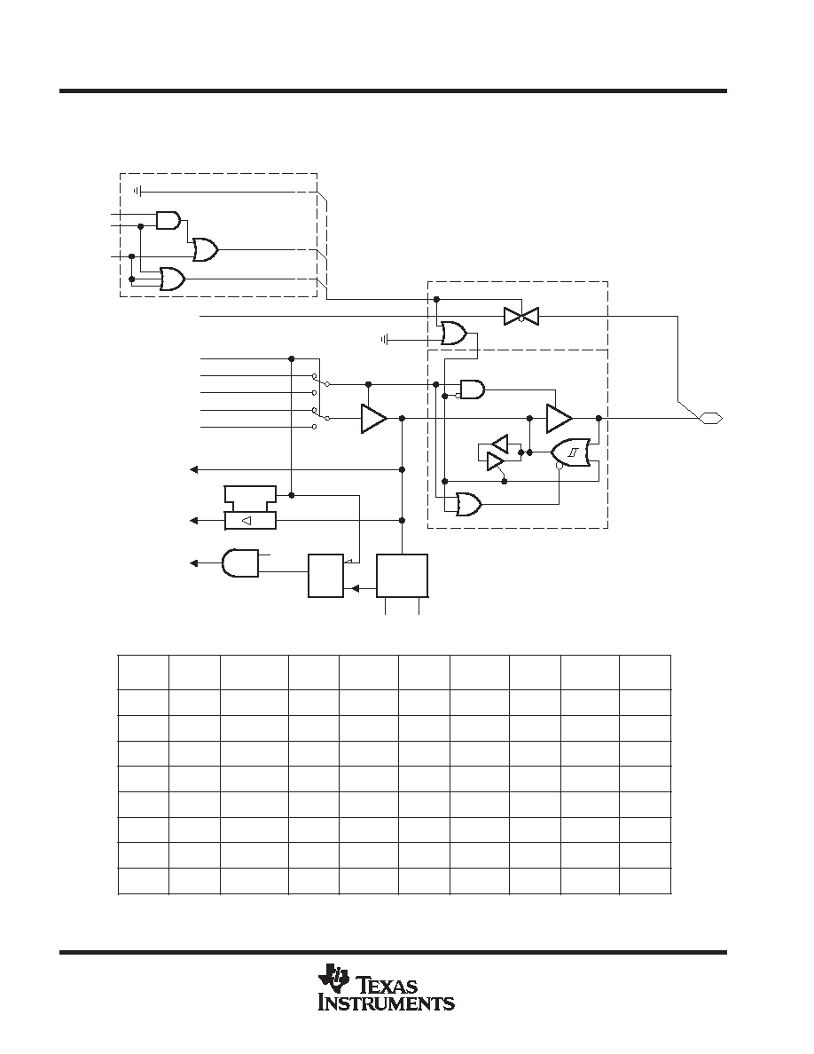
MSP430x41x
MIXED SIGNAL MICROCONTROLLER
SLAS340G - MAY 2001 - REVISED JUNE 2004
40
POST OFFICE BOX 655303
∑
DALLAS, TEXAS 75265
APPLICATION INFORMATION
input/output schematic (continued)
port P2, P2.0 to P2.7, input/output with Schmitt-trigger
P2SEL.1
P2DIR.1
P2OUT.1
P2IN.1
P2IE.1
P2IFG.1
P2IES.1
P2SEL.2
P2DIR.2
P2OUT.2
P2IN.2
P2IE.2
P2IFG.2
P2IES.2
P2SEL.3
P2DIR.3
P2OUT.3
P2IN.3
P2IE.3
P2IFG.3
P2IES.3
P2SEL.4
P2DIR.4
P2OUT.4
P2IN.4
P2IE.4
P2IFG.4
P2IES.4
P2SEL.5
P2DIR.5
P2OUT.5
P2IN.5
P2IE.5
P2IFG.5
P2IES.5
P2SEL.0
P2DIR.0
P2OUT.0
P2IN.0
P2IE.0
P2IFG.0
P2IES.0
P2DIR.1
P2DIR.2
P2DIR.0
0: Port Active
1: Segment xx
P2SEL.6
P2DIR.6
P2SEL.7
P2DIR.7
P2DIR.6
P2DIR.7
P2OUT.6
P2OUT.7
P2IN.6
P2IN.7
CAOUT
P2IE.6
P2IE.7
P2IFG.6
P2IFG.7
P2IES.6
P2IES.7
P2DIR.3
P2DIR.4
P2DIR.5
P2OUT.x
Module X OUT
P2DIR.x
Direction Control
From Module
P2SEL.x
D
EN
Interrupt
Edge
Select
P2IES.x
P2SEL.x
P2IE.x
P2IFG.x
P2IRQ.x
P2.x
EN
Set
Q
0
1
1
0
Pad Logic
0: Input
1: Output
Bus
keeper
PnSEL.x
PnDIR.x
Direction
From Module
PnOUT.x
Module X
OUT
PnIN.x
PnIE.x
PnIFG.x
PnIES.x
Module X IN
Module X IN
P2IN.x
Control
NOTE: 0
x
7
Out2 Sig.
CCI2A
DVSS
DVSS
Unused
Unused
P2.7/S18
P2.6/CAOUT/S19
P2.5/S20
P2.0/TA2
P2.1
P2.2/S23
P2.4/S21
P2.3/S22
Segment xx
Function Active
LCDM.5
LCDM.6
LCDM.7
P2.2 to P2.5
P2.0, P2.1
P2.6, P2.7
MSP430x412,
MSP430x413 only
MSP430x415,
MSP430x417 only
P2.7/S18
P2.6/CAOUT/S19
P2.5/TA1CLK/S20
P2.0/TA0.2
P2.1/TA1.1
P2.2/TA1.2/S23
P2.4/TA1.4/S21
P2.3/TA1.3/S22
Timer_A3/Timer0_A3
Timer1_A5 (MSP430x415, MSP430x417 only)
ß MSP430x412, MSP430x413 only
Out1 Sig.
Out2 Sig.
Out3 Sig.
Out4 Sig.
CCI1A
CCI2A
CCI3A
CCI4A
TA1CLK
DVSSß
DVSSß
DVSSß
DVSSß
Unusedß
Unusedß
Unusedß
Unusedß
Unusedß
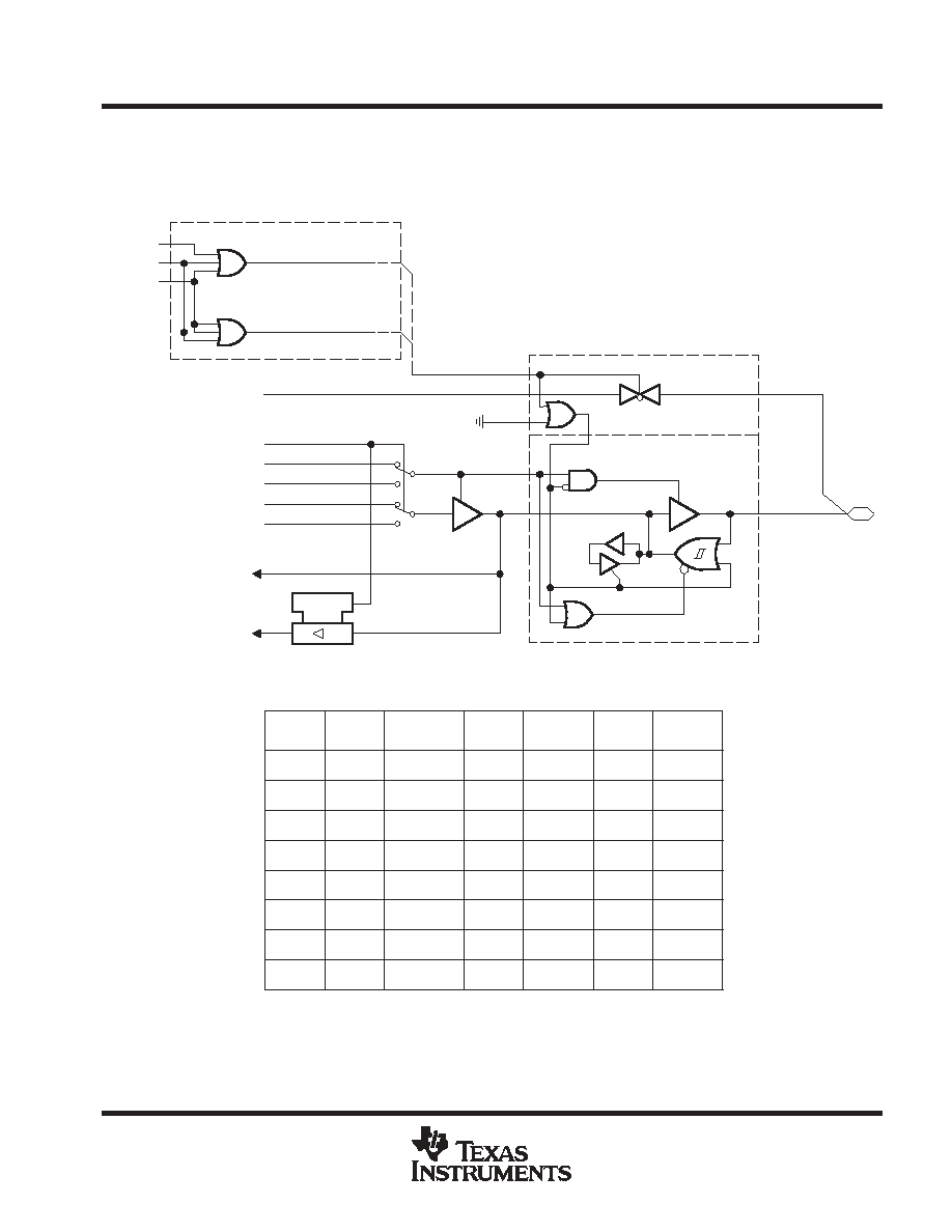
MSP430x41x
MIXED SIGNAL MICROCONTROLLER
SLAS340G - MAY 2001 - REVISED JUNE 2004
41
POST OFFICE BOX 655303
∑
DALLAS, TEXAS 75265
APPLICATION INFORMATION
input/output schematic (continued)
port P3, P3.0, P3.7, input/output with Schmitt-trigger
P3SEL.0
P3DIR.0
P3OUT.0
P3IN.0
0: Port Active
1: Segment xx
DVSS
Unused
P3OUT.x
Module X OUT
P3DIR.x
Direction Control
From Module
P3SEL.x
D
EN
P3.x
0
1
1
0
Pad Logic
0: Input
1: Output
Bus
keeper
PnSEL.x
PnDIR.x
Direction
From Module
PnOUT.x
Module X
OUT
PnIN.x
Module X IN
Module X IN
P3IN.x
Control
NOTE: 0
x
7
DVSS
DVSS
DVSS
DVSS
DVSS
Unused
Unused
Unused
Unused
Unused
Unused
Segment xx
Function Active
LCDM.6
P3.2 to P3.7
P3.0, P3.1
P3.7/S10
P3.6/S11
P3.5/S12
P3.0/S17
P3.1/S16
P3.2/S15
P3.4/S13
P3.3/S14
LCDM.7
LCDM.5
Unused
DVSS
DVSS
P3SEL.1
P3DIR.1
P3OUT.1
P3IN.1
P3SEL.2
P3DIR.2
P3OUT.2
P3IN.2
P3SEL.3
P3DIR.3
P3OUT.3
P3IN.3
P3SEL.4
P3DIR.4
P3OUT.4
P3IN.4
P3SEL.5
P3DIR.5
P3OUT.5
P3IN.5
P3SEL.6
P3DIR.6
P3OUT.6
P3IN.6
P3SEL.7
P3DIR.7
P3OUT.7
P3IN.7
P3DIR.0
P3DIR.1
P3DIR.2
P3DIR.3
P3DIR.4
P3DIR.5
P3DIR.6
P3DIR.7

MSP430x41x
MIXED SIGNAL MICROCONTROLLER
SLAS340G - MAY 2001 - REVISED JUNE 2004
42
POST OFFICE BOX 655303
∑
DALLAS, TEXAS 75265
APPLICATION INFORMATION
input/output schematic (continued)
port P4, P4.0 to P4.7, input/output with Schmitt-trigger
P4SEL.0
P4DIR.0
P4OUT.0
P4IN.0
0: Port Active
1: Segment xx
DVSS
Unused
P4OUT.x
Module X OUT
P4DIR.x
Direction Control
From Module
P4SEL.x
D
EN
P4.x
0
1
1
0
Pad Logic
0: Input
1: Output
Bus
keeper
PnSEL.x
PnDIR.x
Direction
From Module
PnOUT.x
Module X
OUT
PnIN.x
Module X IN
Module X IN
P4IN.x
Control
NOTE: 0
x
7
DVSS
DVSS
DVSS
DVSS
DVSS
Unused
Unused
Unused
Unused
Unused
Unused
Segment xx
Function Active
LCDM.6
LCDM.7
LCDM.5
Unused
DVSS
DVSS
P4.7/S2
P4.6/S3
P4.5/S4
P4.0/S9
P4.1/S8
P4.2/S7
P4.4/S5
P4.3/S6
P4SEL.1
P4DIR.1
P4OUT.1
P4IN.1
P4SEL.2
P4DIR.2
P4OUT.2
P4IN.2
P4SEL.3
P4DIR.3
P4OUT.3
P4IN.3
P4SEL.4
P4DIR.4
P4OUT.4
P4IN.4
P4SEL.5
P4DIR.5
P4OUT.5
P4IN.5
P4SEL.6
P4DIR.6
P4OUT.6
P4IN.6
P4SEL.7
P4DIR.7
P4OUT.7
P4IN.7
P4DIR.0
P4DIR.1
P4DIR.2
P4DIR.3
P4DIR.4
P4DIR.5
P4DIR.6
P4DIR.7
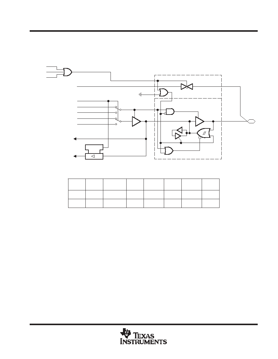
MSP430x41x
MIXED SIGNAL MICROCONTROLLER
SLAS340G - MAY 2001 - REVISED JUNE 2004
43
POST OFFICE BOX 655303
∑
DALLAS, TEXAS 75265
APPLICATION INFORMATION
input/output schematic (continued)
port P5, P5.0, P5.1, input/output with Schmitt-trigger
P5SEL.0
P5DIR.0
P5OUT.0
P5IN.0
S1
P5DIR.0
DVSS
Unused
PnSEL.x
PnDIR.x
Direction
From Module
PnOUT.x
Module X
OUT
PnIN.x
Segment
Module X IN
Control
NOTE: x = 0, 1
0: Port Active
1: Segment
P5OUT.x
Module X OUT
P5DIR.x
Direction Control
From Module
P5SEL.x
D
EN
P5.x
0
1
1
0
Pad Logic
0: Input
1: Output
Bus
keeper
Module X IN
P5IN.x
Segment xx or
Function Active
LCDM.6
LCDM.7
LCDM.5
P5.0/S1
P5.1/S0
COMx or Rxx
DVSS
Unused
P5SEL.1
P5DIR.1
P5OUT.1
P5IN.1
S0
P5DIR.1
DVSS
Unused
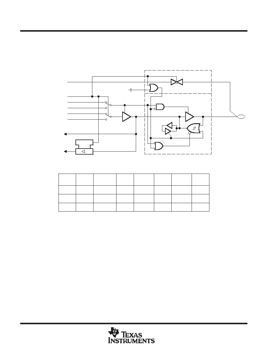
MSP430x41x
MIXED SIGNAL MICROCONTROLLER
SLAS340G - MAY 2001 - REVISED JUNE 2004
44
POST OFFICE BOX 655303
∑
DALLAS, TEXAS 75265
APPLICATION INFORMATION
input/output schematic (continued)
port P5, P5.2, P5.4, input/output with Schmitt-trigger
P5SEL.2
P5DIR.2
P5OUT.2
P5IN.2
COM1
P5DIR.2
DVSS
Unused
PnSEL.x
PnDIR.x
Direction
From Module
PnOUT.x
Module X
OUT
PnIN.x
COMx
Module X IN
Control
NOTE: 2
x
4
DVSS
Unused
0: Port Active
1: COMx Function
P5OUT.x
Module X OUT
P5DIR.x
Direction Control
From Module
P5SEL.x
D
EN
P5.x
0
1
1
0
Pad Logic
0: Input
1: Output
Bus
keeper
Module X IN
P5IN.x
COMx
Active
P5.2/COM1
P5.3/COM2
DVSS
Unused
P5SEL.3
P5DIR.3
P5OUT.3
P5IN.3
COM2
P5DIR.3
DVSS
Unused
P5SEL.4
P5DIR.4
P5OUT.4
P5IN.4
COM3
P5DIR.4
DVSS
Unused
P5.4/COM3
NOTE:
The direction control bits P5SEL.2, P5SEL.3, and P5SEL.4 are used to distinguish between port
and common functions. Note that a 4MUX LCD requires all common signals COM3 to COM0, a
3MUX LCD requires COM2 to COM0, 2MUX LCD requires COM1 to COM0, and a static LCD
requires only COM0.
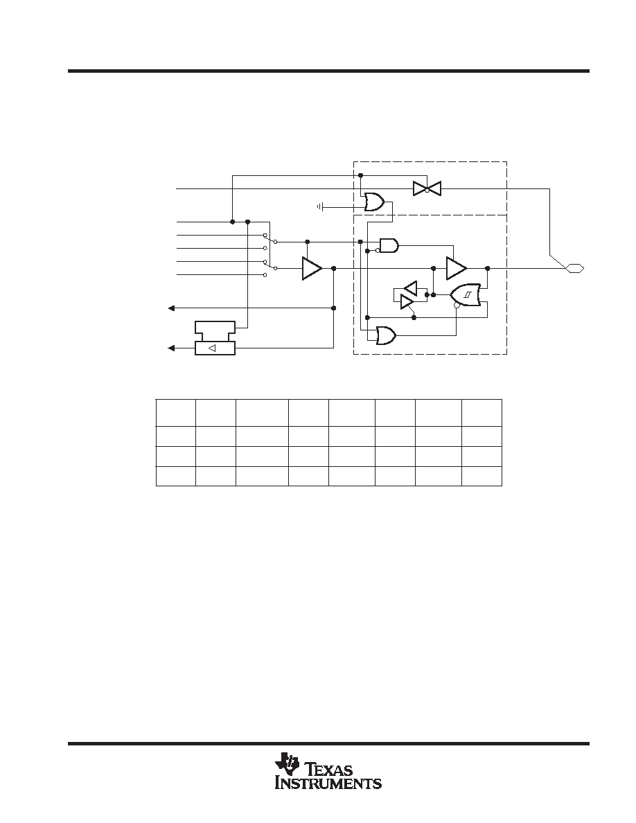
MSP430x41x
MIXED SIGNAL MICROCONTROLLER
SLAS340G - MAY 2001 - REVISED JUNE 2004
45
POST OFFICE BOX 655303
∑
DALLAS, TEXAS 75265
APPLICATION INFORMATION
input/output schematic (continued)
port P5, P5.5 to P5.7, input/output with Schmitt-trigger
P5SEL.5
P5DIR.5
P5OUT.5
P5IN.5
R13
P5DIR.5
DVSS
Unused
PnSEL.x
PnDIR.x
Direction
From Module
PnOUT.x
Module X
OUT
PnIN.x
Rxx
Module X IN
Control
NOTE: 5
x
7
DVSS
Unused
0: Port Active
1: Rxx Function
P5OUT.x
Module X OUT
P5DIR.x
Direction Control
From Module
P5SEL.x
D
EN
P5.x
0
1
1
0
Pad Logic
0: Input
1: Output
Bus
keeper
Module X IN
P5IN.x
Rxx
Active
P5.5/R13
P5.6/R23
DVSS
Unused
P5SEL.6
P5DIR.6
P5OUT.6
P5IN.6
R23
P5DIR.6
DVSS
Unused
P5SEL.7
P5DIR.7
P5OUT.7
P5IN.7
R33
P5DIR.7
DVSS
Unused
P5.7/R33
NOTE:
The direction control bits P5SEL.5, P5SEL.6, and P5SEL.7 are used to distinguish between port
and LCD analog level functions. Note that 4MUX and 3MUX LCDs require all Rxx signals R33 to
R03, a 2MUX LCD requires R33, R13, and R03, and a static LCD requires only R33 and R03.
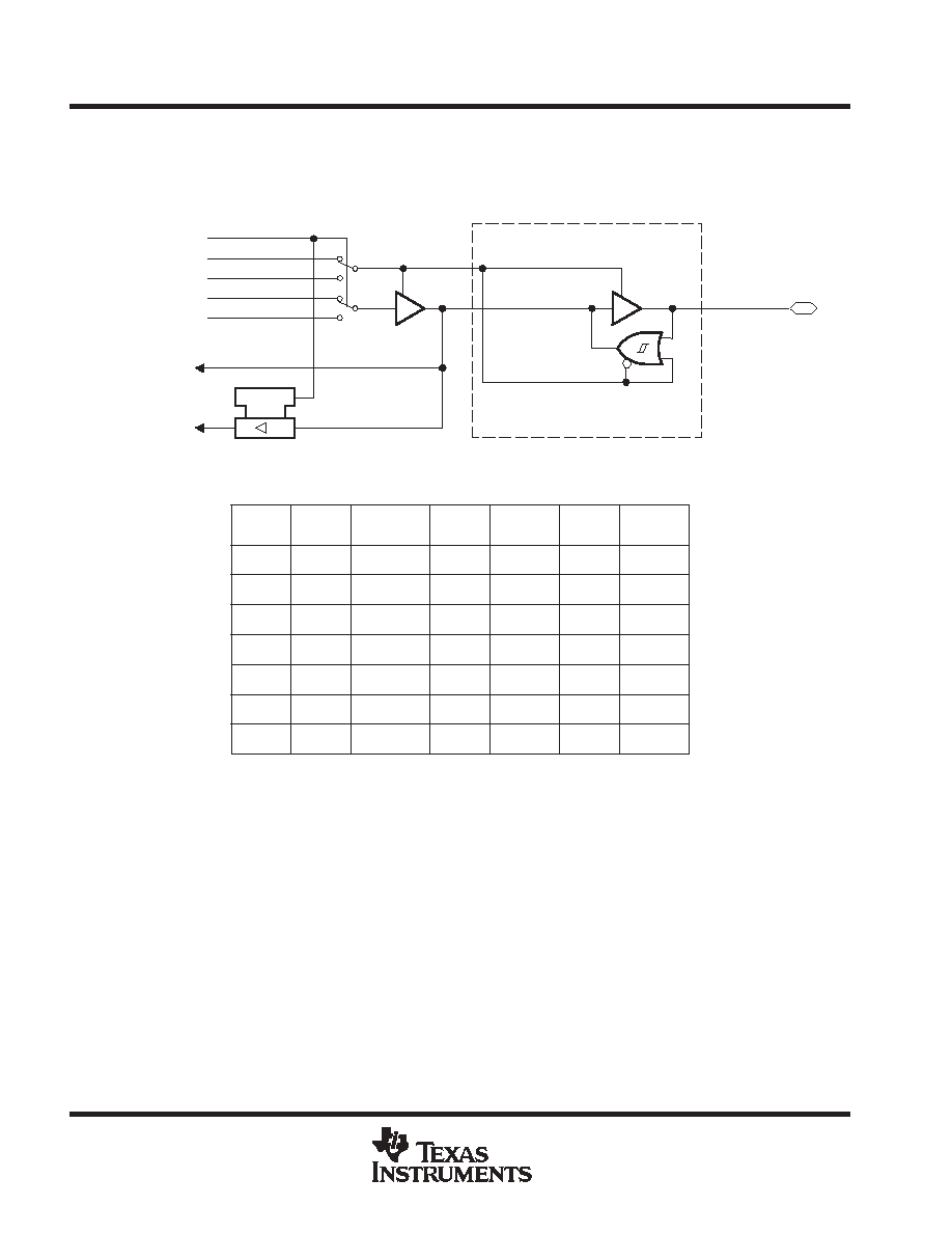
MSP430x41x
MIXED SIGNAL MICROCONTROLLER
SLAS340G - MAY 2001 - REVISED JUNE 2004
46
POST OFFICE BOX 655303
∑
DALLAS, TEXAS 75265
APPLICATION INFORMATION
input/output schematic (continued)
port P6, P6.0 to P6.6, input/output with Schmitt-trigger
P6OUT.x
Module X OUT
P6DIR.x
Direction Control
From Module
P6SEL.x
D
EN
P6.x
0
1
1
0
0: Input
1: Output
Module X IN
P6IN.x
P6.
P6.0
P6SEL.0
P6DIR.0
P6OUT.0
P6IN.0
DVSS
Unused
PnSEL.x
PnDIR.x
Direction
From Module
PnOUT.x
Module X
OUT
PnIN.x
Module X IN
Control
NOTE: 0
x
6
DVSS
DVSS
DVSS
DVSS
Unused
Unused
Unused
Unused
Unused
Unused
DVSS
DVSS
P6SEL.1
P6DIR.1
P6OUT.1
P6IN.1
P6SEL.2
P6DIR.2
P6OUT.2
P6IN.2
P6SEL.3
P6DIR.3
P6OUT.3
P6IN.3
P6SEL.4
P6DIR.4
P6OUT.4
P6IN.4
P6SEL.5
P6DIR.5
P6OUT.5
P6IN.5
P6SEL.6
P6DIR.6
P6OUT.6
P6IN.6
P6DIR.0
P6DIR.1
P6DIR.2
P6DIR.3
P6DIR.4
P6DIR.5
P6DIR.6
P6.
P6.1
P6.2
P6.
P6.4
P6.
P6.5
P6.
P6.6
P6.3
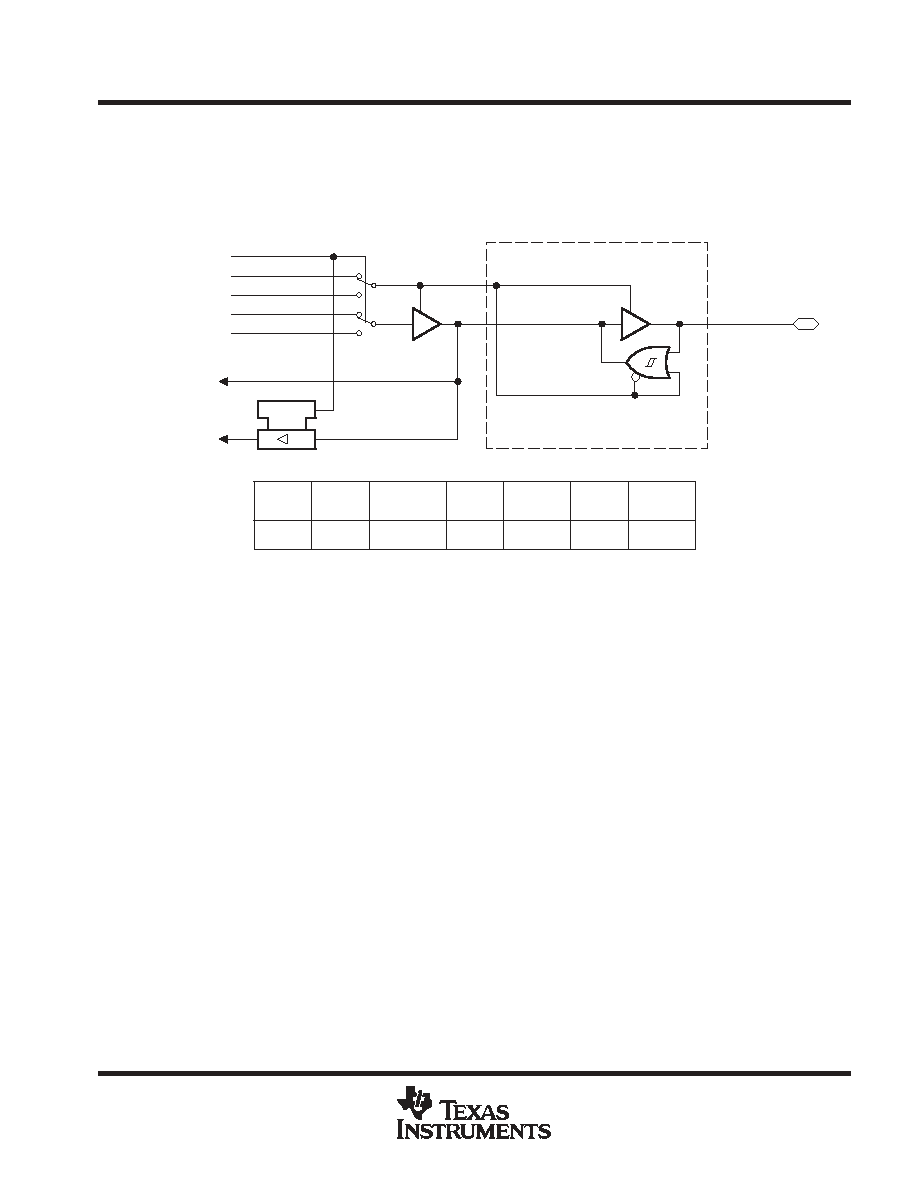
MSP430x41x
MIXED SIGNAL MICROCONTROLLER
SLAS340G - MAY 2001 - REVISED JUNE 2004
47
POST OFFICE BOX 655303
∑
DALLAS, TEXAS 75265
APPLICATION INFORMATION
input/output schematic (continued)
port P6, P6.7 input/output with Schmitt-trigger
MSP430x412/413 only
P6OUT.7
Module X OUT
P6DIR.7
Direction Control
From Module
P6SEL.7
D
EN
P6.x
0
1
1
0
0: Input
1: Output
Module X IN
P6IN.7
P6.7
PnSEL.x
PnDIR.x
Direction
From Module
PnOUT.x
Module X
OUT
PnIN.x
Module X IN
Control
DVSS
Unused
P6SEL.7
P6DIR.7
P6OUT.7
P6IN.7
P6DIR.7
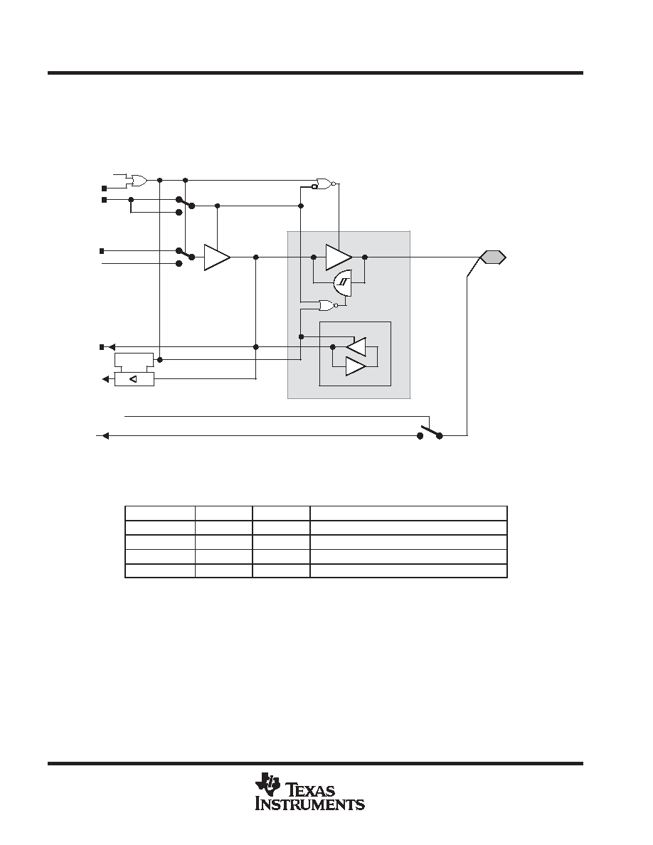
MSP430x41x
MIXED SIGNAL MICROCONTROLLER
SLAS340G - MAY 2001 - REVISED JUNE 2004
48
POST OFFICE BOX 655303
∑
DALLAS, TEXAS 75265
APPLICATION INFORMATION
input/output schematic (continued)
port P6, P6.7 input/output with Schmitt-trigger
MSP430F415/417 only
P6IN.7
Module X IN
Pad Logic
EN
D
P6OUT.7
P6DIR.7
P6SEL.7
DVss
0
1
0
1
Bus Keeper
To SVS
0: Input
1: Output
P6.7/SVSIN
SVS VLDx=15
1
SVS VLDx=15
NOTE: Analog signals applied to digital gates can cause current flow from the positive to the negative terminal. The throughput current flows if
the analog signal is in the range of transitions 0
1 or 1
0. The value of the throughput current depends on the driving capability of the
gate. For MSP430, it is approximately 100
µ
A.
Use P6SEL.x=1 to prevent throughput current. P6SEL.x should be set, if an analog signal is applied to the pin.
SVS VLDx = 15
P6SEL.7
P6DIR.7
Port Function
0
0
0
P6.7 Input
0
0
1
P6.7 Output
0
1
X
Undefined
1
X
X
SVSIN
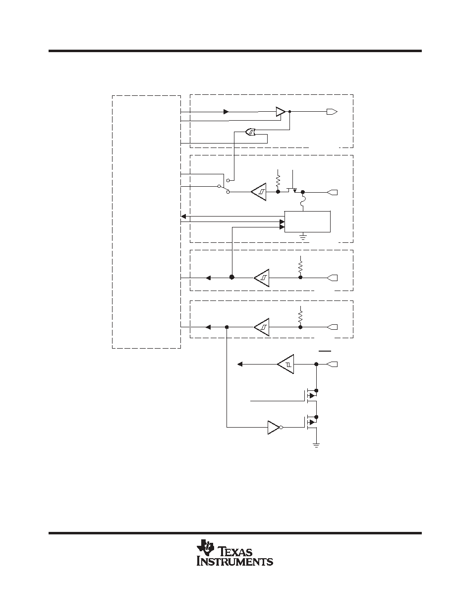
MSP430x41x
MIXED SIGNAL MICROCONTROLLER
SLAS340G - MAY 2001 - REVISED JUNE 2004
49
POST OFFICE BOX 655303
∑
DALLAS, TEXAS 75265
APPLICATION INFORMATION
JTAG pins TMS, TCK, TDI/TCLK, TDO/TDI, input/output with Schmitt-trigger or output
TDI
TDO
TMS
TDI/TCLK
TDO/TDI
Controlled
by JTAG
TCK
TMS
TCK
DVCC
Controlled by JTAG
Test
JTAG
and
Emulation
Module
DVCC
DVCC
Burn and Test
Fuse
G
D
S
U
G
D
S
U
TCK
Tau ~ 50 ns
Brownout
Controlled by JTAG
RST/NMI

MSP430x41x
MIXED SIGNAL MICROCONTROLLER
SLAS340G - MAY 2001 - REVISED JUNE 2004
50
POST OFFICE BOX 655303
∑
DALLAS, TEXAS 75265
APPLICATION INFORMATION
JTAG fuse check mode
MSP430 devices that have the fuse on the TDI/TCLK terminal have a fuse check mode that tests the continuity
of the fuse the first time the JTAG port is accessed after a power-on reset (POR). When activated, a fuse check
current, I
TF
, of 1.8 mA at 3 V can flow from the TDI/TCLK pin to ground if the fuse is not burned. Care must be
taken to avoid accidentally activating the fuse check mode and increasing overall system power consumption.
Activation of the fuse check mode occurs with the first negative edge on the TMS pin after power up or if the
TMS is being held low during power up. The second positive edge on the TMS pin deactivates the fuse check
mode. After deactivation, the fuse check mode remains inactive until another POR occurs. After each POR the
fuse check mode has the potential to be activated.
The fuse check current only flows when the fuse check mode is active and the TMS pin is in a low state (see
Figure 22). Therefore, the additional current flow can be prevented by holding the TMS pin high (default
condition).
The JTAG pins are terminated internally, and therefore do not require external termination.
Time TMS Goes Low After POR
TMS
ITF
ITDI/TCLK
Figure 22. Fuse Check Mode Current, MSP430C41x, MSP430F41x
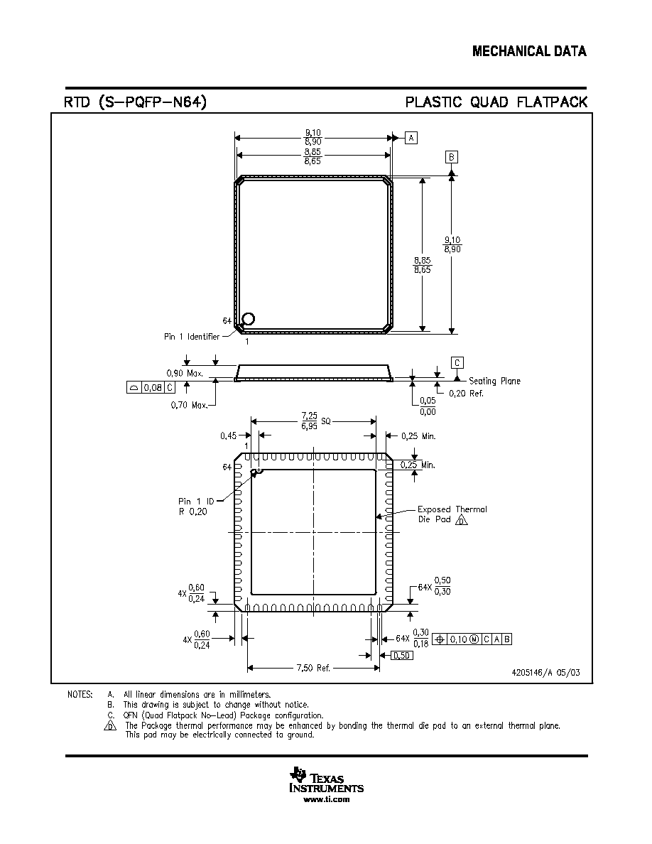
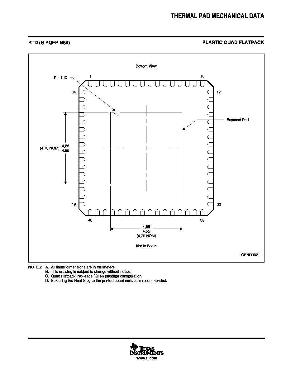

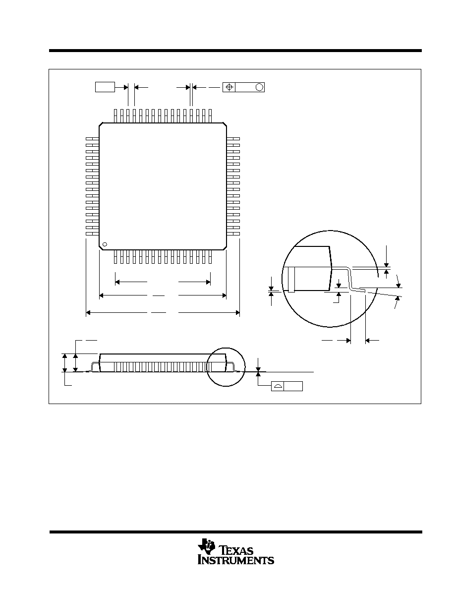
MECHANICAL DATA
MTQF008A ≠ JANUARY 1995 ≠ REVISED DECEMBER 1996
1
POST OFFICE BOX 655303
∑
DALLAS, TEXAS 75265
PM (S-PQFP-G64)
PLASTIC QUAD FLATPACK
4040152 / C 11/96
32
17
0,13 NOM
0,25
0,45
0,75
Seating Plane
0,05 MIN
Gage Plane
0,27
33
16
48
1
0,17
49
64
SQ
SQ
10,20
11,80
12,20
9,80
7,50 TYP
1,60 MAX
1,45
1,35
0,08
0,50
M
0,08
0
∞
≠ 7
∞
NOTES: A. All linear dimensions are in millimeters.
B. This drawing is subject to change without notice.
C. Falls within JEDEC MS-026
D. May also be thermally enhanced plastic with leads connected to the die pads.

IMPORTANT NOTICE
Texas Instruments Incorporated and its subsidiaries (TI) reserve the right to make corrections, modifications,
enhancements, improvements, and other changes to its products and services at any time and to discontinue
any product or service without notice. Customers should obtain the latest relevant information before placing
orders and should verify that such information is current and complete. All products are sold subject to TI's terms
and conditions of sale supplied at the time of order acknowledgment.
TI warrants performance of its hardware products to the specifications applicable at the time of sale in
accordance with TI's standard warranty. Testing and other quality control techniques are used to the extent TI
deems necessary to support this warranty. Except where mandated by government requirements, testing of all
parameters of each product is not necessarily performed.
TI assumes no liability for applications assistance or customer product design. Customers are responsible for
their products and applications using TI components. To minimize the risks associated with customer products
and applications, customers should provide adequate design and operating safeguards.
TI does not warrant or represent that any license, either express or implied, is granted under any TI patent right,
copyright, mask work right, or other TI intellectual property right relating to any combination, machine, or process
in which TI products or services are used. Information published by TI regarding third-party products or services
does not constitute a license from TI to use such products or services or a warranty or endorsement thereof.
Use of such information may require a license from a third party under the patents or other intellectual property
of the third party, or a license from TI under the patents or other intellectual property of TI.
Reproduction of information in TI data books or data sheets is permissible only if reproduction is without
alteration and is accompanied by all associated warranties, conditions, limitations, and notices. Reproduction
of this information with alteration is an unfair and deceptive business practice. TI is not responsible or liable for
such altered documentation.
Resale of TI products or services with statements different from or beyond the parameters stated by TI for that
product or service voids all express and any implied warranties for the associated TI product or service and
is an unfair and deceptive business practice. TI is not responsible or liable for any such statements.
Following are URLs where you can obtain information on other Texas Instruments products and application
solutions:
Products
Applications
Amplifiers
amplifier.ti.com
Audio
www.ti.com/audio
Data Converters
dataconverter.ti.com
Automotive
www.ti.com/automotive
DSP
dsp.ti.com
Broadband
www.ti.com/broadband
Interface
interface.ti.com
Digital Control
www.ti.com/digitalcontrol
Logic
logic.ti.com
Military
www.ti.com/military
Power Mgmt
power.ti.com
Optical Networking
www.ti.com/opticalnetwork
Microcontrollers
microcontroller.ti.com
Security
www.ti.com/security
Telephony
www.ti.com/telephony
Video & Imaging
www.ti.com/video
Wireless
www.ti.com/wireless
Mailing Address:
Texas Instruments
Post Office Box 655303 Dallas, Texas 75265
Copyright
2004, Texas Instruments Incorporated