 | –≠–ª–µ–∫—Ç—Ä–æ–Ω–Ω—ã–π –∫–æ–º–ø–æ–Ω–µ–Ω—Ç: N8T14 | –°–∫–∞—á–∞—Ç—å:  PDF PDF  ZIP ZIP |
N8T14, SN55122, SN75122
TRIPLE LINE RECEIVERS
SLLS075B ≠ D1334, SEPTEMBER 1973 ≠ REVISED FEBRUARY 1993
POST OFFICE BOX 655303
∑
DALLAS, TEXAS 75265
Copyright
©
1993, Texas Instruments Incorporated
2≠1
∑
Designed for Digital Data Transmission
Over Coaxial Cable, Strip Line, or Twisted
Pair
∑
Designed for Operation With 50-
to 500-
Transmission Lines
∑
TTL Compatible
∑
Single 5-V Supply
∑
Built-Input Threshold Hysteresis
∑
High-Speed . . . Typical Propagation Delay
Time = 20 ns
∑
Independent Channel Strobes
∑
Input Gating Increases Application
Flexibility
∑
Fanout to 10 Series 54/74 Standard Loads
∑
Can Be Used With Dual Line Drivers
SN55121 and SN75121
∑
Interchangeable With Signetics N8T14
description
The N8T14, SN55122, and SN75122 are triple
line receivers that are designed for digital data
transmission over lines having impedances from
50
to 500
. They are also compatible with
standard TTL-logic and supply voltage levels.
The N8T14, SN55122, and SN75122 have receiver inputs with built-in hysteresis to provide increased noise
margin for single-ended systems. The high impedance of this input presents a minimum load to the driver and
allows termination of the transmission line in its characteristic impedance to minimize line reflection. An open
line will affect the receiver input as would a low-level voltage. The receiver can withstand a level of ≠ 0.15 V with
power on or off. The other inputs are in TTL configuration. The S input must be high to enable the receiver input.
Two of the line receivers have A and B inputs that, if both are high, will hold the output low. The third receiver
has only an A input that, if high, will hold the output low.
The SN55122 is characterized for operation over the full military temperature range of ≠ 55
∞
C to 125
∞
C. The
N8T14 and SN75122 are characterized for operation from 0
∞
C to 70
∞
C.
3
2
1 20 19
9 10 11 12 13
4
5
6
7
8
18
17
16
15
14
1R
1Y
NC
3A
3S
2R
2S
NC
2A
2B
SN55122 . . . FK PACKAGE
(TOP VIEW)
1B
1A
NC
3Y
3R
1S
2Y
GND
NC
NC ≠ No internal connection
1
2
3
4
5
6
7
8
16
15
14
13
12
11
10
9
1A
1B
2R
2S
2A
2B
2Y
GND
V
CC
1S
1R
1Y
3A
3S
3R
3Y
SN55122 . . . J PACKAGE
N8T14, SN75122 . . . D OR N PACKAGE
(TOP VIEW)
CC
V
THE N8T14 AND SN75122 ARE NOT
RECOMMENDED FOR NEW DESIGN
PRODUCTION DATA information is current as of publication date.
Products conform to specifications per the terms of Texas Instruments
standard warranty. Production processing does not necessarily include
testing of all parameters.
N8T14, SN55122, SN75122
TRIPLE LINE RECEIVERS
SLLS075B ≠ D1334, SEPTEMBER 1973 ≠ REVISED FEBRUARY 1993
POST OFFICE BOX 655303
∑
DALLAS, TEXAS 75265
2≠2
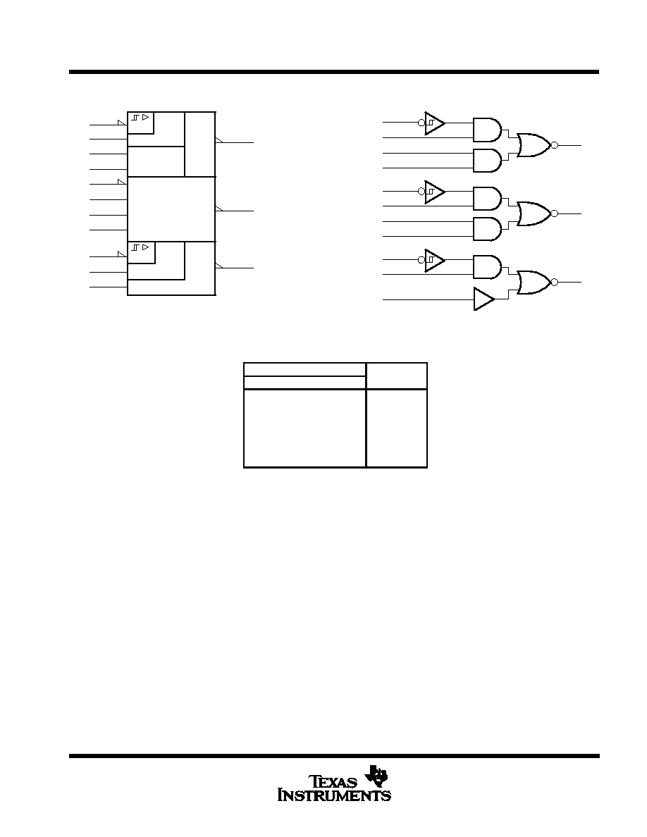
logic symbol
logic diagram
3A
3S
3R
2B
2A
2S
2R
1B
1A
1S
1R
9
7
13
1Y
2Y
3Y
12
11
10
6
5
4
3
2
1
15
14
2Y
15
12
11
10
6
5
4
3
2
1
14
3Y
1Y
9
7
13
3A
3S
3R
2B
2A
2S
2R
1B
1A
1S
1R
1
&
&
&
This symbol is in accordance with ANSI/IEEE Std 91-1984
and IEC Publication 617-12.
Pin numbers shown are for the D, J, and N packages.
1
FUNCTION TABLE
INPUTS
OUTPUT
A
B
R
S
Y
H
H
X
X
L
X
X
L
H
L
L
X
H
X
H
L
X
X
L
H
X
L
H
X
H
X
L
X
L
H
B input and last two lines of the function table are
applicable to receivers 1 and 2 only.
H = high level, L = low level, X = irrelevant

N8T14, SN55122, SN75122
TRIPLE LINE RECEIVERS
SLLS075B ≠ D1334, SEPTEMBER 1973 ≠ REVISED FEBRUARY 1993
POST OFFICE BOX 655303
∑
DALLAS, TEXAS 75265
2≠3
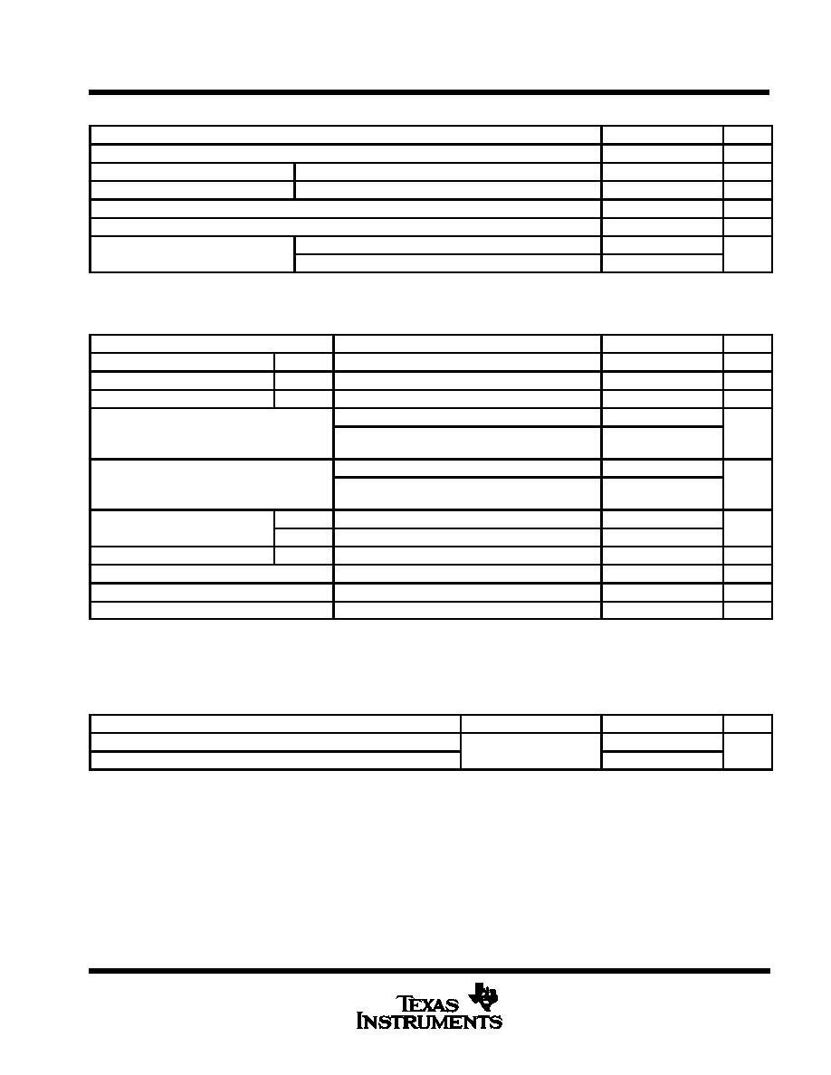
schematic diagram (each receiver)
58
13, 7, 9
Y
800
4 k
4 k
A
B
V
S
VCC
To Other
Receivers
R
V
GND
. . . VCC bus
V
To Other
Receiver
V
B input is provided on receivers 1 and 2 only.
Resistor values shown are nominal.
absolute maximum ratings over operating free-air temperature range (unless otherwise noted)
Supply voltage, V
CC
(see Note 1)
6 V
. . . . . . . . . . . . . . . . . . . . . . . . . . . . . . . . . . . . . . . . . . . . . . . . . . . . . . . . . . . . .
Input voltage:
R input
6 V
. . . . . . . . . . . . . . . . . . . . . . . . . . . . . . . . . . . . . . . . . . . . . . . . . . . . . . . . . . . . . . . . . . . . .
A, B, or S input
5.5 V
. . . . . . . . . . . . . . . . . . . . . . . . . . . . . . . . . . . . . . . . . . . . . . . . . . . . . . . . . . . .
Output voltage
6 V
. . . . . . . . . . . . . . . . . . . . . . . . . . . . . . . . . . . . . . . . . . . . . . . . . . . . . . . . . . . . . . . . . . . . . . . . . . . . .
Output current
±
100 mA
. . . . . . . . . . . . . . . . . . . . . . . . . . . . . . . . . . . . . . . . . . . . . . . . . . . . . . . . . . . . . . . . . . . . . . . .
Continuous total power dissipation (see Note 2)
See Dissipation Rating Table
. . . . . . . . . . . . . . . . . . . . . . . . .
Operating free-air temperature range:
SN55122
≠ 55
∞
C to 125
∞
C
. . . . . . . . . . . . . . . . . . . . . . . . . . . . . . . . . .
N8T14, SN75122
0
∞
C to 70
∞
C
. . . . . . . . . . . . . . . . . . . . . . . . . . . . . . .
Storage temperature range
≠ 65
∞
C to 150
∞
C
. . . . . . . . . . . . . . . . . . . . . . . . . . . . . . . . . . . . . . . . . . . . . . . . . . . . . . .
Case temperature for 60 seconds: FK package
260
∞
C
. . . . . . . . . . . . . . . . . . . . . . . . . . . . . . . . . . . . . . . . . . . . . .
Lead temperature 1,6 mm (1/16 inch) from case for 60 seconds: J package
300
∞
C
. . . . . . . . . . . . . . . . . . . . .
Lead temperature 1,6 mm (1/16 inch) from case for 10 seconds: D or N package
260
∞
C
. . . . . . . . . . . . . . . .
NOTES: 1. Voltage values are with respect to network ground terminal.
2. The SN55122 chips are alloy mounted, and the SN75122 chips are glass mounted.
DISSIPATION RATING TABLE
PACKAGE
TA
25
∞
C
POWER RATING
DERATING FACTOR
ABOVE TA = 25
∞
C
TA = 70
∞
C
POWER RATING
TA = 125
∞
C
POWER RATING
D
950 mW
7.6 mW/
∞
C
608 mW
≠
FK
1375 mW
11.0 mW/
∞
C
880 mW
275 mW
J
1375 mW
11.0 mW/
∞
C
880 mW
275 mW
N
1150 mW
9.2 mW/
∞
C
736 mW
≠
N8T14, SN55122, SN75122
TRIPLE LINE RECEIVERS
SLLS075B ≠ D1334, SEPTEMBER 1973 ≠ REVISED FEBRUARY 1993
POST OFFICE BOX 655303
∑
DALLAS, TEXAS 75265
2≠4
recommended operating conditions
MIN
NOM
MAX
UNIT
Supply voltage, VCC
4.75
5
5.25
V
High-level input voltage, VIH
A, B, R, or S
2
V
Low-level input voltage, VIL
A, B, R, or S
0.8
V
High-level output current, IOH
≠ 500
µ
A
Low-level output current, IOL
16
mA
Operating free air temperature TA
SN55122
≠ 55
125
∞
C
Operating free-air temperature, TA
SN75122
0
70
∞
C
electrical characteristics over recommended operating free-air temperature, V
CC
= 4.75 V to
5.25 V (unless otherwise noted)
PARAMETER
TEST CONDITIONS
MIN
TYP
MAX
UNIT
Vhys
Hysteresis (VT+ ≠ VT≠)
R
VCC = 5 V,
TA = 25
∞
C,
See Figures 2 and 4
0.3
0.6
V
VIK
Input clamp voltage
A, B, or S
VCC = 5 V,
II = ≠12 mA
≠1.5
V
VI(BR)
Input breakdown voltage
A, B, or S
VCC = 5 V,
II = 10 mA
5.5
V
VIH = 2 V,
VIL = 0.8 V,
IOH = ≠ 500
µ
A
2.6
VOH
High-level output voltage
VI(A) = 0,
VI(B) = 0,
VI(S) = 2 V,
VI(R) = 1.45 V, IOH = ≠ 500
µ
A, See Note 3
2.6
V
VIH = 2 V,
VIL = 0.8 V,
IOL = 16 mA
0.4
VOL
Low-level output voltage
VI(A) = 0,
VI(B) = 0,
VI(S) = 2 V,
VI(R) = 1.45 V, IOL = 16 mA,
See Note 4
0.4
V
IIH
High level input current
A, B, or S
VI = 4.5 V
40
µ
A
IIH
High-level input current
R
VI = 3.8 V
170
µ
A
IIL
Low-level input current
A, B, or S
VI = 0.4 V,
VIR = 0.8 V
≠ 0.1
≠1.6
mA
IOS
Short-circuit output current
VCC = 5 V,
TA = 25
∞
C
≠ 50
≠100
mA
ICCH
High-level supply current
VCC = MAX,
All inputs at 0.8 V,
Outputs open
72
mA
ICCL
Low-level supply current
VCC = MAX,
All inputs at 2 V,
Outputs open
100
mA
All typical values are at VCC = 5 V and TA = 25
∞
C.
Not more than one output should be shorted at a time, and duration of the short circuit should not exceed one second.
NOTES: 3. The receiver input is high immediately before being reduced to 1.45 V.
4. The receiver input is low immediately before being increased to 1.45 V.
switching characteristics, V
CC
= 5 V, T
A
= 25
∞
C
PARAMETER
TEST CONDITIONS
MIN
TYP
MAX
UNIT
tPLH
Propagation delay time, low-to-high-level output from R input
See Figure 1
20
30
ns
tPHL
Propagation delay time, high-to-low-level output from R input
See Figure 1
20
30
ns
N8T14, SN55122, SN75122
TRIPLE LINE RECEIVERS
SLLS075B ≠ D1334, SEPTEMBER 1973 ≠ REVISED FEBRUARY 1993
POST OFFICE BOX 655303
∑
DALLAS, TEXAS 75265
2≠5
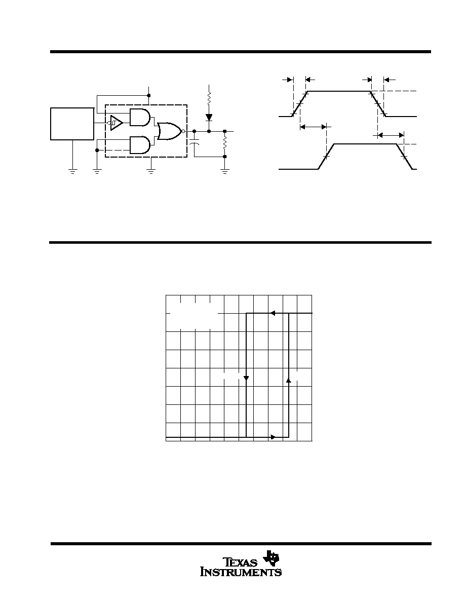
PARAMETER MEASUREMENT INFORMATION
VCC
2.6 V
84.5
1N3064
Output
5 k
CL =
30 pF
(see Note B)
TEST CIRCUIT
Pulse
Generator
(see Note A)
5 ns
90%
1.5 V
Input
10%
0 V
2.6 V
VOH
Output
VOL
tPHL
tPLH
VOLTAGE WAVEFORMS
5 ns
90%
1.5 V
10%
1.5 V
1.5 V
NOTES: A. The pulse generator has the following characteristics: ZO = 50
, tw = 200 ns, duty cycle = 50%, PRR
500 kHz.
B. CL includes probe and jig capacitance.
Figure 1. Test Circuit and Voltage Waveforms
TYPICAL CHARACTERISTICS
2
1.5
0.5
0
0
0.4
0.8
1
VO ≠ Output V
oltage ≠ V
2.5
3.5
VI ≠ Input Voltage ≠ V
OUTPUT VOLTAGE
vs
INPUT VOLTAGE
4
1.4
1.8
2
1
3
V
O
VI
VT ≠
VT +
VCC = 5 V
No Load
TA = 25
_
C
Figure 2

N8T14, SN55122, SN75122
TRIPLE LINE RECEIVERS
SLLS075B ≠ D1334, SEPTEMBER 1973 ≠ REVISED FEBRUARY 1993
POST OFFICE BOX 655303
∑
DALLAS, TEXAS 75265
2≠6
APPLICATION INFORMATION
75-
Coaxial Cable
1/3 SN55122
1/3 SN55122
1/3 SN55122
1/2 SN55121
1/2 SN55121
1/2 SN55121
75-
Coaxial Cable
75-
Coaxial
Cable
1/2 SN55121
75
75
75
75
Figure 3. Single-Ended Party Line Circuits
R
Input
VT +
VT ≠
VIH
VIL
VOH
VOL
Output
NOTE: The high gain and built-in hysteresis of the SN55122 and
SN75122 line receivers enable them to be used as Schmitt
triggers in squaring pulses.
Figure 4. Pulse Squaring

IMPORTANT NOTICE
Texas Instruments (TI) reserves the right to make changes to its products or to discontinue any semiconductor
product or service without notice, and advises its customers to obtain the latest version of relevant information
to verify, before placing orders, that the information being relied on is current and complete.
TI warrants performance of its semiconductor products and related software to the specifications applicable at
the time of sale in accordance with TI's standard warranty. Testing and other quality control techniques are
utilized to the extent TI deems necessary to support this warranty. Specific testing of all parameters of each
device is not necessarily performed, except those mandated by government requirements.
Certain applications using semiconductor products may involve potential risks of death, personal injury, or
severe property or environmental damage ("Critical Applications").
TI SEMICONDUCTOR PRODUCTS ARE NOT DESIGNED, INTENDED, AUTHORIZED, OR WARRANTED
TO BE SUITABLE FOR USE IN LIFE-SUPPORT APPLICATIONS, DEVICES OR SYSTEMS OR OTHER
CRITICAL APPLICATIONS.
Inclusion of TI products in such applications is understood to be fully at the risk of the customer. Use of TI
products in such applications requires the written approval of an appropriate TI officer. Questions concerning
potential risk applications should be directed to TI through a local SC sales office.
In order to minimize risks associated with the customer's applications, adequate design and operating
safeguards should be provided by the customer to minimize inherent or procedural hazards.
TI assumes no liability for applications assistance, customer product design, software performance, or
infringement of patents or services described herein. Nor does TI warrant or represent that any license, either
express or implied, is granted under any patent right, copyright, mask work right, or other intellectual property
right of TI covering or relating to any combination, machine, or process in which such semiconductor products
or services might be or are used.
Copyright
©
1998, Texas Instruments Incorporated