 | –≠–ª–µ–∫—Ç—Ä–æ–Ω–Ω—ã–π –∫–æ–º–ø–æ–Ω–µ–Ω—Ç: NE5534AFK | –°–∫–∞—á–∞—Ç—å:  PDF PDF  ZIP ZIP |
NE5534, NE5534A, SA5534. SA5534A
LOW NOISE OPERATIONAL AMPLIFIERS
SLOS070C - JULY 1979 - REVISED SEPTEMBER 2004
1
POST OFFICE BOX 655303
∑
DALLAS, TEXAS 75265
D
Equivalent Input Noise Voltage . . .
3.5 nV/
/
Hz Typ
D
Unity-Gain Bandwidth . . . 10 MHz Typ
D
Common-Mode Rejection Ratio . . .
100 dB Typ
D
High DC Voltage Gain . . . 100 V/mV Typ
D
Peak-to-Peak Output Voltage Swing
32 V Typ With V
CC
+
=
+
18 V and R
L
= 600
W
D
High Slew Rate . . . 13 V/
m
s Typ
D
Wide Supply-Voltage Range
+
3 V to
+
20 V
D
Low Harmonic Distortion
D
Offset Nulling Capability
D
External Compensation Capability
description/ordering information
The NE5534, NE5534A, SA5534, and SA5534A are high-performance operational amplifiers combining
excellent dc and ac characteristics. Some of the features include very low noise, high output-drive capability,
high unity-gain and maximum-output-swing bandwidths, low distortion, and high slew rate.
These operational amplifiers are compensated internally for a gain equal to or greater than three. Optimization
of the frequency response for various applications can be obtained by use of an external compensation
capacitor between COMP and COMP/BAL. The devices feature input-protection diodes, output short-circuit
protection, and offset-voltage nulling capability with use of the BALANCE and COMP/BAL pins (see the
application circuit diagram).
For the NE5534A and SA5534A, a maximum limit is specified for the equivalent input noise voltage.
Please be aware that an important notice concerning availability, standard warranty, and use in critical applications of
Texas Instruments semiconductor products and disclaimers thereto appears at the end of this data sheet.
Copyright
2004, Texas Instruments Incorporated
PRODUCTION DATA information is current as of publication date.
Products conform to specifications per the terms of Texas Instruments
standard warranty. Production processing does not necessarily include
testing of all parameters.
1
2
3
4
8
7
6
5
BALANCE
IN-
IN+
V
CC-
COMP/BAL
V
CC+
OUT
COMP
NE5534, SA5534 . . . D (SOIC), P (PDIP),
OR PS (SOP) PACKAGE
NE5534A, SA5534A . . . D (SOIC) OR P (PDIP) PACKAGE
(TOP VIEW)
NE5534, NE5534A, SA5534. SA5534A
LOW NOISE OPERATIONAL AMPLIFIERS
SLOS070C - JULY 1979 - REVISED SEPTEMBER 2004
2
POST OFFICE BOX 655303
∑
DALLAS, TEXAS 75265
description/ordering information (continued)
ORDERING INFORMATION
TA
VIOmax
AT 25
∞
C
PACKAGE
ORDERABLE
PART NUMBER
TOP-SIDE
MARKING
PDIP (P)
Tube of 50
NE5534P
NE5534P
PDIP (P)
Tube of 50
NE5534AP
NE5534AP
Tube of 75
NE5534D
NE5534
0
∞
C to 70
∞
C
4 mV
SOIC (D)
Reel of 2500
NE5534DR
NE5534
0 C to 70 C
4 mV
SOIC (D)
Tube of 75
NE5534AD
5534A
Reel of 2500
NE5534ADR
5534A
SOP (PS)
Reel of 2000
NE5534PSR
N5534
PDIP (P)
Tube of 50
SA5534P
SA5534P
PDIP (P)
Tube of 50
SA5534AP
SA5534AP
Tube of 75
SA5534D
SA5534
-40
∞
C to 85
∞
C
4 mV
SOIC (D)
Reel of 2500
SA5534DR
SA5534
-40
∞
C to 85
∞
C
4 mV
SOIC (D)
Tube of 75
SA5534AD
SA5534A
Reel of 2500
SA5534ADR
SA5534A
SOP (PS)
Tube of 80
SA553APS
SA5534
SOP (PS)
Reel of 2000
SA553APSR
SA5534
Package drawings, standard packing quantities, thermal data, symbolization, and PCB design guidelines are available
at www.ti.com/sc/package.
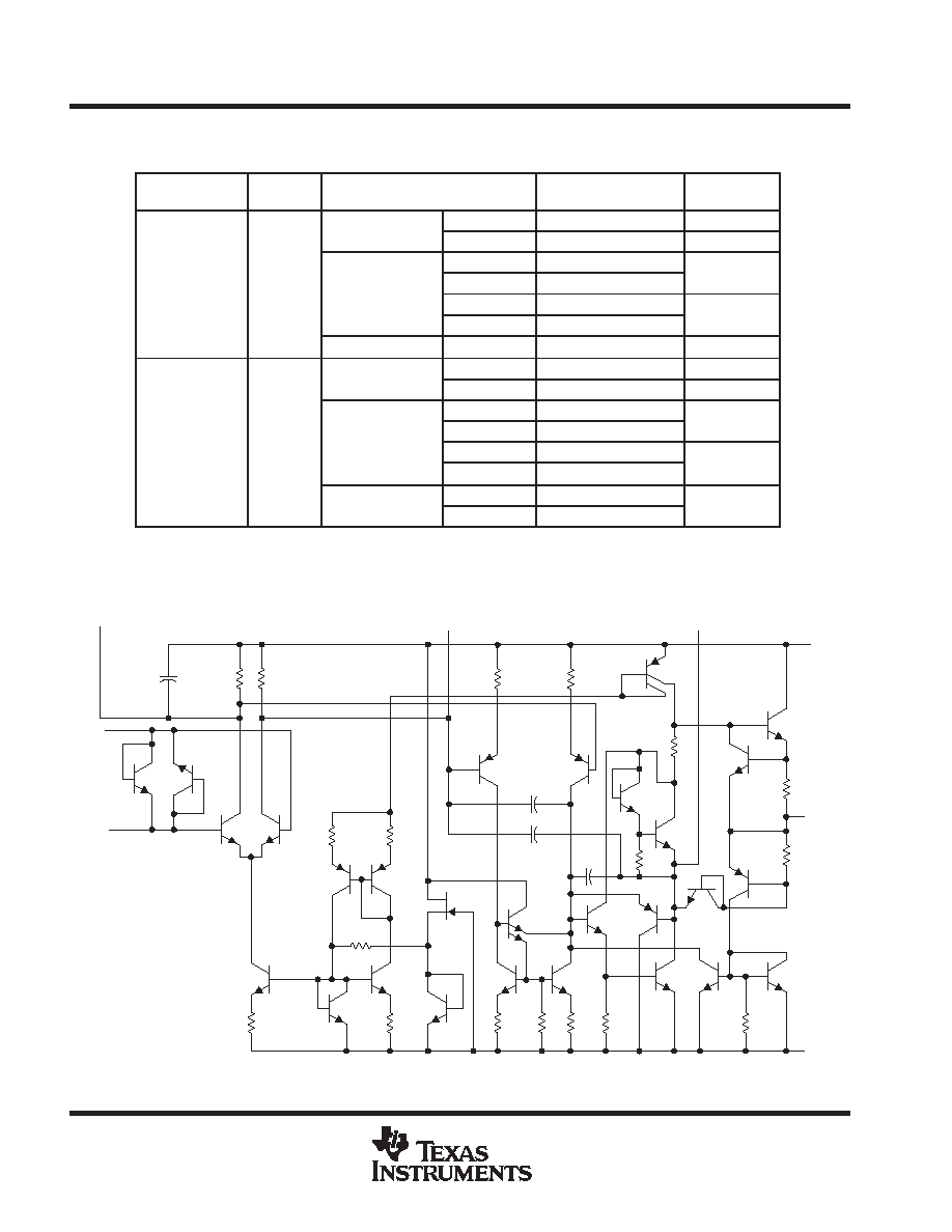
schematic
VCC-
OUT
15
15
12 k
12 k
7 pF
12 pF
40 pF
100 pF
IN+
IN-
BALANCE
COMP
COMP/BAL
8
5
7
4
6
2
3
1
All component values shown are nominal.
VCC+
NE5534, NE5534A, SA5534. SA5534A
LOW NOISE OPERATIONAL AMPLIFIERS
SLOS070C - JULY 1979 - REVISED SEPTEMBER 2004
3
POST OFFICE BOX 655303
∑
DALLAS, TEXAS 75265
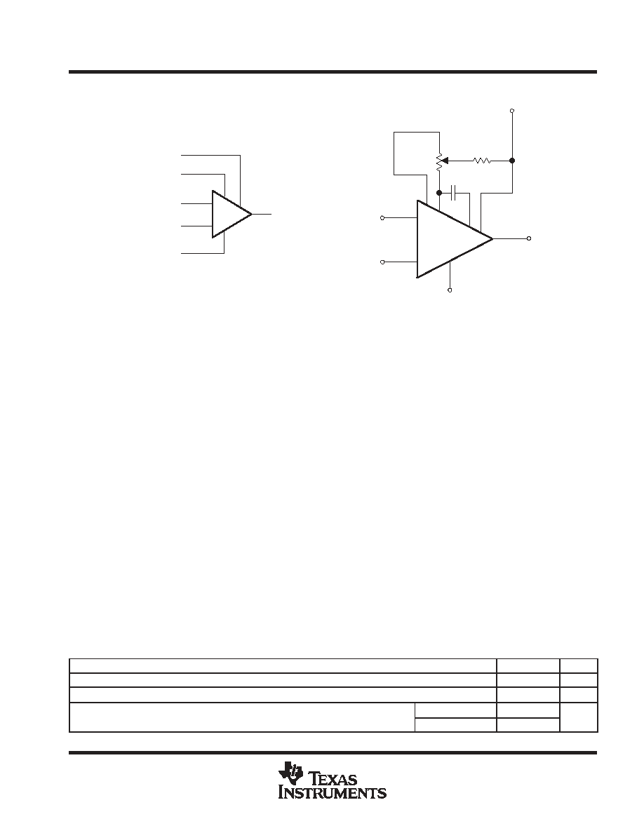
symbol
IN-
COMP/BAL
COMP
OUT
BALANCE
-
+
IN+
application circuit
-
+
22 k
100 k
7
2
3
VCC-
4
6
5
8
VCC+
1
CC
5534
Frequency Compensation and Offset-Voltage Nulling Circuit
absolute maximum ratings over operating free-air temperature range (unless otherwise noted)
Supply voltage: V
CC+
(see Note 1)
22 V
. . . . . . . . . . . . . . . . . . . . . . . . . . . . . . . . . . . . . . . . . . . . . . . . . . . . . . . . . . .
V
CC-
(see Note 1)
-22 V
. . . . . . . . . . . . . . . . . . . . . . . . . . . . . . . . . . . . . . . . . . . . . . . . . . . . . . . . . .
Input voltage either input (see Notes 1 and 2)
V
CC+
. . . . . . . . . . . . . . . . . . . . . . . . . . . . . . . . . . . . . . . . . . . . . . . . .
Input current (see Note 3)
±
10 mA
. . . . . . . . . . . . . . . . . . . . . . . . . . . . . . . . . . . . . . . . . . . . . . . . . . . . . . . . . . . . . . . .
Duration of output short circuit (see Note 4)
Unlimited
. . . . . . . . . . . . . . . . . . . . . . . . . . . . . . . . . . . . . . . . . . . . . . .
Package thermal impedance,
JA
(see Notes 5 and 6): D package
97
∞
C/W
. . . . . . . . . . . . . . . . . . . . . . . . . . . .
P package
85
∞
C/W
. . . . . . . . . . . . . . . . . . . . . . . . . . . .
PS package
95
∞
C/W
. . . . . . . . . . . . . . . . . . . . . . . . . . .
Operating virtual junction temperature, T
J
150
∞
C
. . . . . . . . . . . . . . . . . . . . . . . . . . . . . . . . . . . . . . . . . . . . . . . . . . .
Storage temperature range, T
stg
-65
∞
C to 150
∞
C
. . . . . . . . . . . . . . . . . . . . . . . . . . . . . . . . . . . . . . . . . . . . . . . . . . .
Stresses beyond those listed under "absolute maximum ratings" may cause permanent damage to the device. These are stress ratings only, and
functional operation of the device at these or any other conditions beyond those indicated under "recommended operating conditions" is not
implied. Exposure to absolute-maximum-rated conditions for extended periods may affect device reliability.
NOTES:
1. All voltage values, except differential voltages, are with respect to the midpoint between VCC+ and VCC-.
2. The magnitude of the input voltage must never exceed the magnitude of the supply voltage.
3. Excessive current will flow if a differential input voltage in excess of approximately 0.6 V is applied between the inputs, unless some
limiting resistance is used.
4. The output may be shorted to ground or to either power supply. Temperature and/or supply voltages must be limited to ensure the
maximum dissipation rating is not exceeded.
5. Maximum power dissipation is a function of TJ(max),
JA, and TA. The maximum allowable power dissipation at any allowable
ambient temperature is PD = (TJ(max) - TA)/
JA. Operating at the absolute maximum TJ of 150
∞
C can affect reliability.
6. The package thermal impedance is calculated in accordance with JESD 51-7.
recommended operating conditions
MIN
MAX
UNIT
VCC+
Supply voltage
5
15
V
VCC-
Supply voltage
-5
-15
V
TA
Operating free-air temperature range
NE5534, NE5534A
0
70
∞
C
TA
Operating free-air temperature range
SA5534, SA5534A
-40
85
∞
C
NE5534, NE5534A, SA5534. SA5534A
LOW NOISE OPERATIONAL AMPLIFIERS
SLOS070C - JULY 1979 - REVISED SEPTEMBER 2004
4
POST OFFICE BOX 655303
∑
DALLAS, TEXAS 75265
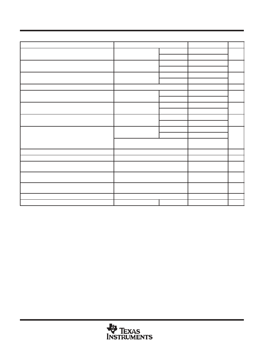
electrical characteristics, V
CC
±
=
±
15 V, T
A
= 25
∞
C (unless otherwise noted)
PARAMETER
TEST CONDITIONS
MIN
TYP
MAX
UNIT
VIO
Input offset voltage
VO = 0,
TA = 25
∞
C
0.5
4
mV
VIO
Input offset voltage
VO = 0,
RS = 50
TA = Full range
5
mV
IIO
Input offset current
VO = 0
TA = 25
∞
C
20
300
nA
IIO
Input offset current
VO = 0
TA = Full range
400
nA
IIB
Input bias current
VO = 0
TA = 25
∞
C
500
1500
nA
IIB
Input bias current
VO = 0
TA = Full range
2000
nA
VICR
Common-mode input voltage range
±
12
±
13
V
VO(PP) Maximum peak-to-peak output voltage swing
RL
600
VCC
±
=
±
15 V
24
26
V
VO(PP) Maximum peak-to-peak output voltage swing
RL
600
VCC
±
=
±
18 V
30
32
V
AVD
Large-signal differential voltage amplification
VO =
±
10 V,
TA = 25
∞
C
25
100
V/mV
AVD
Large-signal differential voltage amplification
VO =
±
10 V,
RL
600
TA = Full range
15
V/mV
Avd
Small-signal differential voltage amplification
f = 10 kHz
CC = 0
6
V/mV
Avd
Small-signal differential voltage amplification
f = 10 kHz
CC = 22 pF
2.2
V/mV
VO =
±
10 V
CC = 0
200
BOM
Maximum-output-swing bandwidth
VO =
±
10 V
CC = 22 pF
95
kHz
BOM
Maximum-output-swing bandwidth
VCC
±
=
±
18 V,
RL
600
,
VO =
±
14 V,
CC = 22 pF
70
kHz
B1
Unity-gain bandwidth
CC = 22 pF,
CL = 100 pF
10
MHz
ri
Input resistance
30
100
k
zo
Output impedance
AVD = 30 dB,
CC = 22 pF,
RL
600
,
f = 10 kHz
0.3
CMRR
Common-mode rejection ratio
VO = 0,
RS = 50
VIC = VICRmin,
70
100
dB
kSVR
Supply-voltage rejection ratio (
VCC/
VIO)
VCC+ =
±
9 V to
±
15 V,
VO = 0
RS = 50
,
80
100
dB
IOS
Output short-circuit current
38
mA
ICC
Supply current
VO = 0, No load
TA = 25
∞
C
4
8
mA
All characteristics are measured under open-loop conditions with zero common-mode input voltage, unless otherwise specified.
For NE5534 and NE5534A, full range is 0
∞
C to 70
∞
C. For SA5534 and SA5534A, full range is -40
∞
C to 85
∞
C.

NE5534, NE5534A, SA5534. SA5534A
LOW NOISE OPERATIONAL AMPLIFIERS
SLOS070C - JULY 1979 - REVISED SEPTEMBER 2004
5
POST OFFICE BOX 655303
∑
DALLAS, TEXAS 75265
operating characteristics, V
CC
±
=
±
15 V, T
A
= 25
∞
C
PARAMETER
TEST CONDITIONS
NE5534,
SA5534
NE5534A, SA5534A
UNIT
PARAMETER
TEST CONDITIONS
TYP
MIN
TYP
MAX
UNIT
SR
Slew rate
CC = 0
13
13
V/ s
SR
Slew rate
CC = 22 pF
6
6
V/
µ
s
Rise time
VI = 50 mV,
RL = 600
,
AVD = 1,
CC = 22 pF
20
20
ns
tr
Overshoot factor
I
RL = 600
,
CL = 100 pF
CC = 22 pF
20
20
%
tr
Rise time
VI = 50 mV,
RL = 600
,
AVD = 1,
CC = 47 pF
50
50
ns
Overshoot factor
I
RL = 600
,
CL = 500 pF
CC = 47 pF
35
35
%
Vn
Equivalent input noise voltage
f = 30 Hz
7
5.5
7
nV/
Hz
Vn
Equivalent input noise voltage
f = 1 kHz
4
3.5
4.5
nV/
Hz
In
Equivalent input noise current
f = 30 Hz
2.5
1.5
pA/
Hz
In
Equivalent input noise current
f = 1 kHz
0.6
0.4
pA/
Hz
F
Average noise figure
RS = 5 k
,
f = 10 Hz to 20 kHz
0.9
dB