 | –≠–ª–µ–∫—Ç—Ä–æ–Ω–Ω—ã–π –∫–æ–º–ø–æ–Ω–µ–Ω—Ç: NE555PSLE | –°–∫–∞—á–∞—Ç—å:  PDF PDF  ZIP ZIP |

NE555, SA555, SE555
PRECISION TIMERS
SLFS022D ≠ SEPTEMBER 1973 ≠ REVISED JUNE 2003
1
POST OFFICE BOX 655303
∑
DALLAS, TEXAS 75265
D
Timing From Microseconds to Hours
D
Astable or Monostable Operation
D
Adjustable Duty Cycle
D
TTL-Compatible Output Can Sink or Source
Up To 200 mA
description/ordering information
These devices are precision timing circuits
capable of producing accurate time delays or
oscillation. In the time-delay or monostable mode
of operation, the timed interval is controlled by a
single external resistor and capacitor network. In
the astable mode of operation, the frequency and
duty cycle can be controlled independently with
two external resistors and a single external
capacitor.
The threshold and trigger levels normally are
two-thirds and one-third, respectively, of V
CC
.
These levels can be altered by use of the
control-voltage terminal. When the trigger input
falls below the trigger level, the flip-flop is set and
the output goes high. If the trigger input is above
the trigger level and the threshold input is above
the threshold level, the flip-flop is reset and
the output is low. The reset (RESET) input can override all other inputs and can be used to initiate a new timing
cycle. When RESET goes low, the flip-flop is reset and the output goes low. When the output is low, a
low-impedance path is provided between discharge (DISCH) and ground.
The output circuit is capable of sinking or sourcing current up to 200 mA. Operation is specified for supplies of
5 V to 15 V. With a 5-V supply, output levels are compatible with TTL inputs.
Copyright
2003, Texas Instruments Incorporated
PRODUCTION DATA information is current as of publication date.
Products conform to specifications per the terms of Texas Instruments
standard warranty. Production processing does not necessarily include
testing of all parameters.
1
2
3
4
8
7
6
5
GND
TRIG
OUT
RESET
V
CC
DISCH
THRES
CONT
NE555 . . . D, P, PS, OR PW PACKAGE
SA555 . . . D OR P PACKAGE
SE555 . . . D, JG, OR P PACKAGE
(TOP VIEW)
3
2
1 20 19
9 10 11 12 13
4
5
6
7
8
18
17
16
15
14
NC
DISCH
NC
THRES
NC
NC
TRIG
NC
OUT
NC
SE555 . . . FK PACKAGE
(TOP VIEW)
NC
GND
NC
CONT
NC
VCC
NC
NC
RESET
NC
NC ≠ No internal connection
On products compliant to MIL-PRF-38535, all parameters are tested
unless otherwise noted. On all other products, production
processing does not necessarily include testing of all parameters.
Please be aware that an important notice concerning availability, standard warranty, and use in critical applications of
Texas Instruments semiconductor products and disclaimers thereto appears at the end of this data sheet.
NE555, SA555, SE555
PRECISION TIMERS
SLFS022D ≠ SEPTEMBER 1973 ≠ REVISED JUNE 2003
2
POST OFFICE BOX 655303
∑
DALLAS, TEXAS 75265
ORDERING INFORMATION
TA
VTHRES
MAX
VCC = 15 V
PACKAGE
ORDERABLE
PART NUMBER
TOP-SIDE
MARKING
PDIP (P)
Tube of 50
NE555P
NE555P
SOIC (D)
Tube of 75
NE555D
NE555
0
∞
C to 70
∞
C
11 2 V
SOIC (D)
Reel of 2500
NE555DR
NE555
0
∞
C to 70
∞
C
11.2 V
SOP (PS)
Reel of 2000
NE555PSR
N555
TSSOP (PW)
Tube of 150
NE555PW
N555
TSSOP (PW)
Reel of 2000
NE555PWR
N555
PDIP (P)
Tube of 50
SA555P
SA555P
≠40
∞
C to 85
∞
C
11.2 V
SOIC (D)
Tube of 75
SA555D
SA555
SOIC (D)
Reel of 2000
SA555DR
SA555
PDIP (P)
Tube of 50
SE555P
SE555P
SOIC (D)
Tube of 75
SE555D
SE555D
≠ 55
∞
C to 125
∞
C
10.6 V
SOIC (D)
Reel of 2500
SE555DR
SE555D
CDIP (JG)
Tube of 50
SE555JG
SE555JG
LCCC (FK)
Tube of55
SE555FK
SE555FK
Package drawings, standard packing quantities, thermal data, symbolization, and PCB design guidelines are available at
www.ti.com/sc/package.
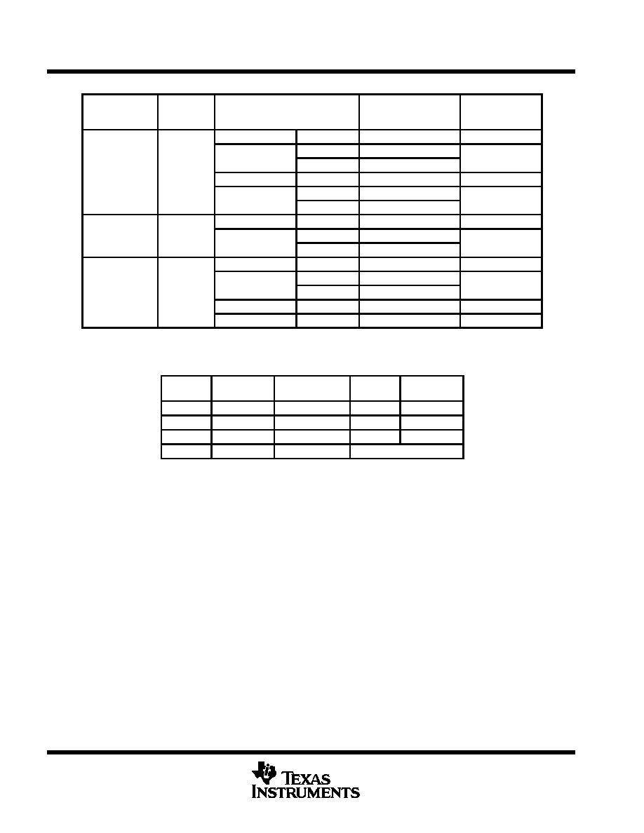
FUNCTION TABLE
RESET
TRIGGER
VOLTAGE
THRESHOLD
VOLTAGE
OUTPUT
DISCHARGE
SWITCH
Low
Irrelevant
Irrelevant
Low
On
High
<1/3 VDD
Irrelevant
High
Off
High
>1/3 VDD
>2/3 VDD
Low
On
High
>1/3 VDD
<2/3 VDD
As previously established
Voltage levels shown are nominal.
NE555, SA555, SE555
PRECISION TIMERS
SLFS022D ≠ SEPTEMBER 1973 ≠ REVISED JUNE 2003
3
POST OFFICE BOX 655303
∑
DALLAS, TEXAS 75265
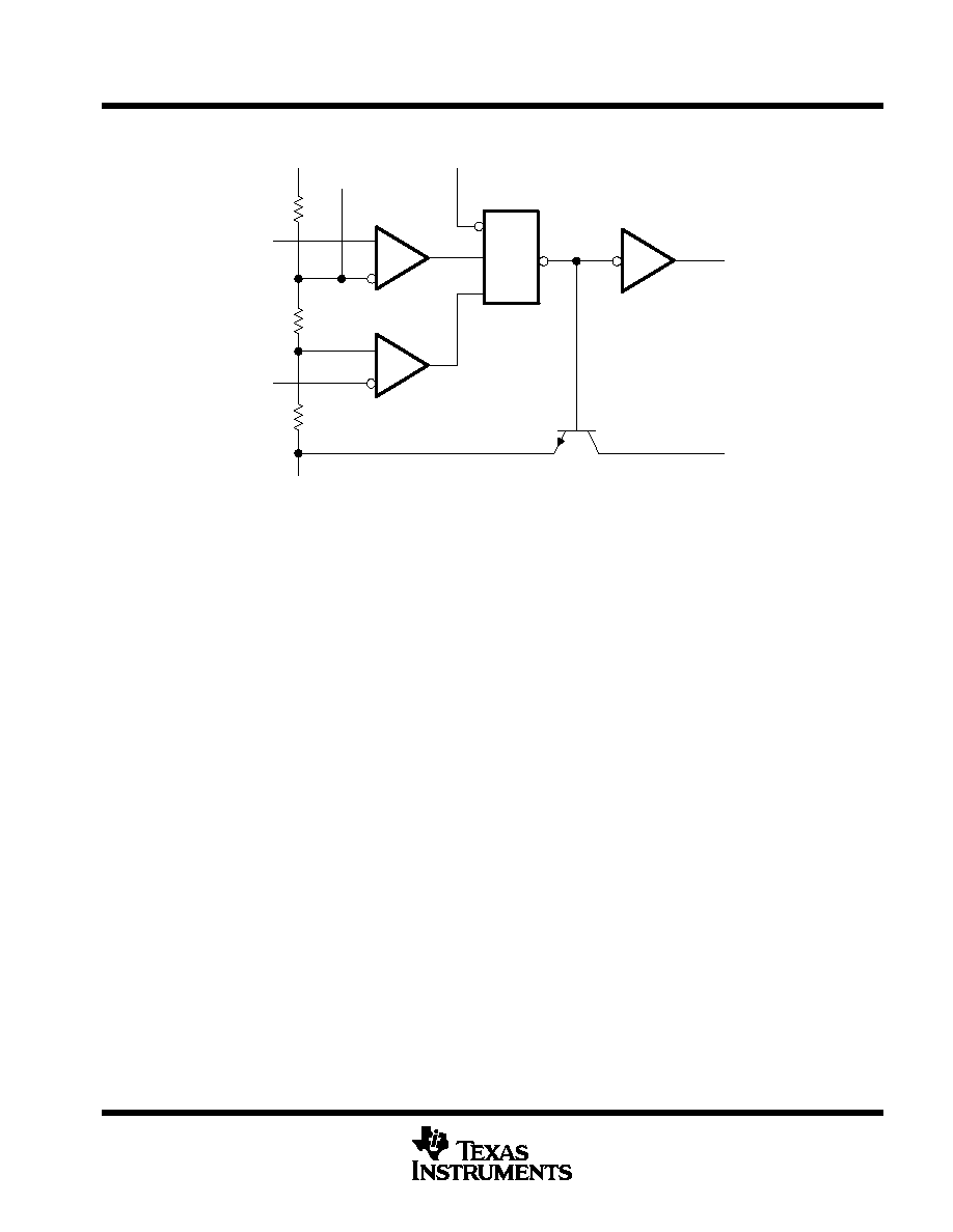
functional block diagram
1
S
R
R1
TRIG
THRES
VCC
CONT
RESET
OUT
DISCH
GND
ŒŒ
Œ
Œ
Œ
Œ
Œ
Œ
Œ
Pin numbers shown are for the D, JG, P, PS, and PW packages.
NOTE A: RESET can override TRIG, which can override THRES.
4
8
5
6
2
1
7
3
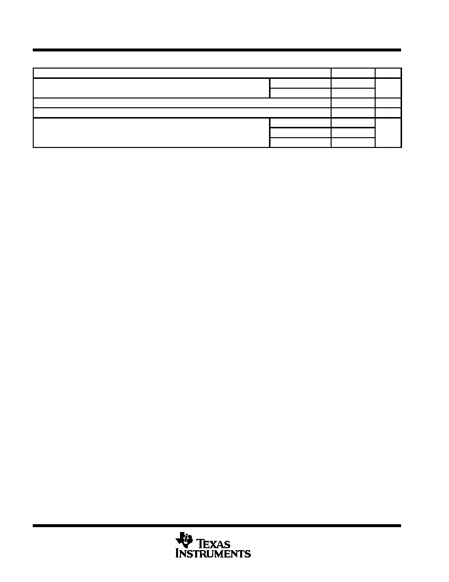
absolute maximum ratings over operating free-air temperature range (unless otherwise noted)
Supply voltage, V
CC
(see Note 1)
18 V
. . . . . . . . . . . . . . . . . . . . . . . . . . . . . . . . . . . . . . . . . . . . . . . . . . . . . . . . . . . .
Input voltage (CONT, RESET, THRES, and TRIG)
V
CC
. . . . . . . . . . . . . . . . . . . . . . . . . . . . . . . . . . . . . . . . . . . . . .
Output current
±
225 mA
. . . . . . . . . . . . . . . . . . . . . . . . . . . . . . . . . . . . . . . . . . . . . . . . . . . . . . . . . . . . . . . . . . . . . . . . .
Package thermal impedance,
JA
(see Notes 2 and 3): D package
97
∞
C/W
. . . . . . . . . . . . . . . . . . . . . . . . . . . .
P package
85
∞
C/W
. . . . . . . . . . . . . . . . . . . . . . . . . . . .
PS package
95
∞
C/W
. . . . . . . . . . . . . . . . . . . . . . . . . . .
PW package
149
∞
C/W
. . . . . . . . . . . . . . . . . . . . . . . . .
Package thermal impedance,
JC
(see Notes 4 and 5): FK package
5.61
∞
C/W
. . . . . . . . . . . . . . . . . . . . . . . . .
JG package
14.5
∞
C/W
. . . . . . . . . . . . . . . . . . . . . . . . .
Operating virtual junction temperature, T
J
150
∞
C
. . . . . . . . . . . . . . . . . . . . . . . . . . . . . . . . . . . . . . . . . . . . . . . . . . .
Case temperature for 60 seconds: FK package
260
∞
C
. . . . . . . . . . . . . . . . . . . . . . . . . . . . . . . . . . . . . . . . . . . . . .
Lead temperature 1,6 mm (1/16 inch) from case for 10 seconds: D, P, PS, or PW package
260
∞
C
. . . . . . . .
Lead temperature 1,6 mm (1/16 inch) from case for 60 seconds: JG package
300
∞
C
. . . . . . . . . . . . . . . . . . . .
Storage temperature range, T
stg
≠65
∞
C to 150
∞
C
. . . . . . . . . . . . . . . . . . . . . . . . . . . . . . . . . . . . . . . . . . . . . . . . . . .
Stresses beyond those listed under "absolute maximum ratings" may cause permanent damage to the device. These are stress ratings only, and
functional operation of the device at these or any other conditions beyond those indicated under "recommended operating conditions" is not
implied. Exposure to absolute-maximum-rated conditions for extended periods may affect device reliability.
NOTES:
1. All voltage values are with respect to GND.
2. Maximum power dissipation is a function of TJ(max),
JA, and TA. The maximum allowable power dissipation at any allowable
ambient temperature is PD = (TJ(max) ≠ TA)/
JA. Operating at the absolute maximum TJ of 150
∞
C can affect reliability.
3. The package thermal impedance is calculated in accordance with JESD 51-7.
4. Maximum power dissipation is a function of TJ(max),
JC, and TC. The maximum allowable power dissipation at any allowable case
temperature is PD = (TJ(max) ≠ TC)/
JC. Operating at the absolute maximum TJ of 150
∞
C can affect reliability.
5. The package thermal impedance is calculated in accordance with MIL-STD-883.
NE555, SA555, SE555
PRECISION TIMERS
SLFS022D ≠ SEPTEMBER 1973 ≠ REVISED JUNE 2003
4
POST OFFICE BOX 655303
∑
DALLAS, TEXAS 75265
recommended operating conditions
MIN
MAX
UNIT
VCC
Supply voltage
SA555, NE555
4.5
16
V
VCC
Supply voltage
SE555
4.5
18
V
VI
Input voltage (CONT, RESET, THRES, and TRIG)
VCC
V
IO
Output current
±
200
mA
NE555
0
70
TA
Operating free-air temperature
SA555
≠40
85
∞
C
SE555
≠55
125
NE555, SA555, SE555
PRECISION TIMERS
SLFS022D ≠ SEPTEMBER 1973 ≠ REVISED JUNE 2003
5
POST OFFICE BOX 655303
∑
DALLAS, TEXAS 75265
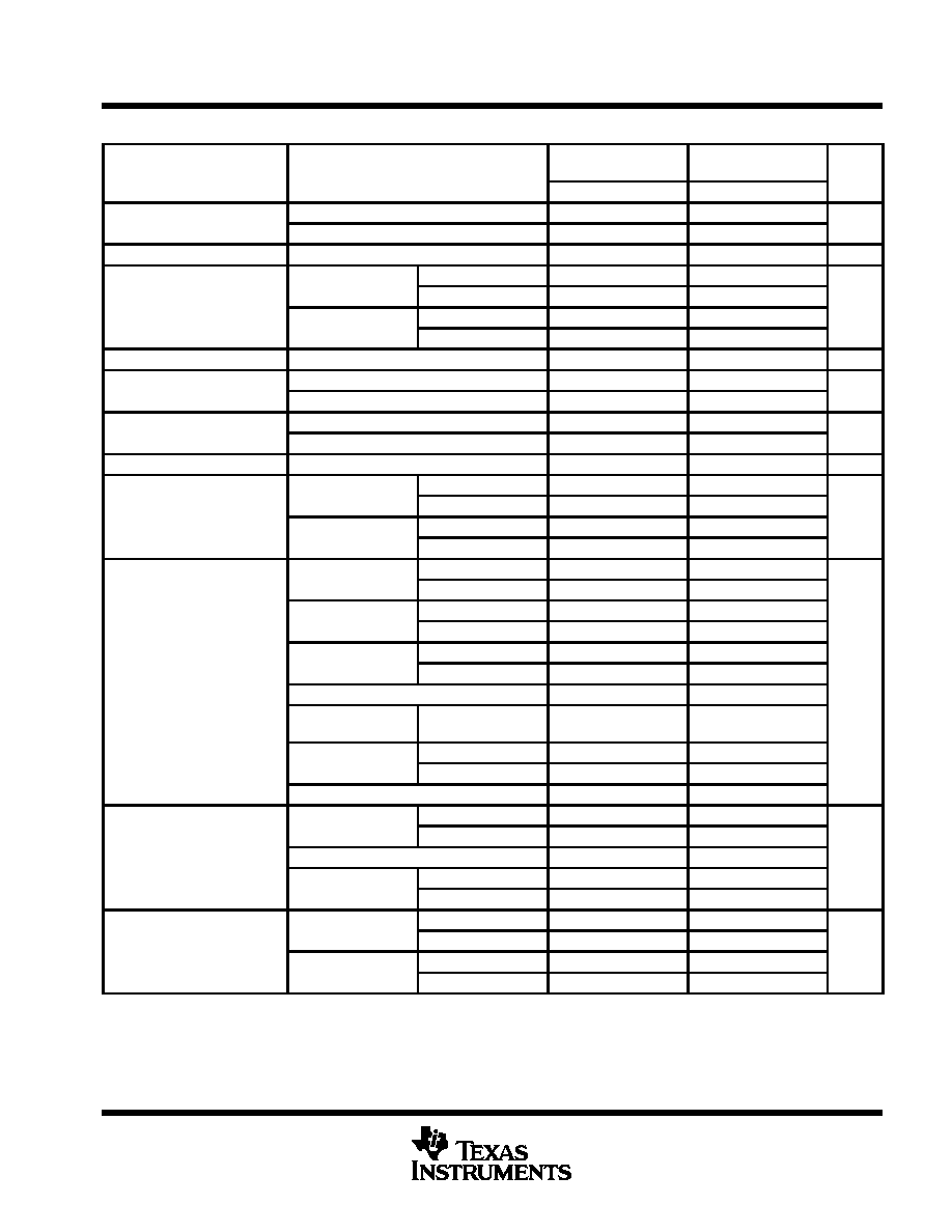
electrical characteristics, V
CC
= 5 V to 15 V, T
A
= 25
∞
C (unless otherwise noted)
PARAMETER
TEST CONDITIONS
SE555
NE555
SA555
UNIT
MIN
TYP
MAX
MIN
TYP
MAX
THRES voltage level
VCC = 15 V
9.4
10
10.6
8.8
10
11.2
V
THRES voltage level
VCC = 5 V
2.7
3.3
4
2.4
3.3
4.2
V
THRES current (see Note 6)
30
250
30
250
nA
VCC = 15 V
4.8
5
5.2
4.5
5
5.6
TRIG voltage level
VCC = 15 V
TA = ≠55
∞
C to 125
∞
C
3
6
V
TRIG voltage level
VCC = 5 V
1.45
1.67
1.9
1.1
1.67
2.2
V
VCC = 5 V
TA = ≠55
∞
C to 125
∞
C
1.9
TRIG current
TRIG at 0 V
0.5
0.9
0.5
2
µ
A
RESET voltage level
0.3
0.7
1
0.3
0.7
1
V
RESET voltage level
TA = ≠55
∞
C to 125
∞
C
1.1
V
RESET current
RESET at VCC
0.1
0.4
0.1
0.4
mA
RESET current
RESET at 0 V
≠0.4
≠1
≠0.4
≠1.5
mA
DISCH switch off-state current
20
100
20
100
nA
VCC = 15 V
9.6
10
10.4
9
10
11
CONT voltage (open circuit)
VCC = 15 V
TA = ≠55
∞
C to 125
∞
C
9.6
10.4
V
CONT voltage (open circuit)
VCC = 5 V
2.9
3.3
3.8
2.6
3.3
4
V
VCC = 5 V
TA = ≠55
∞
C to 125
∞
C
2.9
3.8
VCC = 15 V,
0.1
0.15
0.1
0.25
CC
,
IOL = 10 mA
TA = ≠55
∞
C to 125
∞
C
0.2
VCC = 15 V,
0.4
0.5
0.4
0.75
CC
,
IOL = 50 mA
TA = ≠55
∞
C to 125
∞
C
1
VCC = 15 V,
2
2.2
2
2.5
Low-level output voltage
CC
,
IOL = 100 mA
TA = ≠55
∞
C to 125
∞
C
2.7
V
Low-level out ut voltage
VCC = 15 V,
IOL = 200 mA
2.5
2.5
V
VCC = 5 V,
IOL = 3.5 mA
TA = ≠55
∞
C to 125
∞
C
0.35
VCC = 5 V,
0.1
0.2
0.1
0.35
CC
,
IOL = 5 mA
TA = ≠55
∞
C to 125
∞
C
0.8
VCC = 5 V,
IOL = 8 mA
0.15
0.25
0.15
0.4
VCC = 15 V,
13
13.3
12.75
13.3
CC
,
IOH = ≠100 mA
TA = ≠55
∞
C to 125
∞
C
12
High-level output voltage
VCC = 15 V,
IOH = ≠200 mA
12.5
12.5
V
VCC = 5 V,
3
3.3
2.75
3.3
CC
,
IOH = ≠100 mA
TA = ≠55
∞
C to 125
∞
C
2
Output low,
VCC = 15 V
10
12
10
15
Supply current
,
No load
VCC = 5 V
3
5
3
6
mA
Supply current
Output high,
VCC = 15 V
9
10
9
13
mA
g
No load
VCC = 5 V
2
4
2
5
NOTE 6: This parameter influences the maximum value of the timing resistors RA and RB in the circuit of Figure 12. For example, when
VCC = 5 V, the maximum value is R = RA + RB
3.4 M
, and for VCC = 15 V, the maximum value is 10 M
.