OMAP5910
Dual-Core Processor
Data Manual
Literature Number: SPRS197D
August 2002 - Revised August 2004
Literature Number: SPRS197D
August 2002 - Revised August 2004
PRODUCTION DATA information is current as of publication date.
Products conform to specifications per the terms of Texas Instruments
standard warranty. Production processing does not necessarily include
testing of all parameters.

IMPORTANT NOTICE
Texas Instruments Incorporated and its subsidiaries (TI) reserve the right to make corrections, modifications,
enhancements, improvements, and other changes to its products and services at any time and to discontinue
any product or service without notice. Customers should obtain the latest relevant information before placing
orders and should verify that such information is current and complete. All products are sold subject to TI's terms
and conditions of sale supplied at the time of order acknowledgment.
TI warrants performance of its hardware products to the specifications applicable at the time of sale in
accordance with TI's standard warranty. Testing and other quality control techniques are used to the extent TI
deems necessary to support this warranty. Except where mandated by government requirements, testing of all
parameters of each product is not necessarily performed.
TI assumes no liability for applications assistance or customer product design. Customers are responsible for
their products and applications using TI components. To minimize the risks associated with customer products
and applications, customers should provide adequate design and operating safeguards.
TI does not warrant or represent that any license, either express or implied, is granted under any TI patent right,
copyright, mask work right, or other TI intellectual property right relating to any combination, machine, or process
in which TI products or services are used. Information published by TI regarding third-party products or services
does not constitute a license from TI to use such products or services or a warranty or endorsement thereof.
Use of such information may require a license from a third party under the patents or other intellectual property
of the third party, or a license from TI under the patents or other intellectual property of TI.
Reproduction of information in TI data books or data sheets is permissible only if reproduction is without
alteration and is accompanied by all associated warranties, conditions, limitations, and notices. Reproduction
of this information with alteration is an unfair and deceptive business practice. TI is not responsible or liable for
such altered documentation.
Resale of TI products or services with statements different from or beyond the parameters stated by TI for that
product or service voids all express and any implied warranties for the associated TI product or service and
is an unfair and deceptive business practice. TI is not responsible or liable for any such statements.
Following are URLs where you can obtain information on other Texas Instruments products and application
solutions:
Products
Applications
Amplifiers
amplifier.ti.com
Audio
www.ti.com/audio
Data Converters
dataconverter.ti.com
Automotive
www.ti.com/automotive
DSP
dsp.ti.com
Broadband
www.ti.com/broadband
Interface
interface.ti.com
Digital Control
www.ti.com/digitalcontrol
Logic
logic.ti.com
Military
www.ti.com/military
Power Mgmt
power.ti.com
Optical Networking
www.ti.com/opticalnetwork
Microcontrollers
microcontroller.ti.com
Security
www.ti.com/security
Telephony
www.ti.com/telephony
Video & Imaging
www.ti.com/video
Wireless
www.ti.com/wireless
Mailing Address:
Texas Instruments
Post Office Box 655303 Dallas, Texas 75265
Copyright
2004, Texas Instruments Incorporated

Revision History
3
August 2002 - Revised August 2004
SPRS197D
REVISION HISTORY
This data sheet revision history highlights the technical changes made to the SPRS197C device-specific data
sheet to make it an SPRS197D revision.
Scope: This document has been reviewed for technical accuracy; the technical content is up-to-date as of the
specified release date and includes the following changes.
PAGE(S)
NO.
ADDITIONS/CHANGES/DELETIONS
All
Removed all references to MMC/SD SPI mode that is no longer supported.
18 - 21
In Table 2-1:
Added footnote for GZG pin V12; "See Section 5.6.1 and Section 5.6.2 for special V
SS
considerations with
oscillator circuits."
Changed GZG pin P9 from "USB0.DP" to "USB.DP"
22 - 24
In Table 2-2:
Added footnote for GDY pin F6; "See Section 5.6.1 and Section 5.6.2 for special V
SS
considerations with
oscillator circuits."
Changed GDY pin P5 from "USB0.DP" to "USB.DP"
34 - 46
In Table 2-4:
Added A11, A13, H9, and G9 to list o f V
SS
Pins
Changed U21 to N16 in the GDY column
Changed USB1.TXEN pin in the GDY column from T6 to P14
Changed LCD.PCLK and LCD.P[15:0] description from "LCD panels" to "LCD panel"
Changed SDRAM.CLK description to include "SDRAM.CLK can also be configured as an input to monitor
skew control."
Changed STAT_VAL/WKUP description to remove "STAT_VAL/WKUP may be configured via software to function as an
external wake-up signal to the OMAP5910 device to request chip wake-up during sleep modes."
48
Changed last bullet in Section 3.1
from:
LCD controller supporting monochrome panels or STN and TFT color panels
to:
LCD controller supporting monochrome panels (STN) and color panels (STN or TFT)
54
In Section 3.3.4, changed the last sentence in the first paragraph
from: Accessing registers with the incorrect access width may result in unexpected results including a TI Peripheral
Bus (TIPB) bus error and associated TIPB interrupt.
to:
Accessing registers with the incorrect access width may cause unexpected results including a TI Peripheral Bus
(TIPB) bus error and associated TIPB interrupt.
64
Combined bullets:
�
Selectable UART/autobauding modes (autobauding on UART1 and UART2)
�
Auto bauding between 1200bits/s and 115.2K bits/s
To read as follows:
�
Selectable UART/autobauding modes (autobauding on UART1 and UART2) with autobauding between
1200 bits/s and 115.2K bits/s
66
Revised Section 3.11 to removed bulleted list and replace with the following: "The EMIFF Interface provides access to
16-bit-wide access to standard SDRAM memories and the IMIF provides access to the 192K bytes of on-chip SRAM."
Revision History
4
August 2002 - Revised August 2004
SPRS197D
PAGE(S)
NO.
ADDITIONS/CHANGES/DELETIONS
68
In Section 3.13, removed the following bulleted items:
�
Quantization /Dequantization (useful for JPEG, MPEG, H.26x Encoding/Decoding)
�
Flexible 1D/2D Wavelet Processing (useful for JPEG2000, MPEG4, and other compression standards)
�
Boundary and Perimeter Computation (useful for Machine Vision applications)
�
Image Threshold and Histogram Computations (useful for various Image Analysis applications)
72
Revised Table 3-17 to change access width from 32 bit to 16 bit. Changed MPU_READ_TIM_WD address to FFFE:C804
and changed MPU_TIMER_MODE_WD address to FFFE:C808.
120
Revised Section 4.1 and added Figure 4-1, OMAP Device Nomenclature
126
Changed Section 5.6.2, first paragraph, third line from "If the internal oscillator is not used (configured in software), an ex-
ternal clock source must be applied to the OSC1_IN pin and the OSC1_OUT pin must be left unconnected." to "If the inter-
nal oscillator is not used (configured in software using FUNC_MUX_CTRL_B register), an external clock source must be
applied to the OSC1_IN pin and the OSC1_OUT pin must be left unconnected."
130
Revised Table 5-10
131
Revised Table 5-11
141 - 142
Changed footnote of Table 5-14 from: "P = 1/(Base frequency) for McBSP1 and 3, or 1/(AMPER_CK clock frequency) in
nanoseconds (ns) for McBSP 2.Base frequency is 12 or 13MHz". to: "Regardless of whether MCBSP.CLKS is internally or
externally clocked, P = 1/(DSPXOR_CK) for McBSP1 and McBSP3, and P = 1/(AMPER_CK) for McBSP2. See the
OMAP5910 Dual-Core Processor Clock Generation and System Reset Management Reference Guide (literature number
SPRU678) for additional details."

Contents
5
August 2002 - Revised August 2004
SPRS197D
Contents
Section
Page
1
OMAP5910 Features
15
. . . . . . . . . . . . . . . . . . . . . . . . . . . . . . . . . . . . . . . . . . . . . . . . . . . . . . . . . . . . . . . . . . . .
2
Introduction
16
. . . . . . . . . . . . . . . . . . . . . . . . . . . . . . . . . . . . . . . . . . . . . . . . . . . . . . . . . . . . . . . . . . . . . . . . . . . .
2.1
Description
16
. . . . . . . . . . . . . . . . . . . . . . . . . . . . . . . . . . . . . . . . . . . . . . . . . . . . . . . . . . . . . . . . . . . . . .
2.1.1
TMS320C55x DSP Core
16
. . . . . . . . . . . . . . . . . . . . . . . . . . . . . . . . . . . . . . . . . . . . . . . . .
2.1.2
TI-Enhanced TI925T RISC Processor
17
. . . . . . . . . . . . . . . . . . . . . . . . . . . . . . . . . . . . . .
2.2
Terminal Assignments
18
. . . . . . . . . . . . . . . . . . . . . . . . . . . . . . . . . . . . . . . . . . . . . . . . . . . . . . . . . . . . .
2.3
Terminal Characteristics and Multiplexing
24
. . . . . . . . . . . . . . . . . . . . . . . . . . . . . . . . . . . . . . . . . . . .
2.4
Signal Description
34
. . . . . . . . . . . . . . . . . . . . . . . . . . . . . . . . . . . . . . . . . . . . . . . . . . . . . . . . . . . . . . . .
3
Functional Overview
47
. . . . . . . . . . . . . . . . . . . . . . . . . . . . . . . . . . . . . . . . . . . . . . . . . . . . . . . . . . . . . . . . . . . .
3.1
Functional Block Diagram Features
48
. . . . . . . . . . . . . . . . . . . . . . . . . . . . . . . . . . . . . . . . . . . . . . . . .
3.2
MPU Memory Maps
50
. . . . . . . . . . . . . . . . . . . . . . . . . . . . . . . . . . . . . . . . . . . . . . . . . . . . . . . . . . . . . . .
3.2.1
MPU Global Memory Map
50
. . . . . . . . . . . . . . . . . . . . . . . . . . . . . . . . . . . . . . . . . . . . . . . .
3.2.2
MPU Subsystem Registers Memory Map
51
. . . . . . . . . . . . . . . . . . . . . . . . . . . . . . . . . . .
3.3
DSP Memory Maps
52
. . . . . . . . . . . . . . . . . . . . . . . . . . . . . . . . . . . . . . . . . . . . . . . . . . . . . . . . . . . . . . .
3.3.1
DSP Global Memory Map
52
. . . . . . . . . . . . . . . . . . . . . . . . . . . . . . . . . . . . . . . . . . . . . . . .
3.3.2
On-Chip Dual-Access RAM (DARAM)
53
. . . . . . . . . . . . . . . . . . . . . . . . . . . . . . . . . . . . . .
3.3.3
On-Chip Single-Access RAM (SARAM)
53
. . . . . . . . . . . . . . . . . . . . . . . . . . . . . . . . . . . .
3.3.4
DSP I/O Space Memory Map
54
. . . . . . . . . . . . . . . . . . . . . . . . . . . . . . . . . . . . . . . . . . . . .
3.4
DSP External Memory (Managed by MMU)
55
. . . . . . . . . . . . . . . . . . . . . . . . . . . . . . . . . . . . . . . . . .
3.5
MPU and DSP Private Peripherals
57
. . . . . . . . . . . . . . . . . . . . . . . . . . . . . . . . . . . . . . . . . . . . . . . . . .
3.5.1
Timers
57
. . . . . . . . . . . . . . . . . . . . . . . . . . . . . . . . . . . . . . . . . . . . . . . . . . . . . . . . . . . . . . . . .
3.5.2
32k Timer (MPU only)
57
. . . . . . . . . . . . . . . . . . . . . . . . . . . . . . . . . . . . . . . . . . . . . . . . . . . .
3.5.3
Watchdog Timer
57
. . . . . . . . . . . . . . . . . . . . . . . . . . . . . . . . . . . . . . . . . . . . . . . . . . . . . . . .
3.5.4
Interrupt Handlers
57
. . . . . . . . . . . . . . . . . . . . . . . . . . . . . . . . . . . . . . . . . . . . . . . . . . . . . . .
3.5.5
LCD Controller
57
. . . . . . . . . . . . . . . . . . . . . . . . . . . . . . . . . . . . . . . . . . . . . . . . . . . . . . . . . .
3.6
MPU Public Peripherals
58
. . . . . . . . . . . . . . . . . . . . . . . . . . . . . . . . . . . . . . . . . . . . . . . . . . . . . . . . . . .
3.6.1
USB Host Controller
58
. . . . . . . . . . . . . . . . . . . . . . . . . . . . . . . . . . . . . . . . . . . . . . . . . . . . .
3.6.2
USB Function Peripheral
59
. . . . . . . . . . . . . . . . . . . . . . . . . . . . . . . . . . . . . . . . . . . . . . . . .
3.6.3
Multichannel Buffered Serial Port (McBSP)
59
. . . . . . . . . . . . . . . . . . . . . . . . . . . . . . . . .
3.6.4
I
2
C Master/Slave Interface
60
. . . . . . . . . . . . . . . . . . . . . . . . . . . . . . . . . . . . . . . . . . . . . . .
3.6.5
MICROWIRE Serial Interface
60
. . . . . . . . . . . . . . . . . . . . . . . . . . . . . . . . . . . . . . . . . . . . .
3.6.6
Multimedia Card/Secure Digital (MMC/SD) Interface
60
. . . . . . . . . . . . . . . . . . . . . . . . .
3.6.7
HDQ/1-Wire Interface
61
. . . . . . . . . . . . . . . . . . . . . . . . . . . . . . . . . . . . . . . . . . . . . . . . . . . .
3.6.8
Camera Interface
61
. . . . . . . . . . . . . . . . . . . . . . . . . . . . . . . . . . . . . . . . . . . . . . . . . . . . . . .
3.6.9
MPUIO/Keyboard Interface
61
. . . . . . . . . . . . . . . . . . . . . . . . . . . . . . . . . . . . . . . . . . . . . . .
3.6.10
Pulse-Width Light (PWL)
61
. . . . . . . . . . . . . . . . . . . . . . . . . . . . . . . . . . . . . . . . . . . . . . . . .
3.6.11
Pulse-Width Tone (PWT)
61
. . . . . . . . . . . . . . . . . . . . . . . . . . . . . . . . . . . . . . . . . . . . . . . . .
3.6.12
LED Pulse Generator
62
. . . . . . . . . . . . . . . . . . . . . . . . . . . . . . . . . . . . . . . . . . . . . . . . . . . .
3.6.13
Real-Time Clock
62
. . . . . . . . . . . . . . . . . . . . . . . . . . . . . . . . . . . . . . . . . . . . . . . . . . . . . . . .
3.6.14
Frame Adjustment Counter
62
. . . . . . . . . . . . . . . . . . . . . . . . . . . . . . . . . . . . . . . . . . . . . . .
3.7
DSP Public Peripherals
62
. . . . . . . . . . . . . . . . . . . . . . . . . . . . . . . . . . . . . . . . . . . . . . . . . . . . . . . . . . . .
3.7.1
Multichannel Buffered Serial Port (McBSP)
62
. . . . . . . . . . . . . . . . . . . . . . . . . . . . . . . . .
3.7.2
Multichannel Serial Interface (MCSI)
63
. . . . . . . . . . . . . . . . . . . . . . . . . . . . . . . . . . . . . . .

Contents
6
August 2002 - Revised August 2004
SPRS197D
Section
Page
3.8
Shared Peripherals
63
. . . . . . . . . . . . . . . . . . . . . . . . . . . . . . . . . . . . . . . . . . . . . . . . . . . . . . . . . . . . . . .
3.8.1
Universal Asynchronous Receiver/Transmitter (UART)
63
. . . . . . . . . . . . . . . . . . . . . . .
3.8.2
General-Purpose I/O (GPIO)
64
. . . . . . . . . . . . . . . . . . . . . . . . . . . . . . . . . . . . . . . . . . . . . .
3.8.3
Mailbox Registers
64
. . . . . . . . . . . . . . . . . . . . . . . . . . . . . . . . . . . . . . . . . . . . . . . . . . . . . . .
3.9
System DMA Controller
65
. . . . . . . . . . . . . . . . . . . . . . . . . . . . . . . . . . . . . . . . . . . . . . . . . . . . . . . . . . . .
3.10
DSP DMA Controller
66
. . . . . . . . . . . . . . . . . . . . . . . . . . . . . . . . . . . . . . . . . . . . . . . . . . . . . . . . . . . . . .
3.11
Traffic Controller (Memory Interfaces)
66
. . . . . . . . . . . . . . . . . . . . . . . . . . . . . . . . . . . . . . . . . . . . . . .
3.12
Interprocessor Communication
67
. . . . . . . . . . . . . . . . . . . . . . . . . . . . . . . . . . . . . . . . . . . . . . . . . . . . .
3.12.1
MPU/DSP Mailbox Registers
67
. . . . . . . . . . . . . . . . . . . . . . . . . . . . . . . . . . . . . . . . . . . . .
3.12.2
MPU Interface (MPUI)
67
. . . . . . . . . . . . . . . . . . . . . . . . . . . . . . . . . . . . . . . . . . . . . . . . . . .
3.12.3
MPU/DSP Shared Memory
68
. . . . . . . . . . . . . . . . . . . . . . . . . . . . . . . . . . . . . . . . . . . . . . .
3.13
DSP Hardware Accelerators
68
. . . . . . . . . . . . . . . . . . . . . . . . . . . . . . . . . . . . . . . . . . . . . . . . . . . . . . .
3.13.1
DCT/iDCT Accelerator
68
. . . . . . . . . . . . . . . . . . . . . . . . . . . . . . . . . . . . . . . . . . . . . . . . . . .
3.13.2
Motion Estimation Accelerator
68
. . . . . . . . . . . . . . . . . . . . . . . . . . . . . . . . . . . . . . . . . . . .
3.13.3
Pixel Interpolation Accelerator
68
. . . . . . . . . . . . . . . . . . . . . . . . . . . . . . . . . . . . . . . . . . . .
3.14
Power Supply Connection Examples
68
. . . . . . . . . . . . . . . . . . . . . . . . . . . . . . . . . . . . . . . . . . . . . . . .
3.14.1
Core and I/O Voltage Supply Connections
68
. . . . . . . . . . . . . . . . . . . . . . . . . . . . . . . . . .
3.14.2
Core Voltage Noise Isolation
70
. . . . . . . . . . . . . . . . . . . . . . . . . . . . . . . . . . . . . . . . . . . . . .
3.15
MPU Register Descriptions
71
. . . . . . . . . . . . . . . . . . . . . . . . . . . . . . . . . . . . . . . . . . . . . . . . . . . . . . . .
3.15.1
MPU Private Peripheral Registers
72
. . . . . . . . . . . . . . . . . . . . . . . . . . . . . . . . . . . . . . . . .
3.15.2
MPU Public Peripheral Registers
79
. . . . . . . . . . . . . . . . . . . . . . . . . . . . . . . . . . . . . . . . . .
3.15.3
MPU Configuration Registers
88
. . . . . . . . . . . . . . . . . . . . . . . . . . . . . . . . . . . . . . . . . . . . .
3.16
DSP Register Descriptions
95
. . . . . . . . . . . . . . . . . . . . . . . . . . . . . . . . . . . . . . . . . . . . . . . . . . . . . . . . .
3.16.1
DSP Private Peripheral Registers
95
. . . . . . . . . . . . . . . . . . . . . . . . . . . . . . . . . . . . . . . . .
3.16.2
DSP Public Peripheral Registers
101
. . . . . . . . . . . . . . . . . . . . . . . . . . . . . . . . . . . . . . . . . .
3.16.3
DSP Configuration Registers
106
. . . . . . . . . . . . . . . . . . . . . . . . . . . . . . . . . . . . . . . . . . . . .
3.16.4
MPU/DSP Shared Peripheral Register Descriptions
108
. . . . . . . . . . . . . . . . . . . . . . . . . .
3.17
Interrupts
113
. . . . . . . . . . . . . . . . . . . . . . . . . . . . . . . . . . . . . . . . . . . . . . . . . . . . . . . . . . . . . . . . . . . . . . . .
3.18
MPU System DMA Request Mapping
117
. . . . . . . . . . . . . . . . . . . . . . . . . . . . . . . . . . . . . . . . . . . . . . . .
3.19
DSP DMA Event Mapping
118
. . . . . . . . . . . . . . . . . . . . . . . . . . . . . . . . . . . . . . . . . . . . . . . . . . . . . . . . .
4
Documentation Support
119
. . . . . . . . . . . . . . . . . . . . . . . . . . . . . . . . . . . . . . . . . . . . . . . . . . . . . . . . . . . . . . . . .
4.1
Device and Development Tool Support Nomenclature
120
. . . . . . . . . . . . . . . . . . . . . . . . . . . . . . . . . .
5
Electrical Specifications
121
. . . . . . . . . . . . . . . . . . . . . . . . . . . . . . . . . . . . . . . . . . . . . . . . . . . . . . . . . . . . . . . .
5.1
Absolute Maximum Ratings
121
. . . . . . . . . . . . . . . . . . . . . . . . . . . . . . . . . . . . . . . . . . . . . . . . . . . . . . . .
5.2
Recommended Operating Conditions
122
. . . . . . . . . . . . . . . . . . . . . . . . . . . . . . . . . . . . . . . . . . . . . . . .
5.3
Electrical Characteristics Over Recommended Operating Case Temperature
Range (Unless Otherwise Noted)
123
. . . . . . . . . . . . . . . . . . . . . . . . . . . . . . . . . . . . . . . . . . . . . . . . . . .
5.4
Package Thermal Resistance Characteristics
124
. . . . . . . . . . . . . . . . . . . . . . . . . . . . . . . . . . . . . . . . .
5.5
Timing Parameter Symbology
124
. . . . . . . . . . . . . . . . . . . . . . . . . . . . . . . . . . . . . . . . . . . . . . . . . . . . . .
5.6
Clock Specifications
125
. . . . . . . . . . . . . . . . . . . . . . . . . . . . . . . . . . . . . . . . . . . . . . . . . . . . . . . . . . . . . . .
5.6.1
32-kHz Oscillator and Input Clock
125
. . . . . . . . . . . . . . . . . . . . . . . . . . . . . . . . . . . . . . . . .
5.6.2
Base Oscillator (12 MHz or 13 MHz) and Input Clock
126
. . . . . . . . . . . . . . . . . . . . . . . . .
5.6.3
Internal Clock Speed Limitations
127
. . . . . . . . . . . . . . . . . . . . . . . . . . . . . . . . . . . . . . . . . .
5.7
Reset Timings
128
. . . . . . . . . . . . . . . . . . . . . . . . . . . . . . . . . . . . . . . . . . . . . . . . . . . . . . . . . . . . . . . . . . . .
5.7.1
OMAP5910 Device Reset
128
. . . . . . . . . . . . . . . . . . . . . . . . . . . . . . . . . . . . . . . . . . . . . . . .
5.7.2
OMAP5910 MPU Core Reset
129
. . . . . . . . . . . . . . . . . . . . . . . . . . . . . . . . . . . . . . . . . . . . .

Contents
7
August 2002 - Revised August 2004
SPRS197D
Section
Page
5.8
External Memory Interface Timing
130
. . . . . . . . . . . . . . . . . . . . . . . . . . . . . . . . . . . . . . . . . . . . . . . . . . .
5.8.1
EMIFS/Flash Interface Timing
130
. . . . . . . . . . . . . . . . . . . . . . . . . . . . . . . . . . . . . . . . . . . . .
5.8.2
EMIFF/SDRAM Interface Timing
137
. . . . . . . . . . . . . . . . . . . . . . . . . . . . . . . . . . . . . . . . . .
5.9
Multichannel Buffered Serial Port (McBSP) Timings
141
. . . . . . . . . . . . . . . . . . . . . . . . . . . . . . . . . . .
5.9.1
McBSP Transmit and Receive Timings
141
. . . . . . . . . . . . . . . . . . . . . . . . . . . . . . . . . . . . .
5.9.2
McBSP as SPI Master or Slave Timing
145
. . . . . . . . . . . . . . . . . . . . . . . . . . . . . . . . . . . . .
5.10
Multichannel Serial Interface (MCSI)
149
. . . . . . . . . . . . . . . . . . . . . . . . . . . . . . . . . . . . . . . . . . . . . . . .
5.11
Camera Interface Timings
151
. . . . . . . . . . . . . . . . . . . . . . . . . . . . . . . . . . . . . . . . . . . . . . . . . . . . . . . . . .
5.12
LCD Controller Timings
152
. . . . . . . . . . . . . . . . . . . . . . . . . . . . . . . . . . . . . . . . . . . . . . . . . . . . . . . . . . . .
5.13
Multimedia Card/Secure Digital (MMC/SD) Timings
154
. . . . . . . . . . . . . . . . . . . . . . . . . . . . . . . . . . . .
5.14
I
2
C Timings
156
. . . . . . . . . . . . . . . . . . . . . . . . . . . . . . . . . . . . . . . . . . . . . . . . . . . . . . . . . . . . . . . . . . . . . .
5.15
Universal Serial Bus (USB) Timings
157
. . . . . . . . . . . . . . . . . . . . . . . . . . . . . . . . . . . . . . . . . . . . . . . . .
5.16
MICROWIRE Interface Timings
158
. . . . . . . . . . . . . . . . . . . . . . . . . . . . . . . . . . . . . . . . . . . . . . . . . . . . .
5.17
HDQ/1-Wire Interface Timings
159
. . . . . . . . . . . . . . . . . . . . . . . . . . . . . . . . . . . . . . . . . . . . . . . . . . . . . .
6
Glossary
161
. . . . . . . . . . . . . . . . . . . . . . . . . . . . . . . . . . . . . . . . . . . . . . . . . . . . . . . . . . . . . . . . . . . . . . . . . . . . . . .
7
Mechanical Data
164
. . . . . . . . . . . . . . . . . . . . . . . . . . . . . . . . . . . . . . . . . . . . . . . . . . . . . . . . . . . . . . . . . . . . . . . .

Contents
8
August 2002 - Revised August 2004
SPRS197D

Figures
9
August 2002 - Revised August 2004
SPRS197D
List of Figures
Figure
Page
2-1
OMAP5910 GZG MicroStar BGA Package (Bottom View)
18
. . . . . . . . . . . . . . . . . . . . . . . . . . . . . . . . .
2-2
OMAP5910 GDY Package (Bottom View)
21
. . . . . . . . . . . . . . . . . . . . . . . . . . . . . . . . . . . . . . . . . . . . . . .
3-1
OMAP5910 Functional Block Diagram
47
. . . . . . . . . . . . . . . . . . . . . . . . . . . . . . . . . . . . . . . . . . . . . . . . . .
3-2
DSP MMU Off
55
. . . . . . . . . . . . . . . . . . . . . . . . . . . . . . . . . . . . . . . . . . . . . . . . . . . . . . . . . . . . . . . . . . . . . . .
3-3
DSP MMU On
56
. . . . . . . . . . . . . . . . . . . . . . . . . . . . . . . . . . . . . . . . . . . . . . . . . . . . . . . . . . . . . . . . . . . . . . .
3-4
Supply Connections for a Typical System
69
. . . . . . . . . . . . . . . . . . . . . . . . . . . . . . . . . . . . . . . . . . . . . . . .
3-5
Supply Connections for a System With 1.8-V SDRAM
70
. . . . . . . . . . . . . . . . . . . . . . . . . . . . . . . . . . . . .
3-6
External RC Circuit for DPLL CVDD Noise Isolation
71
. . . . . . . . . . . . . . . . . . . . . . . . . . . . . . . . . . . . . . .
5-1
Tester Pin Electronics
124
. . . . . . . . . . . . . . . . . . . . . . . . . . . . . . . . . . . . . . . . . . . . . . . . . . . . . . . . . . . . . . . . .
5-2
32-kHz Oscillator External Crystal
125
. . . . . . . . . . . . . . . . . . . . . . . . . . . . . . . . . . . . . . . . . . . . . . . . . . . . . .
5-3
32-kHz Input Clock
126
. . . . . . . . . . . . . . . . . . . . . . . . . . . . . . . . . . . . . . . . . . . . . . . . . . . . . . . . . . . . . . . . . . .
5-4
Internal System Oscillator External Crystal
126
. . . . . . . . . . . . . . . . . . . . . . . . . . . . . . . . . . . . . . . . . . . . . . .
5-5
Device Reset Timings
128
. . . . . . . . . . . . . . . . . . . . . . . . . . . . . . . . . . . . . . . . . . . . . . . . . . . . . . . . . . . . . . . . .
5-6
MPU Core Reset Timings
129
. . . . . . . . . . . . . . . . . . . . . . . . . . . . . . . . . . . . . . . . . . . . . . . . . . . . . . . . . . . . .
5-7
Asynchronous Memory Read Timing
132
. . . . . . . . . . . . . . . . . . . . . . . . . . . . . . . . . . . . . . . . . . . . . . . . . . . .
5-8
Asynchronous 32-Bit Read
133
. . . . . . . . . . . . . . . . . . . . . . . . . . . . . . . . . . . . . . . . . . . . . . . . . . . . . . . . . . . .
5-9
Asynchronous Read - Page Mode ROM
134
. . . . . . . . . . . . . . . . . . . . . . . . . . . . . . . . . . . . . . . . . . . . . . . .
5-10
Asynchronous Memory Write Timing
135
. . . . . . . . . . . . . . . . . . . . . . . . . . . . . . . . . . . . . . . . . . . . . . . . . . . .
5-11
Synchronous Burst Read
136
. . . . . . . . . . . . . . . . . . . . . . . . . . . . . . . . . . . . . . . . . . . . . . . . . . . . . . . . . . . . . .
5-12
32-Bit (2 x 16-Bit) SDRAM RD (Read) Command (Active Row)
138
. . . . . . . . . . . . . . . . . . . . . . . . . . . . .
5-13
32-Bit (2 x 16-Bit) SDRAM WRT (Write) Command (Active Row)
138
. . . . . . . . . . . . . . . . . . . . . . . . . . .
5-14
SDRAM ACTV (Activate Row) Command
139
. . . . . . . . . . . . . . . . . . . . . . . . . . . . . . . . . . . . . . . . . . . . . . . .
5-15
SDRAM DCAB (Precharge/Deactivate Row) Command
139
. . . . . . . . . . . . . . . . . . . . . . . . . . . . . . . . . . .
5-16
SDRAM REFR (Refresh) Command
140
. . . . . . . . . . . . . . . . . . . . . . . . . . . . . . . . . . . . . . . . . . . . . . . . . . . .
5-17
SDRAM MRS (Mode Register Set) Command
140
. . . . . . . . . . . . . . . . . . . . . . . . . . . . . . . . . . . . . . . . . . . .
5-18
McBSP Receive Timings
144
. . . . . . . . . . . . . . . . . . . . . . . . . . . . . . . . . . . . . . . . . . . . . . . . . . . . . . . . . . . . . .
5-19
McBSP Transmit Timings
144
. . . . . . . . . . . . . . . . . . . . . . . . . . . . . . . . . . . . . . . . . . . . . . . . . . . . . . . . . . . . . .
5-20
McBSP Timing as SPI Master or Slave: CLKSTP = 10b, CLKXP = 0
145
. . . . . . . . . . . . . . . . . . . . . . . .
5-21
McBSP Timing as SPI Master or Slave: CLKSTP = 11b, CLKXP = 0
146
. . . . . . . . . . . . . . . . . . . . . . . .
5-22
McBSP Timing as SPI Master or Slave: CLKSTP = 10b, CLKXP = 1
147
. . . . . . . . . . . . . . . . . . . . . . . .
5-23
McBSP Timing as SPI Master or Slave: CLKSTP = 11b, CLKXP = 1
148
. . . . . . . . . . . . . . . . . . . . . . . .
5-24
MCSI Master Mode Timings
150
. . . . . . . . . . . . . . . . . . . . . . . . . . . . . . . . . . . . . . . . . . . . . . . . . . . . . . . . . . .
5-25
MCSI Slave Mode Timings
150
. . . . . . . . . . . . . . . . . . . . . . . . . . . . . . . . . . . . . . . . . . . . . . . . . . . . . . . . . . . .
5-26
Camera Interface Timings
151
. . . . . . . . . . . . . . . . . . . . . . . . . . . . . . . . . . . . . . . . . . . . . . . . . . . . . . . . . . . . .
5-27
TFT Mode (LCD.HS/LCD.VS on Falling and LCD.Px on Rising LCD.PCLK)
152
. . . . . . . . . . . . . . . . . .
5-28
TFT Mode (LCD.HS/LCD.VS on Rising and LCD.Px on Falling LCD.PCLK)
153
. . . . . . . . . . . . . . . . . .
5-29
MMC/SD Host Command Timings
154
. . . . . . . . . . . . . . . . . . . . . . . . . . . . . . . . . . . . . . . . . . . . . . . . . . . . . .

Figures
10
August 2002 - Revised August 2004
SPRS197D
5-30
MMC/SD Card Response Timings
154
. . . . . . . . . . . . . . . . . . . . . . . . . . . . . . . . . . . . . . . . . . . . . . . . . . . . . .
5-31
MMC/SD Host Write Timings
155
. . . . . . . . . . . . . . . . . . . . . . . . . . . . . . . . . . . . . . . . . . . . . . . . . . . . . . . . . . .
5-32
MMC/SD Host Read and Card CRC Status Timings
155
. . . . . . . . . . . . . . . . . . . . . . . . . . . . . . . . . . . . . . .
5-33
I
2
C Timings
156
. . . . . . . . . . . . . . . . . . . . . . . . . . . . . . . . . . . . . . . . . . . . . . . . . . . . . . . . . . . . . . . . . . . . . . . . . .
5-34
USB Integrated Transceiver Interface Timings
157
. . . . . . . . . . . . . . . . . . . . . . . . . . . . . . . . . . . . . . . . . . . .
5-35
MICROWIRE Timings
158
. . . . . . . . . . . . . . . . . . . . . . . . . . . . . . . . . . . . . . . . . . . . . . . . . . . . . . . . . . . . . . . . .
5-36
OMAP5910 HDQ Interface Reading From HDQ Slave Device
160
. . . . . . . . . . . . . . . . . . . . . . . . . . . . . .
5-37
OMAP5910 HDQ Interface Writing to HDQ Slave Device
160
. . . . . . . . . . . . . . . . . . . . . . . . . . . . . . . . . .
5-38
Typical Communication Between OMAP5910 HDQ and HDQ Slave
160
. . . . . . . . . . . . . . . . . . . . . . . . .
5-39
HDQ/1-Wire Break (Reset) Timing
160
. . . . . . . . . . . . . . . . . . . . . . . . . . . . . . . . . . . . . . . . . . . . . . . . . . . . . .

Tables
11
August 2002 - Revised August 2004
SPRS197D
List of Tables
Table
Page
2-1
GZG BGA Terminal Assignments
18
. . . . . . . . . . . . . . . . . . . . . . . . . . . . . . . . . . . . . . . . . . . . . . . . . . . . .
2-2
GDY BGA Terminal Assignments
22
. . . . . . . . . . . . . . . . . . . . . . . . . . . . . . . . . . . . . . . . . . . . . . . . . . . . .
2-3
Terminal Characteristics and Multiplexing
25
. . . . . . . . . . . . . . . . . . . . . . . . . . . . . . . . . . . . . . . . . . . . . .
2-4
Signal Description
34
. . . . . . . . . . . . . . . . . . . . . . . . . . . . . . . . . . . . . . . . . . . . . . . . . . . . . . . . . . . . . . . . . .
3-1
OMAP5910 MPU Global Memory Map
50
. . . . . . . . . . . . . . . . . . . . . . . . . . . . . . . . . . . . . . . . . . . . . . . . . .
3-2
MPU Private Peripheral Registers
51
. . . . . . . . . . . . . . . . . . . . . . . . . . . . . . . . . . . . . . . . . . . . . . . . . . . . . .
3-3
MPU Public Peripheral Registers
51
. . . . . . . . . . . . . . . . . . . . . . . . . . . . . . . . . . . . . . . . . . . . . . . . . . . . . .
3-4
MPU/DSP Shared Peripheral Registers
51
. . . . . . . . . . . . . . . . . . . . . . . . . . . . . . . . . . . . . . . . . . . . . . . . .
3-5
DSP Public Peripheral Registers (Accessible via MPUI Port)
52
. . . . . . . . . . . . . . . . . . . . . . . . . . . . . .
3-6
MPU Configuration Registers
52
. . . . . . . . . . . . . . . . . . . . . . . . . . . . . . . . . . . . . . . . . . . . . . . . . . . . . . . . . .
3-7
DSP Global Memory Map
52
. . . . . . . . . . . . . . . . . . . . . . . . . . . . . . . . . . . . . . . . . . . . . . . . . . . . . . . . . . . . .
3-8
DARAM Blocks
53
. . . . . . . . . . . . . . . . . . . . . . . . . . . . . . . . . . . . . . . . . . . . . . . . . . . . . . . . . . . . . . . . . . . . . .
3-9
SARAM Blocks
53
. . . . . . . . . . . . . . . . . . . . . . . . . . . . . . . . . . . . . . . . . . . . . . . . . . . . . . . . . . . . . . . . . . . . . .
3-10
DSP Private Peripheral Registers
54
. . . . . . . . . . . . . . . . . . . . . . . . . . . . . . . . . . . . . . . . . . . . . . . . . . . . . .
3-11
DSP Public Peripheral Registers
54
. . . . . . . . . . . . . . . . . . . . . . . . . . . . . . . . . . . . . . . . . . . . . . . . . . . . . . .
3-12
DSP/MPU Shared Peripheral Registers
54
. . . . . . . . . . . . . . . . . . . . . . . . . . . . . . . . . . . . . . . . . . . . . . . . .
3-13
DSP Configuration Registers
54
. . . . . . . . . . . . . . . . . . . . . . . . . . . . . . . . . . . . . . . . . . . . . . . . . . . . . . . . . .
3-14
MPU Timer 1 Registers
72
. . . . . . . . . . . . . . . . . . . . . . . . . . . . . . . . . . . . . . . . . . . . . . . . . . . . . . . . . . . . . . .
3-15
MPU Timer 2 Registers
72
. . . . . . . . . . . . . . . . . . . . . . . . . . . . . . . . . . . . . . . . . . . . . . . . . . . . . . . . . . . . . . .
3-16
MPU Timer 3 Registers
72
. . . . . . . . . . . . . . . . . . . . . . . . . . . . . . . . . . . . . . . . . . . . . . . . . . . . . . . . . . . . . . .
3-17
MPU Watchdog Timer Registers
72
. . . . . . . . . . . . . . . . . . . . . . . . . . . . . . . . . . . . . . . . . . . . . . . . . . . . . . .
3-18
MPU Level 1 Interrupt Handler Registers
73
. . . . . . . . . . . . . . . . . . . . . . . . . . . . . . . . . . . . . . . . . . . . . . .
3-19
MPU Level 2 Interrupt Handler Registers
74
. . . . . . . . . . . . . . . . . . . . . . . . . . . . . . . . . . . . . . . . . . . . . . .
3-20
System DMA Controller Registers
75
. . . . . . . . . . . . . . . . . . . . . . . . . . . . . . . . . . . . . . . . . . . . . . . . . . . .
3-21
LCD Controller Registers
78
. . . . . . . . . . . . . . . . . . . . . . . . . . . . . . . . . . . . . . . . . . . . . . . . . . . . . . . . . . . . .
3-22
McBSP2 Registers
80
. . . . . . . . . . . . . . . . . . . . . . . . . . . . . . . . . . . . . . . . . . . . . . . . . . . . . . . . . . . . . . . . . . .
3-23
MICROWIRE Registers
80
. . . . . . . . . . . . . . . . . . . . . . . . . . . . . . . . . . . . . . . . . . . . . . . . . . . . . . . . . . . . . .
3-24
I
2
C Registers
81
. . . . . . . . . . . . . . . . . . . . . . . . . . . . . . . . . . . . . . . . . . . . . . . . . . . . . . . . . . . . . . . . . . . . . . .
3-25
HDQ/1-Wire Interface Registers
81
. . . . . . . . . . . . . . . . . . . . . . . . . . . . . . . . . . . . . . . . . . . . . . . . . . . . . . .
3-26
MMC/SD Registers
82
. . . . . . . . . . . . . . . . . . . . . . . . . . . . . . . . . . . . . . . . . . . . . . . . . . . . . . . . . . . . . . . . . .
3-27
USB Function Registers
83
. . . . . . . . . . . . . . . . . . . . . . . . . . . . . . . . . . . . . . . . . . . . . . . . . . . . . . . . . . . . .
3-28
USB Host Controller Registers
85
. . . . . . . . . . . . . . . . . . . . . . . . . . . . . . . . . . . . . . . . . . . . . . . . . . . . . . . .
3-29
Camera Interface Registers
85
. . . . . . . . . . . . . . . . . . . . . . . . . . . . . . . . . . . . . . . . . . . . . . . . . . . . . . . . . . .
3-30
MPU I/O/Keyboard Registers
86
. . . . . . . . . . . . . . . . . . . . . . . . . . . . . . . . . . . . . . . . . . . . . . . . . . . . . . . . . .
3-31
PWL Registers
86
. . . . . . . . . . . . . . . . . . . . . . . . . . . . . . . . . . . . . . . . . . . . . . . . . . . . . . . . . . . . . . . . . . . . . .
3-32
PWT Registers
86
. . . . . . . . . . . . . . . . . . . . . . . . . . . . . . . . . . . . . . . . . . . . . . . . . . . . . . . . . . . . . . . . . . . . . .
3-33
LED Pulse Generator 1 Registers
86
. . . . . . . . . . . . . . . . . . . . . . . . . . . . . . . . . . . . . . . . . . . . . . . . . . . . . .
3-34
LED Pulse Generator 2 Registers
86
. . . . . . . . . . . . . . . . . . . . . . . . . . . . . . . . . . . . . . . . . . . . . . . . . . . . . .
3-35
32k Timer Registers
86
. . . . . . . . . . . . . . . . . . . . . . . . . . . . . . . . . . . . . . . . . . . . . . . . . . . . . . . . . . . . . . . . . .
3-36
Real-Time Clock Registers
87
. . . . . . . . . . . . . . . . . . . . . . . . . . . . . . . . . . . . . . . . . . . . . . . . . . . . . . . . . . . .
3-37
Frame Adjustment Counter Registers
87
. . . . . . . . . . . . . . . . . . . . . . . . . . . . . . . . . . . . . . . . . . . . . . . . . .
3-38
OMAP 5910 Pin Configuration Registers
89
. . . . . . . . . . . . . . . . . . . . . . . . . . . . . . . . . . . . . . . . . . . . . . . .
3-39
Local Bus Control Registers
89
. . . . . . . . . . . . . . . . . . . . . . . . . . . . . . . . . . . . . . . . . . . . . . . . . . . . . . . . . . .
3-40
Local Bus MMU Registers
90
. . . . . . . . . . . . . . . . . . . . . . . . . . . . . . . . . . . . . . . . . . . . . . . . . . . . . . . . . . . .
3-41
DSP MMU Registers
91
. . . . . . . . . . . . . . . . . . . . . . . . . . . . . . . . . . . . . . . . . . . . . . . . . . . . . . . . . . . . . . . . .

Tables
12
August 2002 - Revised August 2004
SPRS197D
Table
Page
3-42
MPUI Registers
91
. . . . . . . . . . . . . . . . . . . . . . . . . . . . . . . . . . . . . . . . . . . . . . . . . . . . . . . . . . . . . . . . . . . . .
3-43
TIPB (Private) Bridge 1 Configuration Registers
91
. . . . . . . . . . . . . . . . . . . . . . . . . . . . . . . . . . . . . . . . .
3-44
TIPB (Public) Bridge 2 Configuration Registers
92
. . . . . . . . . . . . . . . . . . . . . . . . . . . . . . . . . . . . . . . . . .
3-45
MPU UART TIPB Bus Switch Registers
92
. . . . . . . . . . . . . . . . . . . . . . . . . . . . . . . . . . . . . . . . . . . . . . . .
3-46
Traffic Controller Registers
93
. . . . . . . . . . . . . . . . . . . . . . . . . . . . . . . . . . . . . . . . . . . . . . . . . . . . . . . . . . . .
3-47
MPU Clock/Reset/Power Mode Control Registers
93
. . . . . . . . . . . . . . . . . . . . . . . . . . . . . . . . . . . . . . . .
3-48
DPLL1 Register
93
. . . . . . . . . . . . . . . . . . . . . . . . . . . . . . . . . . . . . . . . . . . . . . . . . . . . . . . . . . . . . . . . . . . . .
3-49
Ultra Low-Power Device Module Registers
94
. . . . . . . . . . . . . . . . . . . . . . . . . . . . . . . . . . . . . . . . . . . . . .
3-50
Device Die Identification Registers
94
. . . . . . . . . . . . . . . . . . . . . . . . . . . . . . . . . . . . . . . . . . . . . . . . . . . . .
3-51
JTAG Identification Code Register
94
. . . . . . . . . . . . . . . . . . . . . . . . . . . . . . . . . . . . . . . . . . . . . . . . . . . . .
3-52
DSP DMA Controller Registers
96
. . . . . . . . . . . . . . . . . . . . . . . . . . . . . . . . . . . . . . . . . . . . . . . . . . . . . . .
3-53
DSP Timer 1 Registers
99
. . . . . . . . . . . . . . . . . . . . . . . . . . . . . . . . . . . . . . . . . . . . . . . . . . . . . . . . . . . . . . .
3-54
DSP Timer 2 Registers
99
. . . . . . . . . . . . . . . . . . . . . . . . . . . . . . . . . . . . . . . . . . . . . . . . . . . . . . . . . . . . . . .
3-55
DSP Timer 3 Registers
99
. . . . . . . . . . . . . . . . . . . . . . . . . . . . . . . . . . . . . . . . . . . . . . . . . . . . . . . . . . . . . . .
3-56
DSP Watchdog Timer Registers
99
. . . . . . . . . . . . . . . . . . . . . . . . . . . . . . . . . . . . . . . . . . . . . . . . . . . . . . .
3-57
DSP Interrupt Interface Registers
99
. . . . . . . . . . . . . . . . . . . . . . . . . . . . . . . . . . . . . . . . . . . . . . . . . . . . . .
3-58
DSP Level 2 Interrupt Handler Registers
100
. . . . . . . . . . . . . . . . . . . . . . . . . . . . . . . . . . . . . . . . . . . . . . .
3-59
McBSP1 Registers
101
. . . . . . . . . . . . . . . . . . . . . . . . . . . . . . . . . . . . . . . . . . . . . . . . . . . . . . . . . . . . . . . . .
3-60
McBSP3 Registers
102
. . . . . . . . . . . . . . . . . . . . . . . . . . . . . . . . . . . . . . . . . . . . . . . . . . . . . . . . . . . . . . . . .
3-61
MCSI1 Registers
104
. . . . . . . . . . . . . . . . . . . . . . . . . . . . . . . . . . . . . . . . . . . . . . . . . . . . . . . . . . . . . . . . . . .
3-62
MCSI2 Registers
105
. . . . . . . . . . . . . . . . . . . . . . . . . . . . . . . . . . . . . . . . . . . . . . . . . . . . . . . . . . . . . . . . . . .
3-63
DSP Instruction Cache Registers
106
. . . . . . . . . . . . . . . . . . . . . . . . . . . . . . . . . . . . . . . . . . . . . . . . . . . . . .
3-64
DSP EMIF Configuration Register
106
. . . . . . . . . . . . . . . . . . . . . . . . . . . . . . . . . . . . . . . . . . . . . . . . . . . . . .
3-65
DSP TIPB Bridge Configuration Registers
106
. . . . . . . . . . . . . . . . . . . . . . . . . . . . . . . . . . . . . . . . . . . . . . .
3-66
DSP UART TIPB Bus Switch Registers
107
. . . . . . . . . . . . . . . . . . . . . . . . . . . . . . . . . . . . . . . . . . . . . . . . .
3-67
DSP Clock Mode Registers
107
. . . . . . . . . . . . . . . . . . . . . . . . . . . . . . . . . . . . . . . . . . . . . . . . . . . . . . . . . . .
3-68
UART1 Registers
109
. . . . . . . . . . . . . . . . . . . . . . . . . . . . . . . . . . . . . . . . . . . . . . . . . . . . . . . . . . . . . . . . . . . .
3-69
UART2 Registers
110
. . . . . . . . . . . . . . . . . . . . . . . . . . . . . . . . . . . . . . . . . . . . . . . . . . . . . . . . . . . . . . . . . . .
3-70
UART3/IrDA Registers
111
. . . . . . . . . . . . . . . . . . . . . . . . . . . . . . . . . . . . . . . . . . . . . . . . . . . . . . . . . . . . . .
3-71
MPU/DSP Shared GPIO Registers
112
. . . . . . . . . . . . . . . . . . . . . . . . . . . . . . . . . . . . . . . . . . . . . . . . . . . . .
3-72
MPU/DSP Shared Mailbox Registers
112
. . . . . . . . . . . . . . . . . . . . . . . . . . . . . . . . . . . . . . . . . . . . . . . . . . .
3-73
MPU Level 1 and Level 2 Interrupt Mappings
113
. . . . . . . . . . . . . . . . . . . . . . . . . . . . . . . . . . . . . . . . . . .
3-74
DSP Level 1 Interrupt Mappings
115
. . . . . . . . . . . . . . . . . . . . . . . . . . . . . . . . . . . . . . . . . . . . . . . . . . . . . . .
3-75
DSP Level 2 Interrupt Mappings
116
. . . . . . . . . . . . . . . . . . . . . . . . . . . . . . . . . . . . . . . . . . . . . . . . . . . . . . .
3-76
DMA Request Mapping
117
. . . . . . . . . . . . . . . . . . . . . . . . . . . . . . . . . . . . . . . . . . . . . . . . . . . . . . . . . . . . . . .
3-77
DSP DMA Mapping
118
. . . . . . . . . . . . . . . . . . . . . . . . . . . . . . . . . . . . . . . . . . . . . . . . . . . . . . . . . . . . . . . . . .
5-1
Thermal Resistance Characteristics
124
. . . . . . . . . . . . . . . . . . . . . . . . . . . . . . . . . . . . . . . . . . . . . . . . . . . .
5-2
32-kHz Oscillator Switching Characteristics
125
. . . . . . . . . . . . . . . . . . . . . . . . . . . . . . . . . . . . . . . . . . . . .
5-3
32-kHz Input Clock Timing Requirements
126
. . . . . . . . . . . . . . . . . . . . . . . . . . . . . . . . . . . . . . . . . . . . . . .
5-4
Base Oscillator Switching Characteristics
127
. . . . . . . . . . . . . . . . . . . . . . . . . . . . . . . . . . . . . . . . . . . . . . .
5-5
Internal Clock Speed Limitations
127
. . . . . . . . . . . . . . . . . . . . . . . . . . . . . . . . . . . . . . . . . . . . . . . . . . . . . . .
5-6
OMAP5910 Device Reset Timing Requirements
128
. . . . . . . . . . . . . . . . . . . . . . . . . . . . . . . . . . . . . . . . .
5-7
OMAP5910 Device Reset Switching Characteristics
128
. . . . . . . . . . . . . . . . . . . . . . . . . . . . . . . . . . . . . .
5-8
MPU_RST Timing Requirements
129
. . . . . . . . . . . . . . . . . . . . . . . . . . . . . . . . . . . . . . . . . . . . . . . . . . . . . .
5-9
MPU_RST Switching Characteristics
129
. . . . . . . . . . . . . . . . . . . . . . . . . . . . . . . . . . . . . . . . . . . . . . . . . . .

Tables
13
August 2002 - Revised August 2004
SPRS197D
Table
Page
5-10
EMIFS/Flash Interface Timing Requirements
130
. . . . . . . . . . . . . . . . . . . . . . . . . . . . . . . . . . . . . . . . . . . .
5-11
EMIFS/Flash Interface Switching Characteristics
131
. . . . . . . . . . . . . . . . . . . . . . . . . . . . . . . . . . . . . . . . .
5-12
EMIFF/SDRAM Interface Timing Requirements
137
. . . . . . . . . . . . . . . . . . . . . . . . . . . . . . . . . . . . . . . . . .
5-13
EMIFF/SDRAM Interface Switching Characteristics
137
. . . . . . . . . . . . . . . . . . . . . . . . . . . . . . . . . . . . . .
5-14
McBSP Timing Requirements
141
. . . . . . . . . . . . . . . . . . . . . . . . . . . . . . . . . . . . . . . . . . . . . . . . . . . . . . . . .
5-15
McBSP Switching Characteristics
143
. . . . . . . . . . . . . . . . . . . . . . . . . . . . . . . . . . . . . . . . . . . . . . . . . . . . . .
5-16
McBSP as SPI Master or Slave Timing Requirements (CLKSTP = 10b, CLKXP = 0)
145
. . . . . . . . . .
5-17
McBSP as SPI Master or Slave Switching Characteristics (CLKSTP = 10b, CLKXP = 0)
145
. . . . . .
5-18
McBSP as SPI Master or Slave Timing Requirements (CLKSTP = 11b, CLKXP = 0)
146
. . . . . . . . . .
5-19
McBSP as SPI Master or Slave Switching Characteristics (CLKSTP = 11b, CLKXP = 0)
146
. . . . . . .
5-20
McBSP as SPI Master or Slave Timing Requirements (CLKSTP = 10b, CLKXP = 1)
147
. . . . . . . . . .
5-21
McBSP as SPI Master or Slave Switching Characteristics (CLKSTP = 10b, CLKXP = 1)
147
. . . . . .
5-22
McBSP as SPI Master or Slave Timing Requirements (CLKSTP = 11b, CLKXP = 1)
148
. . . . . . . . . .
5-23
McBSP as SPI Master or Slave Switching Characteristics (CLKSTP = 11b, CLKXP = 1)
148
. . . . . . .
5-24
MCSI Timing Requirements
149
. . . . . . . . . . . . . . . . . . . . . . . . . . . . . . . . . . . . . . . . . . . . . . . . . . . . . . . . . . .
5-25
MCSI Switching Characteristics
149
. . . . . . . . . . . . . . . . . . . . . . . . . . . . . . . . . . . . . . . . . . . . . . . . . . . . . . . .
5-26
Camera Interface Timing Requirements
151
. . . . . . . . . . . . . . . . . . . . . . . . . . . . . . . . . . . . . . . . . . . . . . . . .
5-27
LCD Controller Switching Characteristics
152
. . . . . . . . . . . . . . . . . . . . . . . . . . . . . . . . . . . . . . . . . . . . . . .
5-28
MMC/SD Timing Requirements
154
. . . . . . . . . . . . . . . . . . . . . . . . . . . . . . . . . . . . . . . . . . . . . . . . . . . . . . . .
5-29
MMC/SD Switching Characteristics
154
. . . . . . . . . . . . . . . . . . . . . . . . . . . . . . . . . . . . . . . . . . . . . . . . . . . .
5-30
I
2
C Signals (I2C.SDA and I2C.SCL) Switching Characteristics
156
. . . . . . . . . . . . . . . . . . . . . . . . . . . . .
5-31
USB Integrated Transceiver Interface Switching Characteristics
157
. . . . . . . . . . . . . . . . . . . . . . . . . . . .
5-32
MICROWIRE Timing Requirements
158
. . . . . . . . . . . . . . . . . . . . . . . . . . . . . . . . . . . . . . . . . . . . . . . . . . . .
5-33
MICROWIRE Switching Characteristics
158
. . . . . . . . . . . . . . . . . . . . . . . . . . . . . . . . . . . . . . . . . . . . . . . . .
5-34
HDQ/1-Wire Timing Requirements
159
. . . . . . . . . . . . . . . . . . . . . . . . . . . . . . . . . . . . . . . . . . . . . . . . . . . . .
5-35
HDQ/1-Wire Switching Characteristics
159
. . . . . . . . . . . . . . . . . . . . . . . . . . . . . . . . . . . . . . . . . . . . . . . . . .

Tables
14
August 2002 - Revised August 2004
SPRS197D

Features
15
August 2002 - Revised August 2004
SPRS197D
1
OMAP5910 Features
D
Low-Power, High-Performance CMOS
Technology
- 0.13-�m Technology
- 1.6-V Core Voltage
D
TI925T (MPU) ARM9TDMI Core
- Support 32-Bit and 16-Bit (Thumb
Mode) Instruction Sets
- 16K-Byte Instruction Cache
- 8K-Byte Data Cache
- Data and Program Memory Management
Units (MMUs)
- Two 64-Entry Translation Look-Aside
Buffers (TLBs) for MMUs
- 17-Word Write Buffer
D
TMS320C55x (C55x) DSP Core
- One/Two Instructions Executed per Cycle
- Dual Multipliers (Two Multiply-
Accumulates per Cycle)
- Two Arithmetic/Logic Units
- One Internal Program Bus
- Five Internal Data/Operand Buses
(3 Read Buses and 2 Write Buses)
- 32K x 16-Bit On-Chip Dual-Access RAM
(DARAM) (64K Bytes)
- 48K x 16-Bit On-Chip Single-Access RAM
(SARAM) (96K Bytes)
- 16K x 16-Bit On-Chip ROM (32K Bytes)
- Instruction Cache (24K Bytes)
- Video Hardware Accelerators for DCT,
iDCT, Pixel Interpolation, and Motion
Estimation for Video Compression
D
192K Bytes of Shared Internal SRAM
D
Memory Traffic Controller (TC)
- 16-Bit EMIFS External Memory Interface
to Access up to 128M Bytes of Flash,
ROM, or ASRAM
- 16-Bit EMIFF External Memory Interface
to Access up to 64M Bytes of SDRAM
D
9-Channel System DMA Controller
D
DSP Memory Management Unit
D
Endianism Conversion Logic
D
Digital Phase-Locked Loop (DPLL) for
MPU/DSP/TC Clocking Control
D
DSP Peripherals
- Three 32-Bit Timers and Watchdog Timer
- Level1/Level2 Interrupt Handlers
- Six-Channel DMA Controller
- Two Multichannel Buffered Serial Ports
(McBSP)
- Two Multichannel Serial Interfaces
(MCSI)
D
TI925T Peripherals
- Three 32-Bit Timers and Watchdog Timer
- 32-kHz Timer
- Level1/Level2 Interrupt Handlers
- USB (Full/Low Speed) Host Interface
With up to 3 Ports
- USB (Full Speed) Function Interface
- One Integrated USB Transceiver for
Either Host or Function
- Multichannel Buffered Serial Port
- Inter-Integrated Circuit (I
2
C) Master and
Slave Interface
- MICROWIRE Serial Interface
- Multimedia Card (MMC) and Secure
Digital (SD) Interface
- HDQ/1-Wire Interface
- Camera Interface for CMOS Sensors
- ETM9 Trace Module for TI925T Debug
- Keyboard Matrix Interface (6 x 5 or 8 x 8)
- Up to Ten MPU General-Purpose I/Os
- Pulse-Width Tone (PWT) Interface
- Pulse-Width Light (PWL) Interface
- Two LED Pulse Generators (LPGs)
- Real-Time Clock (RTC)
- LCD Controller With Dedicated System
DMA Channel
D
Shared Peripherals
- Three Universal Asynchronous
Receiver/Transmitters (UARTs) (One
Supporting SIR Mode for IrDA)
- Four Interprocessor Mailboxes
- Up to 14 Shared General-Purpose I/Os
D
Individual Power-Saving Modes for
MPU/DSP/TC
D
On-Chip Scan-Based Emulation Logic
D
IEEE Std 1149.1
(JTAG) Boundary Scan
Logic
D
Two 289-Ball Ball Grid Array Package
Options (GZG and GDY Suffixes)
TMS320C55x and C55x are trademarks of Texas Instruments.
ARM9TDMI is a trademark of ARM Limited.
Thumb is a registered trademark of ARM Limited.
MICROWIRE is a trademark of National Semiconductor Corporation.
1-Wire is a registered trademark of Dallas Semiconductor Corporation.
IEEE Standard 1149.1-1990 Standard Test-Access Port and Boundary Scan Architecture.

Introduction
16
August 2002 - Revised August 2004
SPRS197D
2
Introduction
This section describes the main features of the OMAP5910 device, lists the terminal assignments, and
describes the function of each terminal. This data manual also provides a detailed description section,
electrical specifications, parameter measurement information, and mechanical data about the available
packaging.
2.1
Description
The OMAP5910 is a highly integrated hardware and software platform, designed to meet the application
processing needs of next-generation embedded devices.
The OMAP platform enables OEMs and ODMs to quickly bring to market devices featuring rich user
interfaces, high processing performance, and long battery life through the maximum flexibility of a fully
integrated mixed processor solution.
The dual-core architecture provides benefits of both DSP and RISC technologies, incorporating a
TMS320C55x DSP core and a high-performance TI925T ARM core.
The OMAP5910 device is designed to run leading open and embedded RISC-based operating systems, as
well as the Texas Instruments (TI) DSP/BIOS software kernel foundation, and is available in a 289-ball
MicroStar BGA package.
The OMAP5910 is targeted at the following applications:
�
Applications processing devices
�
Mobile communications
-
802.11
-
Bluetooth wireless technology
-
GSM (including GPRS and EDGE)
-
CDMA
-
Proprietary government and other
�
Video and image processing (MPEG4, JPEG, Windows Media Video, etc.)
�
Advanced speech applications (text-to-speech, speech recognition)
�
Audio processing (MPEG-1 Audio Layer3 [MP3], AMR, WMA, AAC, and other GSM speech codecs)
�
Graphics and video acceleration
�
Generalized web access
�
Data processing (fax, encryption/decryption, authentication, signature verification and watermarking)
2.1.1 TMS320C55x DSP Core
The DSP core of the OMAP5910 device is based on the TMS320C55x DSP generation CPU processor core.
The C55x DSP architecture achieves high performance and low power through increased parallelism and total
focus on reduction in power dissipation. The CPU supports an internal bus structure composed of one program
bus, three data read buses, two data write buses, and additional buses dedicated to peripheral and DMA
activity. These buses provide the ability to perform up to three data reads and two data writes in a single cycle.
In parallel, the DMA controller can perform up to two data transfers per cycle independent of the CPU activity.
OMAP, DSP/BIOS, and MicroStar BGA are trademarks of Texas Instruments.
Bluetooth is a trademark owned by Bluetooth SIG, Inc.
Windows is a registered trademark of Microsoft Corporation.
Other trademarks are the property of their respective owners.

Introduction
17
August 2002 - Revised August 2004
SPRS197D
The C55x CPU provides two multiply-accumulate (MAC) units, each capable of 17-bit x 17-bit multiplication
in a single cycle. A central 40-bit arithmetic/logic unit (ALU) is supported by an additional 16-bit ALU. Use of
the ALUs is under instruction set control, providing the ability to optimize parallel activity and power
consumption. These resources are managed in the address unit (AU) and data unit (DU) of the C55x CPU.
The C55x DSP generation supports a variable byte width instruction set for improved code density. The
instruction unit (IU) performs 32-bit program fetches from internal or external memory and queues instructions
for the program unit (PU). The program unit decodes the instructions, directs tasks to AU and DU resources,
and manages the fully protected pipeline. Predictive branching capability avoids pipeline flushes on execution
of conditional instructions. The OMAP5910 DSP core also includes a 24K-byte instruction cache to minimize
external memory accesses, improving data throughput and conserving system power.
2.1.1.1
DSP Tools Support
The 55x DSP core is supported by the industry's leading eXpressDSP software environment including the
Code Composer Studio integrated development environment, DSP/BIOS software kernel foundation, the
TMS320 DSP Algorithm Standard, and the industry's largest third-party network. Code Composer Studio
features code generation tools including a C-Compiler, Visual Linker, simulator, Real-Time Data Exchange
(RTDX), XDS510 emulation device drivers, and Chip Support Libraries (CSL). DSP/BIOS is a scalable
real-time software foundation available for no cost to users of Texas Instruments' DSP products providing a
preemptive task scheduler and real-time analysis capabilities with very low memory and megahertz overhead.
The TMS320 DSP Algorithm Standard is a specification of coding conventions allowing fast integration of
algorithms from different teams, sites, or third parties into the application framework. Texas Instruments'
extensive DSP third-party network of over 400 providers brings focused competencies and complete solutions
to customers.
2.1.1.2
DSP Software Support
Texas Instruments has also developed foundation software available for the 55x DSP core. The C55x DSP
Library (DSPLIB) features over 50 C-callable software kernels (FIR/IIR filters, Fast Fourier Transforms (FFTs),
and various computational functions). The DSP Image/Video Processing Library (IMGLIB) contains over
20 software kernels highly optimized for C55x DSPs and is compiled with the latest revision of the C55x DSP
code generation tools. These imaging functions support a wide range of applications that include
compression, video processing, machine vision, and medical imaging.
2.1.2 TI-Enhanced TI925T RISC Processor
The MPU core is a TI925T reduced instruction set computer (RISC) processor. The TI925T is a 32-bit
processor core that performs 32-bit or 16-bit instructions and processes 32-bit, 16-bit, or 8-bit data. The core
uses pipelining so that all parts of the processor and memory system can operate continuously.
The MPU core incorporates:
�
A coprocessor 15 (CP15) and protection module
�
Data and program Memory Management Units (MMUs) with table look-aside buffers.
�
A separate 16K-byte instruction cache and 8K-byte data cache. Both are two-way associative with virtual
index virtual tag (VIVT).
�
A 17-word write buffer (WB)
The OMAP5910 device uses the TI925T core in little endian mode only.
To reduce effective memory access time, the TI925T has an instruction cache, a data cache, and a write buffer.
In general, these are transparent to program execution.
eXpressDSP, Code Composer Studio, TMS320, RTDX, and XDS510 are trademarks of Texas Instruments.

Introduction
18
August 2002 - Revised August 2004
SPRS197D
2.2
Terminal Assignments
Figure 2-1 illustrates the ball locations for the 289-ball GZG ball grid array (BGA) package and is used in
conjunction with Table 2-1 to locate signal names and ball grid numbers. GZG BGA ball numbers in Table 2-1
are read from left-to-right, top-to-bottom.
8
L
B
A
1
F
D
C
E
H
K
G
J
3
2
4
7
5
6
R
M
P
N
V
T
U
W
AA
Y
15
11
9
10
13
12 14
18
17
16
21
19
20
Figure 2-1. OMAP5910 GZG MicroStar BGA Package (Bottom View)
In Table 2-1, signals with multiplexed functions are separated with forward slashes as follows:
�
signal1/signal2/signal3 (for example, GPIO11/HDQ)
Signals which are associated with specific peripherals are denoted by using the peripheral name, followed
by a period, and then the signal name; as follows:
�
peripheral1.signal1 (for example, MCBSP1.DR)
Table 2-1. GZG BGA Terminal Assignments
GZG
BGA
BALL #
SIGNAL
GZG
BGA
BALL #
SIGNAL
GZG
BGA
BALL #
SIGNAL
GZG
BGA
BALL #
SIGNAL
A1
DV
DD4
A2
SDRAM.RAS
A3
CV
DD1
A5
DV
DD4
A7
DV
DD4
A9
CV
DD
A11
V
SS
A13
V
SS
A15
DV
DD1
A17
LCD.P[13]
A19
DV
DD1
A20
LCD.P[5]
A21
V
SS
B1
V
SS
B2
V
SS
B3
SDRAM.DQML
B4
SDRAM.D[13]
B5
V
SS
B6
SDRAM.D[8]
B7
V
SS
B8
SDRAM.D[4]
B9
SDRAM.D[0]
B10
DV
DD4
B12
DV
DD4
B13
CV
DD3
B14
SDRAM.A[0]
B15
LCD.AC
B16
V
SS
B17
LCD.P[11]
B18
V
SS
B19
LCD.P[6]
B20
CV
DD3
B21
LCD.P[1]
C1
FLASH.A[3]
C2
DV
DD5
C3
SDRAM.WE
C4
SDRAM.D[14]
C5
SDRAM.D[11]
C6
SDRAM.D[9]
C7
SDRAM.D[6]
C8
SDRAM.D[2]
C9
SDRAM.CLK
C10
SDRAM.BA[0]
C11
SDRAM.A[10]
C12
SDRAM.A[7]
C13
SDRAM.A[4]
C14
SDRAM.A[1]
C15
LCD.PCLK
See Section 5.6.1 and Section 5.6.2 for special V
SS
considerations with ocillator circuits.
MicroStar BGA is a trademark of Texas Instruments.

Introduction
19
August 2002 - Revised August 2004
SPRS197D
Table 2-1. GZG BGA Terminal Assignments (Continued)
GZG
BGA
BALL #
SIGNAL
GZG
BGA
BALL #
SIGNAL
GZG
BGA
BALL #
SIGNAL
GZG
BGA
BALL #
SIGNAL
C16
LCD.P[14]
C17
LCD.P[10]
C18
LCD.P[7]
C19
LCD.P[2]
C20
KB.C[5]
C21
KB.C[4]
D2
FLASH.A[5]
D3
FLASH.A[2]
D4
SDRAM.DQMU
D5
SDRAM.D[15]
D6
SDRAM.D[12]
D7
SDRAM.D[7]
D8
SDRAM.D[5]
D9
SDRAM.CKE
D10
SDRAM.BA[1]
D11
SDRAM.A[9]
D12
SDRAM.A[6]
D13
SDRAM.A[3]
D14
LCD.VS
D15
LCD.P[15]
D16
LCD.P[9]
D17
LCD.P[8]
D18
LCD.P[0]
D19
KB.C[2]
D20
KB.C[1]
E1
DV
DD5
E2
V
SS
E3
FLASH.A[7]
E4
FLASH.A[4]
E5
RSVD
E18
KB.C[3]
E19
KB.R[4]
E20
KB.R[3]
E21
DV
DD1
F2
CV
DD
F3
FLASH.A[9]
F4
FLASH.A[6]
F18
KB.C[0]
F19
KB.R[1]
F20
V
SS
G1
V
SS
G2
FLASH.A[12]
G3
FLASH.A[11]
G4
FLASH.A[10]
G8
SDRAM.D[3]
G9
SDRAM.D[1]
G10
SDRAM.A[12]
G11
SDRAM.A[8]
G12
SDRAM.A[2]
G13
LCD.P[12]
G14
LCD.P[3]
G18
KB.R[0]
G19
PWRON_RESET
G20
MCBSP1.CLKS
G21
MCBSP1.CLKX
H2
DV
DD5
H3
FLASH.A[15]
H4
FLASH.A[14]
H7
FLASH.RDY
H8
SDRAM.D[10]
H9
SDRAM.CAS
H10
SDRAM.A[11]
H11
SDRAM.A[5]
H12
LCD.HS
H13
LCD.P[4]
H14
KB.R[2]
H15
MCBSP1.FSX/
MCBSP1.DX
H18
MCBSP1.DX/
MCBSP1.FSX
H19
CAM.EXCLK/
ETM.SYNC/
UWIRE.SDO
H20
MCBSP1.DR
J1
FLASH.A[20]
J2
FLASH.A[17]
J3
FLASH.A[19]
J4
FLASH.A[18]
J7
FLASH.A[8]
J8
FLASH.A[1]
J14
CAM.D[5]/
ETM.D[5]/
UWIRE.SDI
J15
CAM.LCLK/
ETM.CLK/
UWIRE.SCLK
J18
CAM.D[7]/
ETM.D[7]/
UWIRE.CS0
J19
CAM.D[6]/
ETM.D[6]/
UWIRE.CS3
J20
V
SS
J21
CV
DD3
K2
V
SS
K3
FLASH.A[23]
K4
FLASH.A[22]
K7
FLASH.A[16]
K8
FLASH.A[13]
K14
CAM.D[1]/ETM.D[1]/
UART3.RTS
K15
CAM.D[2]/
ETM.D[2]/
UART3.CTS
K18
CAM.D[4]/
ETM.D[4]/
UART3.TX
K19
CAM.D[3]/
ETM.D[3]/
UART3.RX
K20
V
SS
L1
DV
DD5
L3
FLASH.BE[0]
L4
FLASH.ADV
L7
FLASH.A[24]
L8
FLASH.A[21]
L14
UART3.RX/PWL/
UART2.RX
L15
CAM.HS/
ETM.PSTAT[1]/
UART2.CTS
L18
CAM.VS/
ETM.PSTAT[2]
L19
CAM.D[0]/
ETM.D[0]/
MPUIO12
L21
DV
DD1
M2
CV
DD4
M3
FLASH.CS1
M4
FLASH.CS2/
FLASH.BAA
M7
FLASH.CS0
M8
FLASH.BE[1]
M14
GPIO2/
SPI.CLK
M15
GPIO7/
MMC.DAT2
M18
UART3.TX/
PWT/
UART2.TX
M19
CAM.RSTZ/
ETM.PSTAT[0]/
UART2.RTS
M20
GPIO15/
KB.R[7]
N1
V
SS
N2
FLASH.D[1]
N3
FLASH.CLK
N4
FLASH.D[0]
N7
FLASH.D[2]
N8
FLASH.CS3
N14
UWIRE.CS0/
MCBSP3.CLKX
N15
MPUIO2/
EXT_DMA_REQ0
N18
GPIO12/
MCBSP3.FSX
N19
GPIO13/
KB.R[5]
N20
GPIO11/
HDQ
N21
GPIO14/
KB.R[6]
P2
FLASH.D[3]
P3
DV
DD5
P4
FLASH.D[4]
P7
FLASH.D[5]
See Section 5.6.1 and Section 5.6.2 for special V
SS
considerations with ocillator circuits.
Introduction
20
August 2002 - Revised August 2004
SPRS197D
Table 2-1. GZG BGA Terminal Assignments (Continued)
GZG
BGA
BALL #
SIGNAL
GZG
BGA
BALL #
SIGNAL
GZG
BGA
BALL #
SIGNAL
GZG
BGA
BALL #
SIGNAL
P8
FLASH.D[11]
P9
USB.DP
P10
MCBSP2.DR/
MCBSP2.DX
P11
MMC.CMD/SPI.DO
P12
CV
DD
P13
CLK32K_IN
P14
RST_HOST_OUT/
MCBSP3.DX/
USB1.SE0
P15
UWIRE.CS3/
KB.C[6]
P18
GPIO3/
SPI.CS3/
MCBSP3.FSX/LED1
P19
GPIO6/
SPI.CS1/
MCBSP3.FSX
P20
GPIO4/
SPI.CS2/
MCBSP3.FSX
R1
DV
DD5
R2
FLASH.D[6]
R3
FLASH.D[7]
R4
FLASH.D[8]
R8
USB.DM
R9
UART2.RX/
USB2.VM
R10
MCLKREQ/EXT_
MASTER_REQ
R11
MMC.DAT0/SPI.DI
R12
OSC32K_OUT
R13
BCLKREQ/
UART3.CTS/
UART1.DSR
R14
UART1.CTS
R18
GPIO0/
SPI.RDY/
USB.VBUS
R19
GPIO1/
UART3.RTS
R20
CV
DD3
R21
V
SS
T2
FLASH.D[9]
T3
FLASH.D[10]
T4
FLASH.D[14]
T18
I2C.SCL
T19
MPUIO4/
EXT_DMA_REQ1/
LED2
T20
MPUIO5/
LOW_PWR
U1
FLASH.D[12]
U2
V
SS
U3
FLASH.D[13]
U4
FLASH.OE
U18
UWIRE.SDI/
UART3.DSR/
UART1.DSR/
MCBSP3.DR
U19
MPUIO1
U20
V
SS
U21
DV
DD1
V2
DV
DD5
V3
FLASH.D[15]
V4
FLASH.WP
V5
V
SS
V6
UART2.TX/
USB2.TXD
V7
MCBSP2.CLKR/
GPIO11
V8
MPUIO3
V9
MCSI2.SYNC/
GPIO7
V10
MMC.DAT1/
MPUIO7
V11
MMC.CLK
V12
V
SS
V13
MCSI1.SYNC/
USB1.VP
V14
UART1.RX
V15
MPU_RST
V16
EMU0
V17
TMS
V18
CONF
V19
UWIRE.SCLK/
KB.C[7]
V20
I2C.SDA
W1
FLASH.RP
W2
FLASH.WE
W3
OSC1_OUT
W4
USB.PUEN/
USB.CLKO
W5
UART2.RTS/
USB2.SE0/
MPUIO5
W6
MCBSP2.FSR/
GPIO12
W7
MCBSP2.FSX
W8
GPIO9
W9
MCSI2.DOUT/
USB2.TXEN
W10
MMC.DAT2/
MPUIO11
W11
MMC.DAT3/
MPUIO6
W12
OSC32K_IN
W13
MCSI1.DIN/
USB1.RCV
W14
MCSI1.DOUT/
USB1.TXD
W15
RST_OUT
W16
MCBSP3.CLKX/
USB1.TXEN
W17
EMU1
W18
TCK
W19
BFAIL/
EXT_FIQ
W20
V
SS
W21
UWIRE.SDO/
UART3.DTR/
UART1.DTR/
MCBSP3.DX
Y1
CV
DD2
Y2
OSC1_IN
Y3
V
SS
Y4
UART2.BCLK
Y5
UART2.CTS/
USB2.RCV/
GPIO7
Y6
MCBSP2.CLKX
Y7
DV
DD3
Y8
GPIO8
Y9
MCLK
Y10
MCSI2.CLK/
USB2.SUSP
Y12
CLK32K_OUT/
MPUIO0/
USB1.SPEED
Y13
BCLK/
UART3.RTS/
UART1.DTR
Y14
UART1.TX
Y15
V
SS
Y16
DV
DD1
Y17
STAT_VAL/
WKUP
See Section 5.6.1 and Section 5.6.2 for special V
SS
considerations with ocillator circuits.

Introduction
21
August 2002 - Revised August 2004
SPRS197D
Table 2-1. GZG BGA Terminal Assignments (Continued)
GZG
BGA
BALL #
SIGNAL
GZG
BGA
BALL #
SIGNAL
GZG
BGA
BALL #
SIGNAL
GZG
BGA
BALL #
SIGNAL
Y18
TRST
Y19
TDI
Y20
CV
DD
Y21
CV
DDA
AA1
V
SS
AA2
DV
DD2
AA3
CV
DD2
AA5
MCBSP2.DX/
MCBSP2.DR
AA7
V
SS
AA9
MCSI2.DIN/
USB2.VP
AA11
DV
DD1
AA13
MCSI1.CLK/
USB1.VM
AA15
UART1.RTS
AA17
MPU_BOOT/
MCBSP3.DR/
USB1.SUSP
AA19
TDO
AA20
CLK32K_CTRL
AA21
V
SS
See Section 5.6.1 and Section 5.6.2 for special V
SS
considerations with ocillator circuits.
Figure 2-2 illustrates the ball locations for the 289-ball GDY ball grid array (BGA) package and is used in
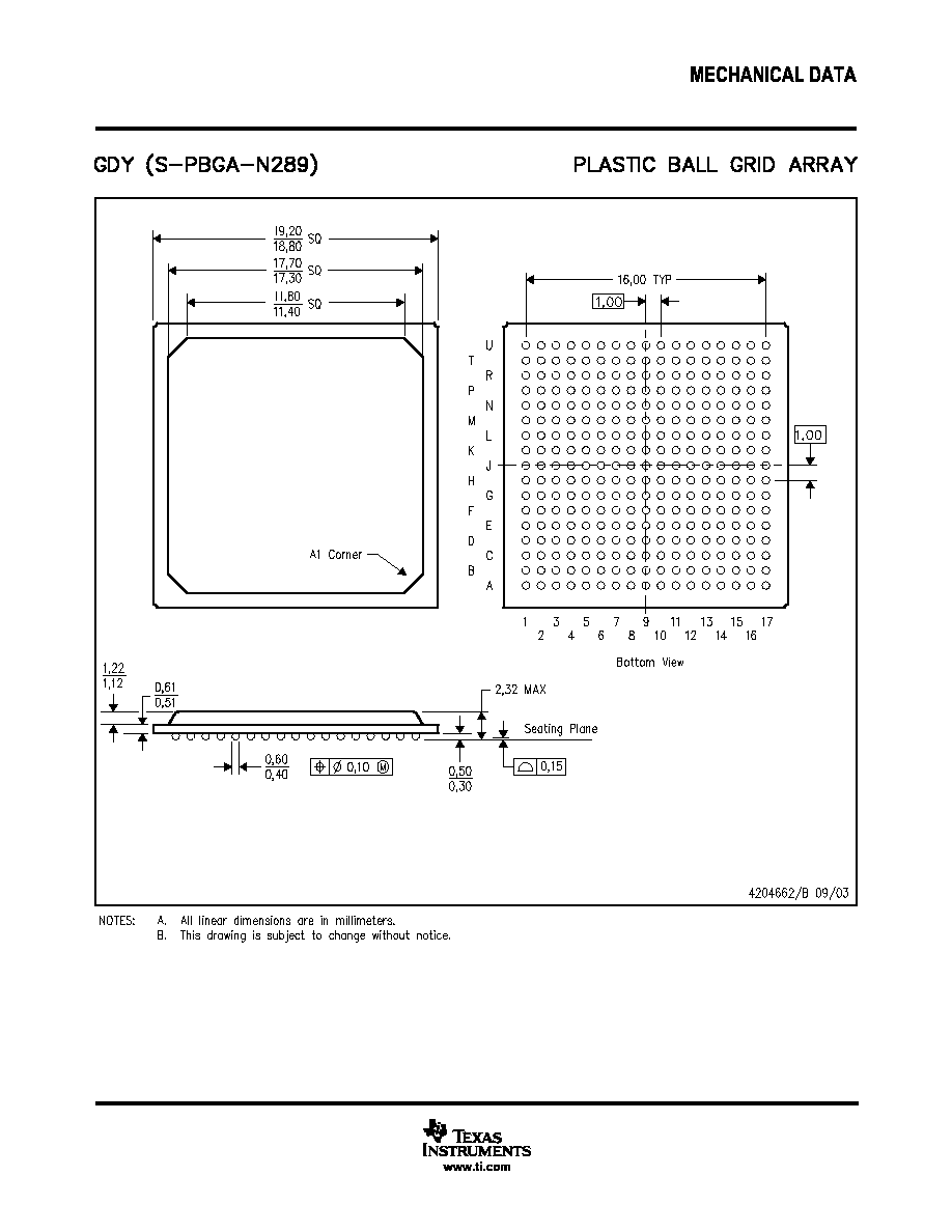
conjunction with Table 2-1 to locate signal names and ball grid numbers. GDY BGA ball numbers in
Figure 2-2 are read from left-to-right, top-to-bottom.
A
1
2
B
4
3
6
5
8
7
10
9
12
11
14
13
16
15
17
C
D
E
F
G
H
J
K
L
M
N
P
R
T
U
Bottom View
Figure 2-2. OMAP5910 GDY Package (Bottom View)
In Table 2-2, signals with multiplexed functions are separated with forward slashes as follows:
�
signal1/signal2/signal3 (for example, GPIO11/HDQ)
Signals which are associated with specific peripherals are denoted by using the peripheral name, followed
by a period, and then the signal name; as follows:
�
peripheral1.signal1 (for example, MCBSP1.DR)

Introduction
22
August 2002 - Revised August 2004
SPRS197D
Table 2-2. GDY BGA Terminal Assignments
GDY
BGA
BALL #
SIGNAL
GDY
BGA
BALL #
SIGNAL
GDY
BGA
BALL #
SIGNAL
GDY
BGA
BALL #
SIGNAL
A1
SDRAM.WE
A2
SDRAM.DQMU
A3
SDRAM.D[9]
A4
SDRAM.D[6]
A5
DV
DD4
A6
SDRAM.D[0]
A7
SDRAM.CLK
A8
SDRAM.A[9]
A9
SDRAM.A[5]
A10
SDRAM.A[1]
A11
LCD.AC
A12
LCD.PCLK
A13
LCD.P[9]
A14
DV
DD1
A15
LCD.P[6]
A16
LCD.P[3]
A17
KB.C[5]
B1
FLASH.A[1]
B2
SDRAM.DQML
B3
CV
DD1
B4
SDRAM.D[12]
B5
SDRAM.D[11]
B6
SDRAM.D[5]
B7
SDRAM.D[2]
B8
SDRAM.BA[0]
B9
SDRAM.A[11]
B10
SDRAM.A[2]
B11
SDRAM.A[0]
B12
LCD.P[13]
B13
LCD.P[11]
B14
LCD.P[7]
B15
LCD.P[4]
B16
LCD.P[0]
B17
KB.C[3]
C1
FLASH.A[3]
C2
FLASH.A[4]
C3
FLASH.RDY
C4
SDRAM.RAS
C5
SDRAM.D[14]
C6
SDRAM.D[10]
C7
SDRAM.D[3]
C8
SDRAM.A[12]
C9
SDRAM.BA[1]
C10
SDRAM.A[8]
C11
SDRAM.A[3]
C12
DV
DD1
C13
LCD.P[14]
C14
LCD.P[8]
C15
LCD.P[5]
C16
LCD.P[1]
C17
KB.C[0]
D1
DV
DD5
D2
FLASH.A[7]
D3
DV
DD4
D4
SDRAM.D[15]
D5
DV
DD4
D6
SDRAM.D[7]
D7
SDRAM.CKE
D8
DV
DD4
D9
SDRAM.A[6]
D10
SDRAM.A[4]
D11
LCD.VS
D12
LCD.P[15]
D13
KB.R[0]
D14
KB.R[1]
D15
LCD.P[2]
D16
KB.C[4]
D17
KB.R[4]
E1
FLASH.A[12]
E2
CV
DD
E3
FLASH.A[5]
E4
FLASH.A[6]
E5
V
SS
E6
SDRAM.D[8]
E7
SDRAM.D[1]
E8
CV
DD
E9
SDRAM.A[10]
E10
DV
DD4
E11
LCD.HS
E12
LCD.P[10]
E13
V
SS
E14
DV
DD1
E15
KB.C[2]
E16
KB.C[1]
E17
KB.R[3]
F1
DV
DD5
F2
FLASH.A[11]
F3
FLASH.A[9]
F4
FLASH.A[10]
F5
FLASH.A[8]
F6
V
SS
F7
SDRAM.D[4]
F8
SDRAM.CAS
F9
SDRAM.A[7]
F10
CV
DD3
F11
LCD.P[12]
F12
V
SS
F13
MCBSP1.CLKS
F14
PWRON_RESET
F15
KB.R[2]
F16
MCBSP1.FSX/
MCBSP1.DX
F17
MCBSP1.DX/
MCBSP1.FSX
G1
FLASH.A[16]
G2
FLASH.A[17]
G3
FLASH.A[14]
G4
FLASH.A[13]
G5
FLASH.A[15]
G6
FLASH.A[2]
G7
V
SS
G8
SDRAM.D[13]
G9
V
SS
G10
CV
DD3
G11
V
SS
G12
CAM.D[6]/
ETM.D[6]/
UWIRE.CS3
G13
CAM.EXCLK/
ETM.SYNC/
UWIRE.SDO
G14
CAM.D[7]/
ETM.D[7]/
UWIRE.CS0
G15
MCBSP1.CLKX
G16
MCBSP1.DR
G17
CAM.D[3]/
ETM.D[3]/
UART3.RX
H1
FLASH.ADV
H2
FLASH.A[20]
H3
FLASH.A[18]
H4
FLASH.A[19]
H5
FLASH.A[21]
H6
FLASH.A[22]
H7
DV
DD5
H8
V
SS
H9
V
SS
H10
V
SS
H11
CV
DD3
H12
UART3.RX/PWL/
UART2.RX
H13
DV
DD1
H14
CAM.D[1]/ETM.D[1]/
UART3.RTS
H15
CAM.LCLK/
ETM.CLK/
UWIRE.SCLK
H16
CAM.D[5]/
ETM.D[5]/
UWIRE.SDI
H17
CAM.D[2]/
ETM.D[2]/
UART3.CTS
J1
FLASH.BE[1]
J2
FLASH.CS0
J3
FLASH.A[24]
J4
FLASH.A[23]
J5
FLASH.BE[0]
J6
V
SS
J7
V
SS
J8
V
SS
See Section 5.6.1 and Section 5.6.2 for special V
SS
considerations with ocillator circuits.

Introduction
23
August 2002 - Revised August 2004
SPRS197D
Table 2-2. GDY BGA Terminal Assignments (Continued)
GDY
BGA
BALL #
SIGNAL
GDY
BGA
BALL #
SIGNAL
GDY
BGA
BALL #
SIGNAL
GDY
BGA
BALL #
SIGNAL
J9
V
SS
J10
V
SS
J11
V
SS
J12
V
SS
J13
UART3.TX/
PWT/
UART2.TX
J14
CAM.RSTZ/
ETM.PSTAT[0]/
UART2.RTS
J15
CAM.D[4]/
ETM.D[4]/
UART3.TX
J16
CAM.D[0]/
ETM.D[0]/
MPUIO12
J17
CAM.VS/
ETM.PSTAT[2]
K1
FLASH.CS1
K2
CV
DD4
K3
FLASH.D[1]
K4
FLASH.CLK
K5
FLASH.CS2/
FLASH.BAA
K6
DV
DD5
K7
CV
DD2
K8
V
SS
K9
V
SS
K10
V
SS
K11
CV
DD3
K12
GPIO3/
SPI.CS3/
MCBSP3.FSX/LED1
K13
GPIO6/
SPI.CS1/
MCBSP3.FSX
K14
GPIO13/
KB.R[5]
K15
CAM.HS/
ETM.PSTAT[1]/
UART2.CTS
K16
GPIO15/
KB.R[7]
K17
GPIO14/
KB.R[6]
L1
FLASH.CS3
L2
DV
DD5
L3
DV
DD5
L4
FLASH.D[2]
L5
FLASH.D[0]
L6
FLASH.D[3]
L7
V
SS
L8
CV
DD2
L9
V
SS
L10
BCLKREQ/
UART3.CTS/
UART1.DSR
L11
V
SS
L12
UWIRE.CS3/
KB.C[6]
L13
MPUIO5/
LOW_PWR
L14
GPIO4/
SPI.CS2/
MCBSP3.FSX
L15
GPIO12/
MCBSP3.FSX
L16
GPIO11/
HDQ
L17
GPIO7/
MMC.DAT2
M1
FLASH.D[4]
M2
FLASH.D[5]
M3
FLASH.D[11]
M4
FLASH.D[6]
M5
FLASH.D[7]
M6
V
SS
M7
UART2.RX/
USB2.VM
M8
GPIO9
M9
MMC.DAT1/
MPUIO7
M10
UART1.CTS
M11
RST_OUT
M12
V
SS
M13
UWIRE.SCLK/
KB.C[7]
M14
MPUIO1
M15
GPIO2/
SPI.CLK
M16
GPIO0/
SPI.RDY/
USB.VBUS
M17
GPIO1/
UART3.RTS
N1
FLASH.D[9]
N2
FLASH.D[13]
N3
FLASH.OE
N4
FLASH.D[8]
N5
V
SS
N6
UART2.CTS/
USB2.RCV/
GPIO7
N7
DV
DD3
N8
MCLKREQ/
EXT_MASTER_REQ
N9
CLK32K_IN
N10
CLK32K_OUT/
MPUIO0/
USB1.SPEED
N11
RSVD
N12
MCSI1.DOUT/
USB1.TXD
N13
V
SS
N14
I2C.SDA
N15
MPUIO4/
EXT_DMA_REQ1/
LED2
N16
DV
DD1
N17
MPUIO2/
EXT_DMA_REQ0
P1
FLASH.D[10]
P2
FLASH.WE
P3
OSC1_OUT
P4
USB.DM
P5
USB.DP
P6
MCBSP2.FSR/
GPIO12
P7
MPUIO3
P8
MCSI2.DIN/
USB2.VP
P9
DV
DD1
P10
CV
DD
P11
BCLK/
UART3.RTS/
UART1.DTR
P12
MPU_RST
P13
UART1.TX
P14
MCBSP3.CLKX/
USB1.TXEN
P15
I2C.SCL
See Section 5.6.1 and Section 5.6.2 for special V
SS
considerations with ocillator circuits.
Introduction
24
August 2002 - Revised August 2004
SPRS197D
Table 2-2. GDY BGA Terminal Assignments (Continued)
GDY
BGA
BALL #
SIGNAL
GDY
BGA
BALL #
SIGNAL
GDY
BGA
BALL #
SIGNAL
GDY
BGA
BALL #
SIGNAL
P16
UWIRE.SDO/
UART3.DTR/
UART1.DTR/
MCBSP3.DX
P17
UWIRE.SDI/
UART3.DSR/
UART1.DSR/
MCBSP3.DR
R1
FLASH.D[12]
R2
OSC1_IN
R3
FLASH.WP
R4
UART2.TX/
USB2.TXD
R5
MCBSP2.DX/
MCBSP2.DR
R6
MCBSP2.DR/
MCBSP2.DX
R7
MCSI2.SYNC/
GPIO7
R8
MMC.DAT2/
MPUIO11
R9
MMC.DAT3/
MPUIO6
R10
MCSI1.DIN/
USB1.RCV
R11
UART1.RX
R12
MPU_BOOT/
MCBSP3.DR/
USB1.SUSP
R13
TMS
R14
BFAIL/
EXT_FIQ
R15
CV
DDA
R16
UWIRE.CS0/
MCBSP3.CLKX
R17
EMU0
T1
FLASH.D[14]
T2
FLASH.RP
T3
USB.PUEN/
USB.CLKO
T4
UART2.BCLK
T5
MCBSP2.CLKR/
GPIO11
T6
MCBSP2.FSX
T7
MCSI2.DOUT/
USB2.TXEN
T8
MCSI2.CLK/
USB2.SUSP
T9
OSC32K_OUT
T10
OSC32K_IN
T11
MCSI1.SYNC/
USB1.VP
T12
DV
DD1
T13
EMU1
T14
TCK
T15
CLK32K_CTRL
T16
CONF
T17
CV
DD
U1
DV
DD5
U2
FLASH.D[15]
U3
DV
DD2
U4
UART2.RTS/
USB2.SE0/
MPUIO5
U5
MCBSP2.CLKX
U6
GPIO8
U7
MCLK
U8
MMC.CMD/SPI.DO
U9
MMC.DAT0/SPI.DI
U10
MMC.CLK
U11
MCSI1.CLK/
USB1.VM
U12
UART1.RTS
U13
RST_HOST_OUT/
MCBSP3.DX/
USB1.SE0
U14
STAT_VAL/
WKUP
U15
TRST
U16
TDO
U17
TDI
See Section 5.6.1 and Section 5.6.2 for special V
SS
considerations with ocillator circuits.
2.3
Terminal Characteristics and Multiplexing
Table 2-3 describes terminal characteristics and the signals multiplexed on each ball. The table column
headers are explained below:
�
SIGNAL NAME: The names of all the signals that are multiplexed on each ball.
�
TYPE: The terminal type when a particular signal is multiplexed on the terminal.
�
MUX CTRL SETTING: The register field that controls multiplexing on the terminal and the proper register
field setting necessary to select the signal to be multiplexed on the terminal. The reset values of these
register fields are indicated in bold type.
�
DESELECTED INPUT STATE: The logic level internally driven to the signal when it is not selected to be
multiplexed on the corresponding terminal.
�
PULLUP/PULLDN: Denotes the presence of an internal pullup or pulldown. Pullups and pulldowns can
be enabled or disabled via software.
�
BUFFER STRENGTH: Drive strength of the associated output buffer.
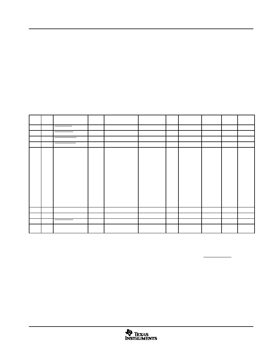
Introduction
25
August 2002 - Revised August 2004
SPRS197D
�
OTHER: Contains various terminal information, such as buffer type, boundary scan capability, and
gating/inhibit functionality. Certain terminals may be gated or 3-stated based on the state of other
terminals and/or software configuration register settings.
�
RESET STATE: The state of the terminal at reset.
�
SUPPLY: The voltage supply which powers the terminal's I/O buffers.
NOTE: Due to the extensive pin multiplexing options which are available on the OMAP5910
device, a software utility is available to ease the process of configuring the pins based on the
peripheral set required by a specific application. The 5910 OMAP Pin Configuration Utility is
currently available from Texas Instruments.
NOTE: Configuring two pins to the same input signal is not supported as it can yield unexpected
results. This can be easily avoided with proper software configuration.
Table 2-3. Terminal Characteristics and Multiplexing
GZG
BALL
GDY
BALL
SIGNAL NAME
TYPE
MUX CTRL
SETTING
DESELECTED
INPUT STATE
PU/
PD
�
BUFFER
STRENGTH
OTHER
�
RESET
STATE
#
SUPPLY
C3
A1
SDRAM.WE
O/Z
NA
NA
4 mA
A
1
DV
DD4
A2
C4
SDRAM.RAS
O/Z
NA
NA
4 mA
A
1
DV
DD4
D4
A2
SDRAM.DQMU
O/Z
NA
NA
4 mA
A
1
DV
DD4
B3
B2
SDRAM.DQML
O/Z
NA
NA
4 mA
A
1
DV
DD4
D5
C4
B4
D6
C5
H8
C6
B6
D7
C7
D8
B8
G8
C8
G9
B9
D4
C5
G8
B4
B5
C6
A3
E6
D6
A4
B6
F7
C7
B7
E7
A6
SDRAM.D[15:0]
I/O/Z
NA
NA
4 mA
E
0
DV
DD4
D9
D7
SDRAM.CKE
O/Z
NA
NA
4 mA
A
1
DV
DD4
C9
A7
SDRAM.CLK
I/O/Z
NA
NA
8 mA
E
LZ
DV
DD4
H9
F8
SDRAM.CAS
O/Z
NA
NA
4 mA
A
1
DV
DD4
D10
C10
C9
B8
SDRAM.BA[1:0]
O/Z
NA
NA
4 mA
A
0
DV
DD4
I = Input, O = Output, Z = High-Impedance
'regx' denotes the terminal multiplexing register that controls the specified terminal where regx = FUNC_MUX_CTRL_x
�
PD20 = 20-�A internal pulldown, PD100 = 100-�A pulldown, PU20 = 20-�A internal pullup, PU100 = 100-�A internal pullup
�
A = Standard LVCMOS input/output
G1 = Terminal may be gated by BFAIL
B = Fail-safe LVCMOS input/output
G2 = Terminal may be gated by GPIO9 and MPUIO3
C = USB transceiver input/output
G3 = Terminal may be gated by BFAIL and PWRON_RESET
D = I
2
C input/output buffers
H1 = Terminal may be 3-stated by BFAIL input
E = Fail-safe LVCMOS input and Standard LVCMOS output
J = Boundary-scannable terminal
F = analog oscillator terminals
#
Z = High-Impedance, LZ = Low-Impedance (pin is driven), 1 = Output driven high, 0 = Output driven low
||
UART1 signals can be multiplexed to this pin via additional multiplexing in the USB module.

Introduction
26
August 2002 - Revised August 2004
SPRS197D
Table 2-3. Terminal Characteristics and Multiplexing (Continued)
SUPPLY
RESET
STATE
#
OTHER
�
BUFFER
STRENGTH
PU/
PD
�
DESELECTED
INPUT STATE
MUX CTRL
SETTING
TYPE
SIGNAL NAME
GDY
BALL
GZG
BALL
G10
H10
C11
D11
G11
C12
D12
H11
C13
D13
G12
C14
B14
C8
B9
E9
A8
C10
F9
D9
A9
D10
C11
B10
A10
B11
SDRAM.A[12:0]
O/Z
NA
NA
4 mA
A
0
DV
DD4
D14
D11
LCD.VS
O
NA
NA
4 mA
J, A, G1
0
DV
DD1
H12
E11
LCD.HS
O
NA
NA
4 mA
J, A, G1
0
DV
DD1
B15
A11
LCD.AC
O
NA
NA
4 mA
J, A, G1
0
DV
DD1
C15
A12
LCD.PCLK
O
NA
NA
4 mA
J, A, G1
0
DV
DD1
D15
C16
A17
G13
B17
C17
D16
D17
C18
B19
A20
H13
G14
C19
B21
D18
D12
C13
B12
F11
B13
E12
A13
C14
B14
A15
C15
B15
A16
D15
C16
B16
LCD.P[15:0]
O
NA
NA
4 mA
J, A, G1
0
DV
DD1
C20
C21
E18
D19
D20
F18
A17
D16
B17
E15
E16
C17
KB.C[5:0]
O
NA
NA
4 mA
A, J
0
DV
DD1
E19
E20
H14
F19
G18
D17
E17
F15
D14
D13
KB.R[4:0]
I
NA
NA
A, J
input
DV
DD1
G19
F14
PWRON_RESET
I
NA
NA
B, J
input
DV
DD1
G20
F13
MCBSP1.CLKS
I
NA
NA
B, J
input
DV
DD1
G21
G15
MCBSP1.CLKX
I/O/Z
NA
NA
4 mA
J, B, G1
Z
DV
DD1
H15
F17
MCBSP1.FSX
I/O/Z
reg4[14:12] = 000
0
4 mA
J, B, G1
Z
DV
DD1
5
MCBSP1.DX
O
reg4[14:12] = 001
NA
J, , G
DD1
I = Input, O = Output, Z = High-Impedance
'regx' denotes the terminal multiplexing register that controls the specified terminal where regx = FUNC_MUX_CTRL_x
�
PD20 = 20-�A internal pulldown, PD100 = 100-�A pulldown, PU20 = 20-�A internal pullup, PU100 = 100-�A internal pullup
�
A = Standard LVCMOS input/output
G1 = Terminal may be gated by BFAIL
B = Fail-safe LVCMOS input/output
G2 = Terminal may be gated by GPIO9 and MPUIO3
C = USB transceiver input/output
G3 = Terminal may be gated by BFAIL and PWRON_RESET
D = I
2
C input/output buffers
H1 = Terminal may be 3-stated by BFAIL input
E = Fail-safe LVCMOS input and Standard LVCMOS output
J = Boundary-scannable terminal
F = analog oscillator terminals
#
Z = High-Impedance, LZ = Low-Impedance (pin is driven), 1 = Output driven high, 0 = Output driven low
||
UART1 signals can be multiplexed to this pin via additional multiplexing in the USB module.

Introduction
27
August 2002 - Revised August 2004
SPRS197D
Table 2-3. Terminal Characteristics and Multiplexing (Continued)
SUPPLY
RESET
STATE
#
OTHER
�
BUFFER
STRENGTH
PU/
PD
�
DESELECTED
INPUT STATE
MUX CTRL
SETTING
TYPE
SIGNAL NAME
GDY
BALL
GZG
BALL
H18
F16
MCBSP1.DX
O
reg4[17:15] = 000
NA
4 mA
J, B, G1
0
DV
DD1
8
6
MCBSP1.FSX
I/O/Z
reg4[17:15] = 001
0
J, , G
0
DD1
H20
G16
MCBSP1.DR
I
NA
NA
PD20
B , J
input
DV
DD1
H19
G13
CAM.EXCLK
O
reg4[23:21] = 000
NA
8 mA
J, A, G1
0
DV
DD1
9
G 3
ETM.SYNC
O
reg4[23:21] = 001
NA
8
J, , G
0
DD1
UWIRE.SDO
O
reg4[23:21] = 010
NA
J15
H15
CAM.LCLK
I
reg4[26:24] = 000
0
8 mA
B, J
input
DV
DD1
J 5
5
ETM.CLK
O
reg4[26:24] = 001
NA
8
, J
p
DD1
UWIRE.SCLK
O
reg4[26:24] = 010
NA
J18
G14
CAM.D[7]
I
reg4[29:27] = 000
NA
8 mA
B, J
input
DV
DD1
J 8
G
ETM.D[7]
O
reg4[29:27] = 001
NA
8
, J
p
DD1
UWIRE.CS0
O
reg4[29:27] = 010
NA
J19
G12
CAM.D[6]
I
reg5[2:0] = 000
NA
8 mA
B, J
input
DV
DD1
J 9
G
ETM.D[6]
O
reg5[2:0] = 001
NA
8
, J
p
DD1
UWIRE.CS3
O
reg5[2:0] = 010
NA
J14
H16
CAM.D[5]
I
reg5[5:3] = 000
NA
8 mA
B, J
input
DV
DD1
J
6
ETM.D[5]
O
reg5[5:3] = 001
NA
8
, J
p
DD1
UWIRE.SDI
I
reg5[5:3] = 010
NA
PD20
K18
J15
CAM.D[4]
I
reg5[8:6] = 000
NA
8 mA
B, J
input
DV
DD8
8
J 5
ETM.D[4]
O
reg5[8:6] = 001
NA
8
, J
p
DD8
UART3.TX
O
reg5[8:6] = 010
NA
K19
G17
CAM.D[3]
I
reg5[11:9] = 000
NA
8 mA
B, J
input
DV
DD1
9
G
ETM.D[3]
O
reg5[11:9] = 001
NA
8
, J
p
DD1
UART3.RX
I
reg5[11:9] = 010
NA
PD20
K15
H17
CAM.D[2]
I
reg5[14:12] = 000
NA
8 mA
B, J
input
DV
DD1
5
ETM.D[2]
O
reg5[14:12] = 001
NA
8
, J
p
DD1
UART3.CTS
I
reg5[14:12] = 010
NA
PD20
K14
H14
CAM.D[1]
I
reg5[17:15] = 000
NA
8 mA
B, J
input
DV
DD1
ETM.D[1]
O
reg5[17:15] = 001
NA
8
, J
p
DD1
UART3.RTS
O
reg5[17:15] = 010
NA
L19
J16
CAM.D[0]
I
reg5[20:18] = 000
NA
8 mA
B, J
input
DV
DD1
9
J 6
ETM.D[0]
O
reg5[20:18] = 001
NA
8
, J
p
DD1
MPUIO12
I/O/Z
reg5[20:18] = 010
NA
L18
J17
CAM.VS
I
reg5[23:21] = 000
NA
8 mA
B, J
input
DV
DD1
8
J
ETM.PSTAT[2]
O
reg5[23:21] = 001
NA
8
, J
p
DD1
L15
K15
CAM.HS
I
reg5[26:24] = 000
NA
8 mA
B, J
input
DV
DD1
5
5
ETM.PSTAT[1]
O
reg5[26:24] = 001
NA
8
, J
p
DD1
UART2.CTS
I
reg5[26:24] = 010
NA
PD20
I = Input, O = Output, Z = High-Impedance
'regx' denotes the terminal multiplexing register that controls the specified terminal where regx = FUNC_MUX_CTRL_x
�
PD20 = 20-�A internal pulldown, PD100 = 100-�A pulldown, PU20 = 20-�A internal pullup, PU100 = 100-�A internal pullup
�
A = Standard LVCMOS input/output
G1 = Terminal may be gated by BFAIL
B = Fail-safe LVCMOS input/output
G2 = Terminal may be gated by GPIO9 and MPUIO3
C = USB transceiver input/output
G3 = Terminal may be gated by BFAIL and PWRON_RESET
D = I
2
C input/output buffers
H1 = Terminal may be 3-stated by BFAIL input
E = Fail-safe LVCMOS input and Standard LVCMOS output
J = Boundary-scannable terminal
F = analog oscillator terminals
#
Z = High-Impedance, LZ = Low-Impedance (pin is driven), 1 = Output driven high, 0 = Output driven low
||
UART1 signals can be multiplexed to this pin via additional multiplexing in the USB module.

Introduction
28
August 2002 - Revised August 2004
SPRS197D
Table 2-3. Terminal Characteristics and Multiplexing (Continued)
SUPPLY
RESET
STATE
#
OTHER
�
BUFFER
STRENGTH
PU/
PD
�
DESELECTED
INPUT STATE
MUX CTRL
SETTING
TYPE
SIGNAL NAME
GDY
BALL
GZG
BALL
M19
J14
CAM.RSTZ
O
reg5[29:27] = 000
NA
8 mA
J, B, G1
0
DV
DD1
9
J
ETM.PSTAT[0]
O
reg5[29:27] = 001
NA
8
J, , G
0
DD1
UART2.RTS
O
reg5[29:27] = 010
NA
M18
J13
pin forced to drive low
O
reg6[2:0] = 000
NA
4 mA
J, A, G1
0
DV
DD1
8
J 3
UART3.TX
O
reg6[2:0] = 001
NA
J, , G
0
DD1
PWT
O
reg6[2:0] = 010
NA
IRQ_OBS
O
reg6[2:0] = 011
NA
UART2.TX
O
reg6[2:0] = 100
NA
L14
H12
UART3.RX
I
reg6[5:3] = 000
1
4 mA
B, J
input
DV
DD1
PWL
O
reg6[5:3] = 001
NA
, J
p
DD1
DMA_REQ_OBS
O
reg6[5:3] = 010
NA
UART2.RX
I
reg6[5:3] = 011
NA
M20
K16
GPIO15
I/O/Z
reg6[8:6] = 000
NA
PD20
4 mA
J, B, G1
input
DV
DD1
KB.R[7]
I
reg6[8:6] = 001
1
N21
K17
GPIO14
I/O/Z
reg6[11:9] = 000
NA
PD20
4 mA
J, B, G1
input
DV
DD1
KB.R[6]
I
reg6[11:9] = 001
1
J, , G
p
DD1
N19
GPIO13
I/O/Z
reg6[14:12] = 000
NA
PD20
4 mA
J, B, G1
input
DV
DD1
9
KB.R[5]
I
reg6[14:12] = 001
1
J, , G
p
DD1
N18
L15
GPIO12
I/O/Z
reg6[17:15] = 000
NA
PD20
4 mA
J, B, G1
input
DV
DD1
8
5
MCBSP3.FSX
I/O/Z
reg6[17:15] = 001
0
PD20
J, , G
p
DD1
N20
L16
GPIO11
I/O/Z
reg6[20:18] = 000
NA
PD20
4 mA
J, B, G1
input
DV
DD1
0
6
HDQ
I/O
reg6[20:18] = 001
NA
PD20
J, , G
p
DD1
M15
L17
GPIO7
I/O/Z
reg6[23:21] = 000
NA
PD20
4 mA
J, B, G1
input
DV
DD1
5
MMC.DAT2
I/O/Z
reg6[23:21] = 001
1
J, , G
p
DD1
P19
K13
GPIO6
I/O/Z
reg6[26:24] = 000
NA
PD20
4 mA
J, B, G1
input
DV
DD1
9
3
SPI.CS1
O
reg6[26:24] = 001
NA
J, , G
p
DD1
MCBSP3.FSX
I/O/Z
reg6[26:24] = 010
NA
PD20
P20
L14
GPIO4
I/O/Z
reg6[29:27] = 000
NA
PD20
4 mA
J, B, G1
input
DV
DD1
0
SPI.CS2
O
reg6[29:27] = 001
NA
J, , G
p
DD1
MCBSP3.FSX
I/O/Z
reg6[29:27] = 010
NA
PD20
P18
K12
GPIO3
I/O/Z
reg7[2:0] = 000
NA
PD20
4 mA
J, B, G1
input
DV
DD1
8
SPI.CS3
O
reg7[2:0] = 001
NA
J, , G
p
DD1
MCBSP3.FSX
I/O/Z
reg7[2:0] = 010
NA
PD20
LED1
O
reg7[2:0] = 011
NA
M14
M15
GPIO2
I/O/Z
reg7[5:3] = 000
NA
PD20
4 mA
J, B, G1
input
DV
DD1
5
SPI.CLK
O
reg7[5:3] = 001
NA
J, , G
p
DD1
I = Input, O = Output, Z = High-Impedance
'regx' denotes the terminal multiplexing register that controls the specified terminal where regx = FUNC_MUX_CTRL_x
�
PD20 = 20-�A internal pulldown, PD100 = 100-�A pulldown, PU20 = 20-�A internal pullup, PU100 = 100-�A internal pullup
�
A = Standard LVCMOS input/output
G1 = Terminal may be gated by BFAIL
B = Fail-safe LVCMOS input/output
G2 = Terminal may be gated by GPIO9 and MPUIO3
C = USB transceiver input/output
G3 = Terminal may be gated by BFAIL and PWRON_RESET
D = I
2
C input/output buffers
H1 = Terminal may be 3-stated by BFAIL input
E = Fail-safe LVCMOS input and Standard LVCMOS output
J = Boundary-scannable terminal
F = analog oscillator terminals
#
Z = High-Impedance, LZ = Low-Impedance (pin is driven), 1 = Output driven high, 0 = Output driven low
||
UART1 signals can be multiplexed to this pin via additional multiplexing in the USB module.
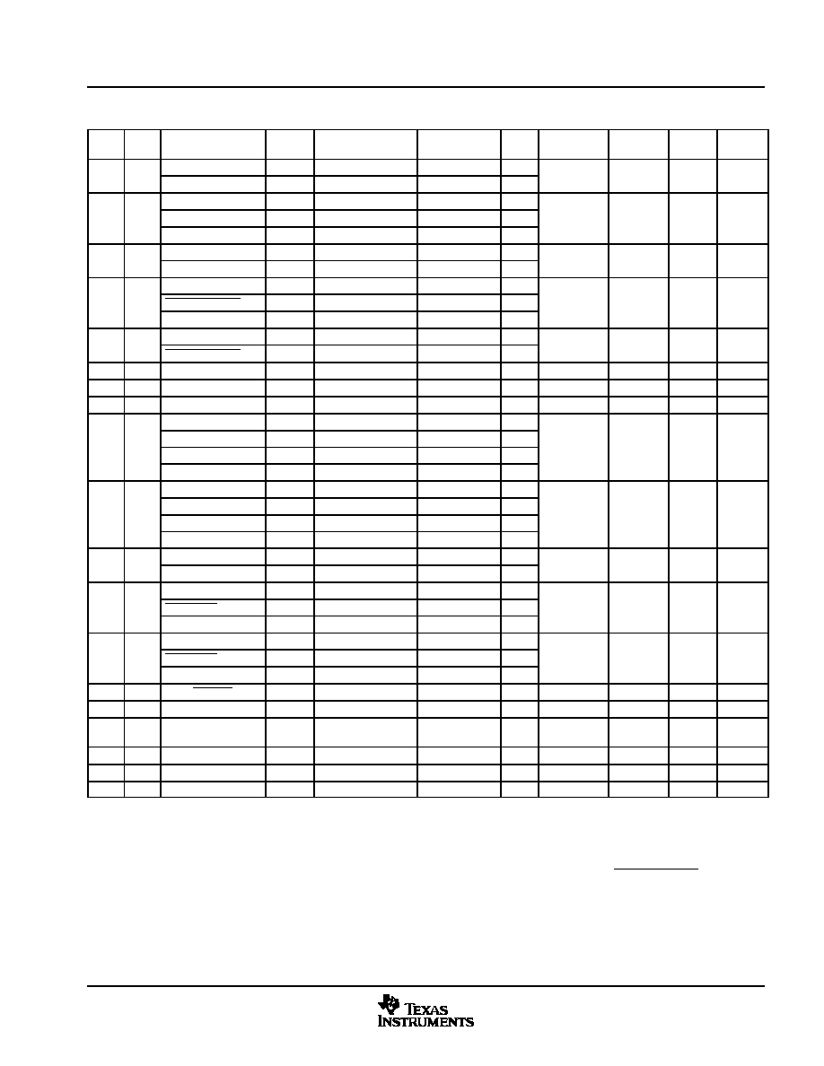
Introduction
29
August 2002 - Revised August 2004
SPRS197D
Table 2-3. Terminal Characteristics and Multiplexing (Continued)
SUPPLY
RESET
STATE
#
OTHER
�
BUFFER
STRENGTH
PU/
PD
�
DESELECTED
INPUT STATE
MUX CTRL
SETTING
TYPE
SIGNAL NAME
GDY
BALL
GZG
BALL
R19
M17
GPIO1
I/O/Z
reg7[8:6] = 000
NA
PD20
4 mA
J, B, G1
input
DV
DD1
9
UART3.RTS
O
reg7[8:6] = 001
NA
J, , G
p
DD1
R18
M16
GPIO0
I/O/Z
reg7[11:9] = 000
NA
PD20
4 mA
J, B, G1
input
DV
DD1
8
6
SPI.RDY
I
reg7[11:9] = 001
NA
J, , G
p
DD1
USB.VBUS
I
reg7[11:9] = 010
0
PD20
T20
L13
MPUIO5
I/O/Z
reg7[14:12] = 000
NA
PD20
4 mA
J, B, G1
input
DV
DD1
0
3
LOW_PWR
O
reg7[14:12] = 001
NA
J, , G
p
DD1
T19
N15
MPUIO4
I/O/Z
reg7[17:15] = 000
NA
PD20
4 mA
J, B, G1
input
DV
DD1
9
5
EXT_DMA_REQ1
I
reg7[17:15] = 001
NA
J, , G
p
DD1
LED2
O
reg7[17:15] = 010
NA
N15
N17
MPUIO2
I/O/Z
reg7[20:18] = 000
NA
PD20
4 mA
J, B, G1
input
DV
DD1
5
EXT_DMA_REQ0
I
reg7[20:18] = 001
NA
J, , G
p
DD1
U19
M14
MPUIO1
I/O/Z
NA
NA
4 mA
B, J
input
DV
DD1
T18
P15
I2C.SCL
I/O/Z
NA
NA
6 mA
J, D, H1
Z
DV
DD1
V20
N14
I2C.SDA
I/O/Z
NA
NA
6 mA
J, D, H1
Z
DV
DD1
U18
P17
UWIRE.SDI
I
reg8[2:0] = 000
NA
PD20
4 mA
B, J
input
DV
DD1
U 8
UART3.DSR
I
reg8[2:0] = 001
1
PD20
, J
p
DD1
UART1.DSR
I
reg8[2:0] = 010
1
PD20
MCBSP3.DR
I
reg8[2:0] = 011
NA
PD20
W21
P16
UWIRE.SDO
O
reg8[5:3] = 000
NA
4 mA
J, A, G1
0
DV
DD1
6
UART3.DTR
O
reg8[5:3] = 001
NA
J, , G
0
DD1
UART1.DTR
O
reg8[5:3] = 010
NA
MCBSP3.DX
O
reg8[5:3] = 011
NA
V19
M13
UWIRE.SCLK
O
reg8[8:6] = 000
NA
4 mA
J, A, G1
0
DV
DD1
9
3
KB.C[7]
O
reg8[8:6] = 001
NA
J, , G
0
DD1
N14
R16
pin forced to high-z
Z
reg8[11:9] = 000
NA
4 mA
J, A
Z
DV
DD1
6
UWIRE.CS0
O
reg8[11:9] = 001
NA
J,
DD1
MCBSP3.CLKX
I/O/Z
reg8[11:9] = 010
NA
P15
L12
pin forced to high-z
Z
reg8[14:12] = 000
NA
4 mA
J, A
Z
DV
DD1
5
UWIRE.CS3
O
reg8[14:12] = 001
NA
J,
DD1
KB.C[6]
O
reg8[14:12] = 010
NA
W19
R14
BFAIL/EXT_FIQ
I
NA
NA
J, B
input
DV
DD1
AA20
T15
CLK32K_CTRL
I
NA
NA
J, B
input
DV
DD1
V18
T16
CONF
I
NA
NA
PD10
0
A
input
DV
DD1
Y19
U17
TDI
I
NA
NA
PD20
B
input
DV
DD1
AA19
U16
TDO
O
NA
NA
4 mA
A
0
DV
DD1
V17
R13
TMS
I
NA
NA
PD20
B
input
DV
DD1
I = Input, O = Output, Z = High-Impedance
'regx' denotes the terminal multiplexing register that controls the specified terminal where regx = FUNC_MUX_CTRL_x
�
PD20 = 20-�A internal pulldown, PD100 = 100-�A pulldown, PU20 = 20-�A internal pullup, PU100 = 100-�A internal pullup
�
A = Standard LVCMOS input/output
G1 = Terminal may be gated by BFAIL
B = Fail-safe LVCMOS input/output
G2 = Terminal may be gated by GPIO9 and MPUIO3
C = USB transceiver input/output
G3 = Terminal may be gated by BFAIL and PWRON_RESET
D = I
2
C input/output buffers
H1 = Terminal may be 3-stated by BFAIL input
E = Fail-safe LVCMOS input and Standard LVCMOS output
J = Boundary-scannable terminal
F = analog oscillator terminals
#
Z = High-Impedance, LZ = Low-Impedance (pin is driven), 1 = Output driven high, 0 = Output driven low
||
UART1 signals can be multiplexed to this pin via additional multiplexing in the USB module.

Introduction
30
August 2002 - Revised August 2004
SPRS197D
Table 2-3. Terminal Characteristics and Multiplexing (Continued)
SUPPLY
RESET
STATE
#
OTHER
�
BUFFER
STRENGTH
PU/
PD
�
DESELECTED
INPUT STATE
MUX CTRL
SETTING
TYPE
SIGNAL NAME
GDY
BALL
GZG
BALL
W18
T14
TCK
I
NA
NA
PD20
B
input
DV
DD1
Y18
U15
TRST
I
NA
NA
PD10
0
B
input
DV
DD1
V16
R17
EMU0
I/O/Z
NA
NA
PU10
0
2 mA
B
Z
DV
DD1
W17
T13
EMU1
I/O/Z
NA
NA
PU10
0
2 mA
B
Z
DV
DD1
Y17
U14
STAT_VAL/WKUP
I
NA
NA
A
input
DV
DD1
AA17
R12
MPU_BOOT
I
reg8[29:27] = 000
NA
PD20
4 mA
J, B
input
DV
DD1
MCBSP3_DR
I
reg8[29:27] = 001
NA
PD20
J,
p
DD1
USB1_SUSP
O
reg8[29:27] = 010
NA
P14
U13
RST_HOST_OUT
O
reg9[2:0] = 000
NA
4 mA
J, A, G1
0
DV
DD1
U 3
MCBSP3.DX
O
reg9[2:0] = 001
NA
J, , G
0
DD1
USB1.SE0
O
reg9[2:0] = 010
NA
W16
P14
pin forced to high-z
Z
reg9[5:3] = 000
NA
PD20
4 mA
J, A, G1
Z
DV
DD1
6
MCBSP3.CLKX
I/O/Z
reg9[5:3] = 001
NA
PD20
J, , G
DD1
USB1.TXEN
O
reg9[5:3] = 010
NA
V15
P12
MPU_RST
I
NA
NA
J, B
input
DV
DD1
W15
M11
RST_OUT
O
NA
NA
4 mA
J, A
0
DV
DD1
AA15
U12
pin forced to drive low
O
reg9[14:12] = 000
NA
2 mA
J, A, G1
0
DV
DD1
5
U
UART1.RTS
O
reg9[14:12] = 001
NA
J, , G
0
DD1
R14
M10
UART1.CTS
I
NA
NA
PD20
J, B
input
DV
DD1
V14
R11
UART1.RX
I
NA
NA
PD20
J, B
input
DV
DD1
Y14
P13
pin forced to drive low
O
reg9[23:21] = 000
NA
2 mA
J, A, G1
0
DV
DD1
3
UART1.TX
O
reg9[23:21] = 001
NA
J, , G
0
DD1
W14
N12
MCSI1.DOUT
O
reg9[26:24] = 000
NA
2 mA
J, A, G1,
H1
0
DV
DD1
USB1.TXD
O
reg9[26:24] = 001
NA
J, , G ,
H1
0
DD1
UART1.TX
O
reg9[26:24] = 001
||
NA
R13
L10
BCLKREQ
I
reg9[29:27] = 000
0
PD20
J, B
input
DV
DD1
3
0
UART3.CTS
I
reg9[29:27] = 001
0
PD20
J,
p
DD1
UART1.DSR
I
reg9[29:27] = 010
1
PD20
Y13
P11
BCLK
O
regA[2:0] = 000
NA
4 mA
J, A, G1
0
DV
DD1
3
UART3.RTS
O
regA[2:0] = 001
NA
J, , G
0
DD1
UART1.DTR
O
regA[2:0] = 010
NA
V13
T11
MCSI1.SYNC
I/O/Z
regA[5:3] = 000
0
PD20
2 mA
J, B, G1
input
DV
DD1
3
USB1.VP
I
regA[5:3] = 001
NA
PD20
J, , G
p
DD1
I = Input, O = Output, Z = High-Impedance
'regx' denotes the terminal multiplexing register that controls the specified terminal where regx = FUNC_MUX_CTRL_x
�
PD20 = 20-�A internal pulldown, PD100 = 100-�A pulldown, PU20 = 20-�A internal pullup, PU100 = 100-�A internal pullup
�
A = Standard LVCMOS input/output
G1 = Terminal may be gated by BFAIL
B = Fail-safe LVCMOS input/output
G2 = Terminal may be gated by GPIO9 and MPUIO3
C = USB transceiver input/output
G3 = Terminal may be gated by BFAIL and PWRON_RESET
D = I
2
C input/output buffers
H1 = Terminal may be 3-stated by BFAIL input
E = Fail-safe LVCMOS input and Standard LVCMOS output
J = Boundary-scannable terminal
F = analog oscillator terminals
#
Z = High-Impedance, LZ = Low-Impedance (pin is driven), 1 = Output driven high, 0 = Output driven low
||
UART1 signals can be multiplexed to this pin via additional multiplexing in the USB module.

Introduction
31
August 2002 - Revised August 2004
SPRS197D
Table 2-3. Terminal Characteristics and Multiplexing (Continued)
SUPPLY
RESET
STATE
#
OTHER
�
BUFFER
STRENGTH
PU/
PD
�
DESELECTED
INPUT STATE
MUX CTRL
SETTING
TYPE
SIGNAL NAME
GDY
BALL
GZG
BALL
AA13
U11
MCSI1.CLK
I/O/Z
regA[8:6] = 000
0
PD20
2 mA
J, B, G1
input
DV
DD1
3
U
USB1.VM
I
regA[8:6] = 001
0
PD20
J, , G
p
DD1
UART1.RX
I
regA[8:6] = 001
||
0
PD20
W13
R10
MCSI1.DIN
I
regA[11:9] = 000
NA
PD20
J, B
input
DV
DD1
3
0
USB1.RCV
I
regA[11:9] = 001
0
PD20
J,
p
DD1
UART1.CTS
I
regA[11:9] = 001
||
0
PD20
Y12
N10
CLK32K_OUT
O
regA[14:12] = 000
NA
8 mA
J, A
LZ
DV
DD1
0
MPUIO0
I/O/Z
regA[14:12] = 001
NA
8
J,
DD1
USB1.SPEED
O
regA[14:12] = 010
NA
P13
N9
CLK32K_IN
I
NA
NA
J, B
input
DV
DD1
W12
T10
OSC32K_IN
-
NA
NA
F
NA
NA
R12
T9
OSC32K_OUT
-
NA
NA
F
NA
NA
W11
R9
MMC.DAT3
I/O/Z
regD[14:12] = 000
1
PU20
4 mA
J B G1
input
DV
DD1
9
Reserved
NA
regD[14:12] = 001
NA
J, B, G1
p
DD1
MPUIO6
I/O/Z
regD[14:12] = 010
NA
PU20
V11
U10
MMC.CLK
O
NA
NA
4 mA
J, A, G1
0
DV
DD1
R11
U9
MMC.DAT0/SPI.DI
I/O/Z
NA
NA
PU20
4 mA
J, B, G1
input
DV
DD1
W10
R8
MMC.DAT2
I/O/Z
regA[20:18] = 000
1
PU20
4 mA
J, B, G1
input
DV
DD1
0
8
pin forced to hi-z
Z
regA[20:18] = 001
NA
J, , G
p
DD1
MPUIO11
I/O/Z
regA[20:18] = 010
NA
PU20
V10
M9
MMC.DAT1
I/O/Z
regA[26:24] = 000
1
PU20
4 mA
J, B, G1
input
DV
DD1
0
9
Reserved
NA
regA[26:24] = 001
NA
J, , G
p
DD1
MPUIO7
I/O/Z
regA[26:24] = 010
NA
PU20
P11
U8
MMC.CMD/SPI.DO
I/O/Z
NA
NA
PU10
0
4 mA
J, B, G1
input
DV
DD1
Y10
T8
MCSI2.CLK
I/O/Z
regB[5:3] = 000
0
PD20
4 mA
J, E
input
DV
DD3
0
8
USB2.SUSP
O
regB[5:3] = 001
NA
J,
p
DD3
AA9
P8
MCSI2.DIN
I
regB[8:6] = 000
NA
PD20
J, B
input
DV
DD3
9
8
USB2.VP
I
regB[8:6] = 001
0
PD20
J,
p
DD3
W9
T7
MCSI2.DOUT
O
regB[11:9] = 000
NA
4 mA
J, A, G2
0
DV
DD3
9
USB2.TXEN
O
regB[11:9] = 001
NA
J, , G
0
DD3
V9
R7
MCSI2.SYNC
I/O/Z
regB[14:12] = 000
0
PD20
4 mA
J, E
input
DV
DD3
9
GPIO7
I/O/Z
regB[14:12] = 001
NA
PD20
J,
p
DD3
Y9
U7
MCLK
O
NA
NA
4 mA
J, A, G1
0
DV
DD3
R10
N8
MCLKREQ
I
regB[20:18] = 000
0
PD20
4 mA
J, E
input
DV
DD3
0
8
EXT_MASTER_REQ
O
regB[20:18] = 001
NA
J,
p
DD3
W8
M8
GPIO9
I/O/Z
NA
NA
PD20
4 mA
J, E, G3
input
DV
DD3
Y8
U6
GPIO8
I/O/Z
NA
NA
PD20
4 mA
J, E, G3
input
DV
DD3
I = Input, O = Output, Z = High-Impedance
'regx' denotes the terminal multiplexing register that controls the specified terminal where regx = FUNC_MUX_CTRL_x
�
PD20 = 20-�A internal pulldown, PD100 = 100-�A pulldown, PU20 = 20-�A internal pullup, PU100 = 100-�A internal pullup
�
A = Standard LVCMOS input/output
G1 = Terminal may be gated by BFAIL
B = Fail-safe LVCMOS input/output
G2 = Terminal may be gated by GPIO9 and MPUIO3
C = USB transceiver input/output
G3 = Terminal may be gated by BFAIL and PWRON_RESET
D = I
2
C input/output buffers
H1 = Terminal may be 3-stated by BFAIL input
E = Fail-safe LVCMOS input and Standard LVCMOS output
J = Boundary-scannable terminal
F = analog oscillator terminals
#
Z = High-Impedance, LZ = Low-Impedance (pin is driven), 1 = Output driven high, 0 = Output driven low
||
UART1 signals can be multiplexed to this pin via additional multiplexing in the USB module.

Introduction
32
August 2002 - Revised August 2004
SPRS197D
Table 2-3. Terminal Characteristics and Multiplexing (Continued)
SUPPLY
RESET
STATE
#
OTHER
�
BUFFER
STRENGTH
PU/
PD
�
DESELECTED
INPUT STATE
MUX CTRL
SETTING
TYPE
SIGNAL NAME
GDY
BALL
GZG
BALL
V8
P7
MPUIO3
I/O/Z
NA
NA
PD20
4 mA
J, E, G1
input
DV
DD3
P10
R6
MCBSP2.DR
I
regC[2:0] = 000
NA
PD20
4 mA
J, B, G2
input
DV
DD3
0
6
MCBSP2.DX
O
regC[2:0] = 001
NA
J, , G
p
DD3
W7
T6
MCBSP2.FSX
I/O/Z
NA
0
PD20
4 mA
J, E, G2
input
DV
DD3
V7
T5
MCBSP2.CLKR
I/O/Z
regC[8:6] = 000
0
4 mA
J, E
Z
DV
DD3
5
GPIO11
I/O/Z
regC[8:6] = 001
NA
PD20
J,
DD3
Y6
U5
MCBSP2.CLKX
I/O/Z
NA
NA
PD20
4 mA
J, E, G2
input
DV
DD3
W6
P6
MCBSP2.FSR
I/O/Z
regC[14:12] = 000
0
4 mA
J, E
Z
DV
DD3
6
6
GPIO12
I/O/Z
regC[14:12] = 001
NA
PD20
J,
DD3
AA5
R5
MCBSP2.DX
O
regC[17:15] = 000
NA
4 mA
J, E, G2
0
DV
DD3
5
5
MCBSP2.DR
I
regC[17:15] = 001
NA
PD20
J, , G
0
DD3
R9
M7
UART2.RX
I
regC[20:18] = 000
1
PD20
4 mA
J, B
input
DV
DD3
9
USB2.VM
I
regC[20:18] = 001
0
PD20
J,
p
DD3
Y5
N6
UART2.CTS
I
regC[23:21] = 000
1
PD20
4 mA
J, B
input
DV
DD3
5
6
USB2.RCV
I
regC[23:21] = 001
0
PD20
J, B
p
DD3
GPIO7
I/O/Z
regC[23:21] = 010
NA
PD20
J, E
W5
U4
pin forced to drive low
O
regC[26:24] = 000
NA
4 mA
J, E, G2
0
DV
DD3
5
U
UART2.RTS
O
regC[26:24] = 001
NA
J, , G
0
DD3
USB2.SE0
O
regC[26:24] = 010
NA
MPUIO5
I/O/Z
regC[26:24] = 011
NA
V6
R4
pin forced to drive low
O
regC[29:27] = 000
NA
4 mA
J, A, G2
0
DV
DD3
6
UART2.TX
O
regC[29:27] = 001
NA
J, , G
0
DD3
USB2.TXD
O
regC[29:27] = 010
NA
Y4
T4
UART2.BCLK
O
NA
NA
4 mA
J, A, G2
0
DV
DD3
W4
T3
USB.PUEN
O
regD[5:3] = 000
NA
8 mA
J, B, G1
0
DV
DD2
3
USB.CLKO
O
regD[5:3] = 001
NA
8
J, , G
0
DD2
P9
P5
USB.DP
I/O/Z
NA
NA
18.3 mA
C
Z
DV
DD2
R8
P4
USB.DM
I/O/Z
NA
NA
18.3 mA
C
Z
DV
DD2
Y2
R2
OSC1_IN
-
NA
NA
F
NA
NA
W3
P3
OSC1_OUT
-
NA
NA
F
NA
NA
V4
R3
FLASH.WP
O/Z
NA
NA
4 mA
A
0
DV
DD5
W2
P2
FLASH.WE
O/Z
NA
NA
4 mA
A
1
DV
DD5
W1
T2
FLASH.RP
O/Z
NA
NA
4 mA
A
0
DV
DD5
U4
N3
FLASH.OE
O/Z
NA
NA
4 mA
A
1
DV
DD5
I = Input, O = Output, Z = High-Impedance
'regx' denotes the terminal multiplexing register that controls the specified terminal where regx = FUNC_MUX_CTRL_x
�
PD20 = 20-�A internal pulldown, PD100 = 100-�A pulldown, PU20 = 20-�A internal pullup, PU100 = 100-�A internal pullup
�
A = Standard LVCMOS input/output
G1 = Terminal may be gated by BFAIL
B = Fail-safe LVCMOS input/output
G2 = Terminal may be gated by GPIO9 and MPUIO3
C = USB transceiver input/output
G3 = Terminal may be gated by BFAIL and PWRON_RESET
D = I
2
C input/output buffers
H1 = Terminal may be 3-stated by BFAIL input
E = Fail-safe LVCMOS input and Standard LVCMOS output
J = Boundary-scannable terminal
F = analog oscillator terminals
#
Z = High-Impedance, LZ = Low-Impedance (pin is driven), 1 = Output driven high, 0 = Output driven low
||
UART1 signals can be multiplexed to this pin via additional multiplexing in the USB module.

Introduction
33
August 2002 - Revised August 2004
SPRS197D
Table 2-3. Terminal Characteristics and Multiplexing (Continued)
SUPPLY
RESET
STATE
#
OTHER
�
BUFFER
STRENGTH
PU/
PD
�
DESELECTED
INPUT STATE
MUX CTRL
SETTING
TYPE
SIGNAL NAME
GDY
BALL
GZG
BALL
V3
T4
U3
U1
P8
T3
T2
R4
R3
R2
P7
P4
P2
N7
N2
N4
U2
T1
N2
R1
M3
P1
N1
N4
M5
M4
M2
M1
L6
L4
K3
L5
FLASH.D[15:0]
I/O/Z
NA
NA
4 mA
E
0
DV
DD5
N3
K4
FLASH.CLK
O/Z
NA
NA
8 mA
E, G1, H2
0
DV
DD5
N8
L1
FLASH.CS3
O/Z
NA
NA
4 mA
A
1
DV
DD5
M4
K5
FLASH.CS2
O/Z
regD[8:6] = 000
NA
4 mA
A
1
DV
DD5
5
FLASH.BAA
O/Z
regD[8:6] = 001
NA
DD5
M3
K1
FLASH.CS1
O/Z
NA
NA
4 mA
A
1
DV
DD5
M7
J2
FLASH.CS0
O/Z
NA
NA
4 mA
A
1
DV
DD5
M8
L3
J1
J5
FLASH.BE[1:0]
O/Z
NA
NA
4 mA
A
0
DV
DD5
L4
H1
FLASH.ADV
O/Z
NA
NA
4 mA
A
1
DV
DD5
L7
K3
K4
L8
J1
J3
J4
J2
K7
H3
H4
K8
G2
G3
G4
F3
J7
E3
F4
D2
E4
C1
D3
J8
J3
J4
H6
H5
H2
H4
H3
G2
G1
G5
G3
G4
E1
F2
F4
F3
F5
D2
E4
E3
C2
C1
G6
B1
FLASH.A[24:1]
O/Z
NA
NA
4 mA
A, G1
0
DV
DD5
H7
C3
FLASH.RDY
I
NA
NA
B
input
DV
DD5
E5
N11
RSVD
NA
NA
NA
NA
NA
I = Input, O = Output, Z = High-Impedance
'regx' denotes the terminal multiplexing register that controls the specified terminal where regx = FUNC_MUX_CTRL_x
�
PD20 = 20-�A internal pulldown, PD100 = 100-�A pulldown, PU20 = 20-�A internal pullup, PU100 = 100-�A internal pullup
�
A = Standard LVCMOS input/output
G1 = Terminal may be gated by BFAIL
B = Fail-safe LVCMOS input/output
G2 = Terminal may be gated by GPIO9 and MPUIO3
C = USB transceiver input/output
G3 = Terminal may be gated by BFAIL and PWRON_RESET
D = I
2
C input/output buffers
H1 = Terminal may be 3-stated by BFAIL input
E = Fail-safe LVCMOS input and Standard LVCMOS output
J = Boundary-scannable terminal
F = analog oscillator terminals
#
Z = High-Impedance, LZ = Low-Impedance (pin is driven), 1 = Output driven high, 0 = Output driven low
||
UART1 signals can be multiplexed to this pin via additional multiplexing in the USB module.

Introduction
34
August 2002 - Revised August 2004
SPRS197D
2.4
Signal Description
Table 2-4 provides a description of the signals on OMAP5910. Many signals are available on multiple pins
depending upon the software configuration of the pin multiplexing options. Ball numbers which are italicized
indicate the default pin muxings at reset. Ball numbers for busses are listed from MSB to LSB (left to right,
top to bottom).
Table 2-4. Signal Description
SIGNAL
GZG
BALL
GDY
BALL
DESCRIPTION
TYPE
EMIFF SDRAM Interface
SDRAM.WE
C3
A1
SDRAM write enable. SDRAM.WE is active (low) during writes, DCAB, and MRS
commands to SDRAM memory.
O/Z
SDRAM.RAS
A2
C4
SDRAM row address strobe. SDRAM.RAS is active (low) during ACTV, DCAB,
REFR, and MRS commands to SDRAM memory.
O/Z
SDRAM.DQMU
D4
A2
SDRAM upper data mask. Active-low data mask for the upper byte of the SDRAM
data bus (SDRAM.D[15:8]). The data mask outputs allow for both 16-bit-wide and
8-bit-wide accesses to SDRAM memories.
O/Z
SDRAM.DQML
B3
B2
SDRAM lower data mask. Active-low data mask for the lower byte of the SDRAM
data bus (SDRAM.D[7:0]). The data mask outputs allow for both 16-bit-wide and
8-bit-wide accesses to SDRAM memories.
O/Z
SDRAM.D[15:0]
D5,
C4,
B4,
D6,
C5,
H8,
C6,
B6,
D7,
C7,
D8,
B8,
G8,
C8,
G9,
B9
D4,
C5,
G8,
B4,
B5,
C6,
A3,
E6,
D6,
A4,
B6,
F7,
C7,
B7,
D7,
A6
SDRAM data bus. SDRAM.D[15:0] provides data exchange between the Traffic
Controller and SDRAM memory.
I/O/Z
SDRAM.CKE
D9
D7
SDRAM clock enable. Active-high output which enables the SDRAM clock during
normal operation; SDRAM.CKE is driven inactive to put the memory into
low-power mode.
O/Z
SDRAM.CLK
C9
A7
SDRAM clock. Clock for synchronization SDRAM memory commands/accesses.
To minimize voltage undershoot and overshoot effects, it is recommended to place
a series resistor (typically ~33 ) close to the SDRAM.CLK driver pin.
SDRAM.CLK can also be configured as an input to monitor skew control.
I/O/Z
SDRAM.CAS
H9
F8
SDRAM column address strobe. SDRAM.CAS is active (low) during reads, writes,
and the REFR and MRS commands to SDRAM memory.
O/Z
SDRAM.BA[1:0]
D10,
C10
C9,
B8
SDRAM bank address bus. Provides the bank address to SDRAM memories.
O/Z
I = Input, O = Output, Z = High-Impedance
All core voltage supplies should be tied to the same voltage level (within 0.3 V). During system prototyping phases, it may be useful to maintain
a capability for independent measurement of core supply currents to facilitate power optimization experiments.
�
See Sections 5.6.1 and 5.6.2 for special V
SS
considerations with oscillator circuits.

Introduction
35
August 2002 - Revised August 2004
SPRS197D
Table 2-4. Signal Description (Continued)
SIGNAL
TYPE
DESCRIPTION
GDY
BALL
GZG
BALL
EMIFF SDRAM Interface (Continued)
SDRAM.A[12:0]
G10,
H10,
C11,
D11,
G11,
C12,
D12,
H11,
C13,
D13,
G12,
C14,
B14
C8,
B9,
E9,
A8,
C10,
F9,
D9,
A9,
D10,
C11,
B10,
A10,
B11
SDRAM address bus. Provides row and column address information to the
SDRAM memory as well as MRS command data. SDRAM.A[10] also serves as a
control signal to define specific commands to SDRAM memory.
O/Z
EMIFS FLASH and Asynchronous Memory Interface
FLASH.WP
V4
R3
EMIFS write protect. Active-low output for hardware write protection feature on
standard memory devices.
O/Z
FLASH.WE
W2
P2
EMIFS write enable. Active-low write enable output for Flash or SRAM memories
or asynchronous devices.
O/Z
FLASH.RP
W1
T2
EMIFS power down or reset output (Intel flash devices)
O/Z
FLASH.OE
U4
N3
EMIFS output enable. Active-low output enable output for Flash or SRAM
memories or asynchronous devices.
O/Z
FLASH.D[15:0]
V3,
T4,
U3,
U1,
P8,
T3,
T2,
R4,
R3,
R2,
P7,
P4,
P2,
N7,
N2,
N4
U2,
T1,
N2,
R1,
M3,
P1,
N1,
N4,
M5,
M4,
M2,
M1,
L6,
L4,
K3,
L5
EMIFS data bus. Bidirectional 16-bit data bus used to transfer read and write data
during EMIFS accesses.
I/O/Z
FLASH.CLK
N3
K4
EMIFS clock. Clock output that is active during synchronous modes of EMIFS
operation for synchronous burst Flash memories.
O/Z
FLASH.CS3
N8
L1
EMIFS chip selects. Active-low chip-select outputs that become active when the
i
dd
i d
d d i
l h d i
E h hi l
d
d
O/Z
FLASH.CS2
M4
K5
p
p
p
appropriate address is decoded internal to the device. Each chip select decodes a
32M-byte region of memory space
/
FLASH.CS1
M3
K1
32M-byte region of memory space.
FLASH.CS0
M7
J2
FLASH.BE[1:0]
M8,
L3
J1,
J5
EMIFS byte enables. Active-low byte enable signals used to perform byte-wide
accesses to memories or devices that support byte enables.
O/Z
FLASH.ADV
L4
H1
EMIFS address valid. Active-low control signal used to indicate a valid address is
present on the FLASH.A[24:1] bus.
O/Z
FLASH.BAA
M4
K5
EMIFS burst advance acknowledge. Active-low control signal used with Advanced
Micro Devices burst Flash. FLASH.BAA is multiplexed with FLASH.CS2.
O/Z
I = Input, O = Output, Z = High-Impedance
All core voltage supplies should be tied to the same voltage level (within 0.3 V). During system prototyping phases, it may be useful to maintain
a capability for independent measurement of core supply currents to facilitate power optimization experiments.
�
See Sections 5.6.1 and 5.6.2 for special V
SS
considerations with oscillator circuits.
Advanced Micro Devices is a trademark of Advanced Micro Devices, Inc.
Intel is a registered trademark of Intel Corporation.

Introduction
36
August 2002 - Revised August 2004
SPRS197D
Table 2-4. Signal Description (Continued)
SIGNAL
TYPE
DESCRIPTION
GDY
BALL
GZG
BALL
EMIFS FLASH and Asynchronous Memory Interface (Continued)
FLASH.A[24:1]
L7,
K3,
K4,
L8,
J1,
J3,
J4,
J2,
K7,
H3,
H4,
K8,
G2,
G3,
G4,
F3,
J7,
E3,
F4,
D2,
E4,
C1,
D3,
J8
J3,
J4,
H6,
H5,
H2,
H4,
H3,
G2,
G1,
G5,
G3,
G4,
E1,
F2,
F4,
F3,
F5,
D2,
E4,
E3,
C2,
C1,
G6,
B1
EMIFS address bus. Address output bus for all EMIFS accesses. FLASH.A[24:1]
provides the upper 24 bits of a 25-bit byte address. The byte enables must be
used to implement 8-bit accesses.
O/Z
FLASH.RDY
H7
C3
EMIFS ready. Active-high ready input used to suspend the EMIFS interface when
the external memory or asynchronous device is not ready to continue the current
cycle. It is recommended that this pin should be pulled high externally and
unused. See the OMAP5910 Dual-Core Processor Silicon Errata (literature
number SPRZ016) for more details.
I
LCD Interface
LCD.VS
D14
D11
LCD vertical sync output. LCD.VS is the frame clock which signals the start of a
new frame of pixels to the LCD panel. In TFT mode, LCD.VS is the vertical
synchronization signal.
O
LCD.HS
H12
E11
LCD horizontal sync. LCD.HS is the line clock which signals the end of a line of
pixels to the LCD panel. In TFT mode, LCD.HS is the horizontal synchronization
signal.
O
LCD.AC
B15
A11
LCD AC-bias. LCD.AC is used to signal the LCD to switch the polarity of the row
and column power supplies to counteract charge buildup causing DC offset. In
TFT mode, LCD.AC is used as the output enable to latch LCD pixel data using the
pixel clock.
O
LCD.PCLK
C15
A12
LCD pixel clock output. Clock output provided to synchronize pixel data to the
LCD panel. In passive mode, LCD.PCLK only transitions when LCD.P[15:0] is
valid. In active mode, LCD.PCLK transitions continuously and LCD.AC is used as
the output enable when LCD.P[15:0] is valid.
O
I = Input, O = Output, Z = High-Impedance
All core voltage supplies should be tied to the same voltage level (within 0.3 V). During system prototyping phases, it may be useful to maintain
a capability for independent measurement of core supply currents to facilitate power optimization experiments.
�
See Sections 5.6.1 and 5.6.2 for special V
SS
considerations with oscillator circuits.

Introduction
37
August 2002 - Revised August 2004
SPRS197D
Table 2-4. Signal Description (Continued)
SIGNAL
TYPE
DESCRIPTION
GDY
BALL
GZG
BALL
LCD Interface (Continued)
LCD.P[15:0]
D15,
C16,
A17,
G13,
B17,
C17,
D16,
D17,
C18,
B19,
A20,
H13,
G14,
C19,
B21,
D18
D12,
C13,
B12,
F11,
B13,
E12,
A13,
C14,
B14,
A15,
C15,
B15,
A16,
D15,
C16,
B16
LCD pixel data bus. Pixel data is transferred on this output bus to LCD panel.
O
Keyboard Matrix Interface
KB.C[7:0]
V19,
P15,
C20,
C21,
E18,
D19,
D20,
F18
M13,
L12,
A17,
D16,
B17,
E15,
E16,
C17
Keyboard matrix column outputs. KB.Cx column outputs are used in conjunction
with the KB.Rx row inputs to implement a 6x5 or 8x8 keyboard matrix.
O
KB.R[7:0]
M20,
N21,
N19,
E19,
E20,
H14,
F19,
G18
K16,
K17,
K14,
D17,
E17,
F15,
D14,
D13
Keyboard matrix row inputs. KB.Rx row inputs are used in conjunction with the
KB.Cx column outputs to implement a 6x5 or 8x8 keyboard matrix.
I
Multichannel Buffered Serial Ports (McBSPs)
MCBSP1.CLKS
G20
F13
McBSP1 clock source. Provides external clock reference for use with transmitter
or reciever. CLKS is only present on McBSP1.
I
MCBSP1.CLKX
G21
G15
McBSP transmit clock. Serial shift clock reference for the transmitter. CLKX is
ll M BSP I h
f M BSP1 d M BSP3 h l k i
I/O/Z
MCBSP2.CLKX
Y6
U5
present on all McBSPs. In the case of McBSP1 and McBSP3, the clock input to
the McBSP receiver may also be provided on this terminal via an internal
/ /
MCBSP3.CLKX
W16,
N14
P14,
R16
the McBSP receiver may also be provided on this terminal via an internal
loop-back connection between the transmitter and receiver clocks.
MCBSP1.FSX
H15,
H18
F17,
F16
McBSP transmit frame sync. Frame synchronization for transmitter. FSX is
present on all McBSPs. In the case of McBSP1 and McBSP3, the frame sync
i
t t th M BSP
i
l b
id d thi t
i l i i t
l
I/O/Z
MCBSP2.FSX
W7
T6
p
,
y
input to the McBSP receiver may also be provided on this terminal via an internal
loop-back connection between the transmitter and receiver frame syncs
MCBSP3.FSX
N18,
P18,
P19,
P20
L15,
K12,
K13,
L14
loop-back connection between the transmitter and receiver frame syncs.
I = Input, O = Output, Z = High-Impedance
All core voltage supplies should be tied to the same voltage level (within 0.3 V). During system prototyping phases, it may be useful to maintain
a capability for independent measurement of core supply currents to facilitate power optimization experiments.
�
See Sections 5.6.1 and 5.6.2 for special V
SS
considerations with oscillator circuits.

Introduction
38
August 2002 - Revised August 2004
SPRS197D
Table 2-4. Signal Description (Continued)
SIGNAL
TYPE
DESCRIPTION
GDY
BALL
GZG
BALL
Multichannel Buffered Serial Ports (McBSPs) (Continued)
MCBSP1.DX
H18,
H15
F16,
F17
McBSP transmit data. Serial transmit data output. DX is present on all McBSPs.
O
MCBSP2.DX
AA5,
P10
R5,
R6
MCBSP3.DX
P14,
W21
U13,
P16
MCBSP2.CLKR
V7
T5
McBSP2 receive clock. Serial shift clock reference for the receiver. CLKR is only
present on McBSP2.
I/O/Z
MCBSP2.FSR
W6
P6
McBSP2 receive frame sync. Frame synchronization for the receiver. FSR is only
present on McBSP2.
I/O/Z
MCBSP1.DR
H20
G16
McBSP receive data. Serial receive data input. DR is present on all McBSPs.
I
MCBSP2.DR
P10,
AA5
R6,
R5
p
p
MCBSP3.DR
AA17,
U18
R12,
P17
Camera Interface
CAM.EXCLK
H19
G13
Camera interface external clock. Output clock used to provide a timing reference
to a camera sensor.
O
CAM.LCLK
J15
H15
Camera interface line clock. Input clock to provide external timing reference from
camera sensor logic.
I
CAM.VS
L18
J17
Camera interface vertical sync. Vertical synchronization input from external
camera sensor.
I
CAM.HS
L15
K15
Camera interface horizontal sync. Horizontal synchronization input from external
camera sensor.
I
CAM.D[7:0]
J18,
J19,
J14,
K18,
K19,
K15,
K14,
L19
G14,
G12,
H16,
J15,
G17,
H17,
H14,
J16
Camera interface data. Data input bus to receive image data from an external
camera sensor.
I
CAM.RSTZ
M19
J14
Camera interface reset. Reset output used to reset or Initialize external camera
sensor logic.
O
ETM9 Trace Macro Interface
ETM.CLK
J15
H15
ETM9 Trace Clock. Clock output for standard ETM9 test/debug equipment.
O
ETM.SYNC
H19
G13
ETM9 Trace Synchronization. Trace Sync output for standard ETM9 test/debug
equipment.
O
ETM.D[7:0]
J18,
J19,
J14,
K18,
K19,
K15,
K14,
L19
G14,
G12,
H16,
J15,
G17,
H17,
H14,
J16
ETM9 Trace Packet data. Trace Packet outputs for standard ETM9 test/debug
equipment.
O
I = Input, O = Output, Z = High-Impedance
All core voltage supplies should be tied to the same voltage level (within 0.3 V). During system prototyping phases, it may be useful to maintain
a capability for independent measurement of core supply currents to facilitate power optimization experiments.
�
See Sections 5.6.1 and 5.6.2 for special V
SS
considerations with oscillator circuits.

Introduction
39
August 2002 - Revised August 2004
SPRS197D
Table 2-4. Signal Description (Continued)
SIGNAL
TYPE
DESCRIPTION
GDY
BALL
GZG
BALL
ETM9 Trace Macro Interface (Continued)
ETM.PSTAT[2:0]
L18,
L15,
M19
J17,
K15,
J14
ETM9 Trace Pipe State 2-0. Pipeline status outputs for standard ETM9 test/debug
equipment.
O
MICROWIRE Interface
UWIRE.SCLK
V19,
J15
M13,
H15
MICROWIRE serial clock. This pin drives a clock to a MICROWIRE device. The
active edge is software configurable.
O
UWIRE.SDO
W21,
H19
P16,
G13
MICROWIRE serial data out. Write data is transferred to a MICROWIRE device on
this pin.
O
UWIRE.SDI
U18,
J14
P17,
H16
MICROWIRE serial data in. Read data is transferred from a MICROWIRE device
on this pin.
I
UWIRE.CS0
N14,
J18
R16,
G14
MICROWIRE chip select 0. The CS0 output selects a single MICROWIRE device
(configurable as active high or active low).
O
UWIRE.CS3
P15,
J19
L12,
G12
MICROWIRE chip select 3. The CS3 output selects a single MICROWIRE device
(configurable as active high or active low).
O
HDQ/1-Wire Interface
HDQ
N20
L16
HDQ/1-wire interface. HDQ optionally implements one of two serial protocols:
HDQ or 1-Wire.
I/O
General-Purpose I/O (GPIO) and MPU I/O (MPUIO)
GPIO15
M20
K16
Shared General-Purpose I/O. Each GPIO pin can be used by either the DSP core
h MPU
C
l f
h GPIO i b
h
i l
d b
I/O/Z
GPIO14
N21
K17
p
/
p
y
or the MPU core. Control of each GPIO pin between the two cores is selected by
the MPU via control registers Each GPIO pin may also be configured to cause an
/ /
GPIO13
N19
K14
the MPU via control registers. Each GPIO pin may also be configured to cause an
interrupt to its respective core processor.
GPIO12
N18,
W6
L15,
P6
interrupt to its respective core processor.
GPIO5 and GPIO10 are not available on the OMAP5910 device
GPIO11
N20,
V7
L16,
T5
GPIO5 and GPIO10 are not available on the OMAP5910 device.
GPIO9
W8
M8
GPIO8
Y8
U6
GPIO7
M15,
Y5,
V9
L17,
N6,
R7
GPIO6
P19
K13
GPIO4
P20
L14
GPIO3
P18
K12
GPIO2
M14
M15
GPIO1
R19
M17
GPIO0
R18
M16
I = Input, O = Output, Z = High-Impedance
All core voltage supplies should be tied to the same voltage level (within 0.3 V). During system prototyping phases, it may be useful to maintain
a capability for independent measurement of core supply currents to facilitate power optimization experiments.
�
See Sections 5.6.1 and 5.6.2 for special V
SS
considerations with oscillator circuits.
Introduction
40
August 2002 - Revised August 2004
SPRS197D
Table 2-4. Signal Description (Continued)
SIGNAL
TYPE
DESCRIPTION
GDY
BALL
GZG
BALL
General-Purpose I/O (GPIO) and MPU I/O (MPUIO) (Continued)
MPUIO12
L19
J16
MPU General-Purpose I/O. MPUIO pins may only be used by the MPU core.
I/O/Z
MPUIO11
W10
R8
p
/
p
y
y
y
MPUIO8 MPUIO9 AND MPUIO10 are not available on the OMAP5910 device
/ /
MPUIO7
V10
M9
MPUIO8, MPUIO9, AND MPUIO10 are not available on the OMAP5910 device.
MPUIO6
W11
R9
MPUIO5
T20,
W5
L13,
U4
MPUIO4
T19
N15
MPUIO3
V8
P7
MPUIO2
N15
N17
MPUIO1
U19
M14
MPUIO0
Y12
N10
Pulse-Width Tone and Pulse-Width Light Interface
PWT
M18
J13
Pulse Width Tone output. The PWT output pin provides a modulated output for use
with an external buzzer.
O
PWL
L14
H12
Pulse Width Light output. The PWL output pin provides a pseudo-random
modulated voltage output used for LCD or keypad backlighting.
O
Multimedia Card/Secure Digital Interface (MMC/SD)
MMC.CLK
V11
U10
MMC/SD clock. Clock output to the MMC/SD card.
O
MMC.CMD
P11
U8
MMC/SD command output. MMC/SD commands are transferred to/from this pin.
I/O/Z
MMC.DAT3
W11
R9
SD card data bit 3. Data bit 3 used in 4-bit Secure Digital mode.
I/O/Z
MMC.DAT2
W10,
M15
R8,
L17
SD card data bit 2. Data bit 2 used in 4-bit Secure Digital mode.
I/O/Z
MMC.DAT1
V10
M9
SD card data bit 1. Data bit 1 used in 4 -bit Secure Digital mode.
I/O/Z
MMC.DAT0
R11
U9
MMC/SD dat0 input. MMC.DAT0 functions as data bit 0 during MMC and Secure
Digital operation. The pin functions as the data input in generic SPI mode.
I/O/Z
I = Input, O = Output, Z = High-Impedance
All core voltage supplies should be tied to the same voltage level (within 0.3 V). During system prototyping phases, it may be useful to maintain
a capability for independent measurement of core supply currents to facilitate power optimization experiments.
�
See Sections 5.6.1 and 5.6.2 for special V
SS
considerations with oscillator circuits.
Introduction
41
August 2002 - Revised August 2004
SPRS197D
Table 2-4. Signal Description (Continued)
SIGNAL
TYPE
DESCRIPTION
GDY
BALL
GZG
BALL
Universal Asynchronous Receiver/Transmitter Interfaces
UART1.TX
Y14
P13
UART transmit. Transmit data output. TX is present on all UARTs. On UART3, the
TX i i
l
h TXIR f
i d i SIR
d
i
O
UART2.TX
V6,
M18
R4,
J13
p
p
,
TX pin implements the TXIR function during SIR mode operation.
UART3.TX
M18,
K18
J13,
J15
UART1.RX
V14
R11
UART receive. Receive data input. RX is present on all UARTs. On UART3, the
RX i i
l
h RXIR f
i d i SIR
d
i
I
UART2.RX
R9,
L14
M7,
H12
p
p
,
RX pin implements the RXIR function during SIR mode operation.
UART3.RX
L14,
K19
H12,
G17
UART1.CTS
R14
M10
UART clear-to-send. CTS is present on all UARTs.
I
UART2.CTS
Y5,
L15
N6,
K15
p
UART3.CTS
R13,
K15
L10,
H17
UART1.RTS
AA15
U12
UART request-to-send. RTS is present on all UARTs. On UART3 in IrDA mode,
hi i i SD MODE
O
UART2.RTS
W5,
M19
U4,
J14
q
p
,
this pin is SD_MODE.
UART3.RTS
Y13,
R19,
K14
P11,
M17,
H14
UART1.DTR
W21,
Y13
P16,
P11
UART data-terminal-ready. DTR is only present on UART1 and UART3.
O
UART3.DTR
W21
P16
UART1.DSR
U18,
R13
P17,
L10
UART data-set-ready. DSR is only present on UART1 and UART3.
I
UART3.DSR
U18
P17
UART2.BCLK
Y4
T4
UART baud clock output. A clock of 16x of the UART2 baud rate is driven onto this
pin. This feature is only implemented on UART2.
O
Inter-Integrated Circuit Master and Slave Interface
I2C.SCL
T18
P15
I
2
C serial clock. I2C.SCL provides the timing reference for I
2
C transfers.
I/O/Z
I2C.SDA
V20
N14
I
2
C serial data. I2C.SDA provides control and data for I
2
C transfers.
I/O/Z
LED Pulse Generator Interface
LED1
P18
K12
LED Pulse Generator output 1. LED1 produces a static or pulsing output used to
drive an external LED indicator.
O
LED2
T19
N15
LED Pulse Generator output 2. LED2 produces a static or pulsing output used to
drive an external LED indicator.
O
Multichannel Serial Interfaces (MCSIs)
MCSI1.CLK
AA13
U11
MCSI clock. Multichannel Serial Interface clock reference. The clock can be driven
i
d
l l k
b d i
hi i
l i l
d
I/O/Z
MCSI2.CLK
Y10
T8
in master mode or an external clock may be driven on this signal in slave mode.
/ /
MCSI1.SYNC
V13
T11
MCSI sync. Multichannel Serial Interface frame synchronization signal. The frame
sync can be driven in master mode or an external clock may be driven on this
I/O/Z
MCSI2.SYNC
V9
R7
sync can be driven in master mode or an external clock may be driven on this
signal in slave mode. MCSIx.SYNC may be configured as an active-low or
active-high sync.
I = Input, O = Output, Z = High-Impedance
All core voltage supplies should be tied to the same voltage level (within 0.3 V). During system prototyping phases, it may be useful to maintain
a capability for independent measurement of core supply currents to facilitate power optimization experiments.
�
See Sections 5.6.1 and 5.6.2 for special V
SS
considerations with oscillator circuits.
Introduction
42
August 2002 - Revised August 2004
SPRS197D
Table 2-4. Signal Description (Continued)
SIGNAL
TYPE
DESCRIPTION
GDY
BALL
GZG
BALL
Multichannel Serial Interfaces (MCSIs) (Continued)
MCSI1.DIN
W13
R10
MCSI data in. Multichannel Serial Interface data input pin.
I
MCSI2.DIN
AA9
P8
p p
MCSI1.DOUT
W14
N12
MCSI data out. Multichannel Serial Interface data output pin.
O
MCSI2.DOUT
W9
T7
p p
USB (Integrated Transceiver Interface, can be used with Host or Function)
USB.DP
P9
P5
USB internal transceiver D+. The positive side of the integrated USB transceiver's
differential bus. A series resistor of 27 (5% tolerance) is required on the
USB.DP pin.
I/O/Z
USB.DM
R8
P4
USB internal transceiver D-. The negative side of the integrated USB
transceiver's differential bus. A series resistor of 27 (5% tolerance) is required
on the USB.DM pin.
I/O/Z
USB Pin Group 1 and 2 (Utilizing External Transceivers, can be used with Host or Function)
USB1.TXEN
W16
P14
USB transmit enable. Driven active (low) when the USB host or Function
i h
l i d i i d
h USB b i h TXD
O
USB2.TXEN
W9
T7
(
)
peripheral is driving data onto the USB bus via the TXD output.
USB1.TXD
W14
N12
USB transmit data. Single-ended logic output used to transmit data to the transmit
input of an external USB transceiver. USBx.TXD may also be used for
O
USB2.TXD
V6
R4
input of an external USB transceiver. USBx.TXD may also be used for
transceiverless connection between OMAP5910 and another transceiverless USB
device.
USB1.VP
V13
T11
USB vplus data. Single-ended input used to monitor the logical state of the D+ line
of the USB bus USBx VP should be driven by an external USB transceiver based
I
USB2.VP
AA9
P8
of the USB bus. USBx.VP should be driven by an external USB transceiver based
on the state of D+.
USB1.VM
AA13
U11
USB vminus data. Single-ended input used to monitor the logical state of the D-
line of the USB bus USBx VM should be driven by an external USB transceiver
I
USB2.VM
R9
M7
line of the USB bus. USBx.VM should be driven by an external USB transceiver
based on the state of D-.
USB1.RCV
W13
R10
USB receive data. Single-ended logic input used to receive data from the receive
output of an external USB transceiver. USBx.RCV may also be used for
I
USB2.RCV
Y5
N6
output of an external USB transceiver. USBx.RCV may also be used for
transceiverless connection between OMAP5910 and another transceiverless USB
device.
USB1.SUSP
AA17
R12
USB bus segment suspend control. Active-high output indicates detection of IDLE
condition on the USB bus for greater than 5 ms USBx SUSP is implemented on
O
USB2.SUSP
Y10
T8
condition on the USB bus for greater than 5 ms. USBx.SUSP is implemented on
both USB ports 1 and 2.
USB1.SE0
P14
U13
USB single-ended zero. Active-high output indicates detection of the single-ended
h USB b
USB SE i i
l
d f b h USB
d
O
USB2.SE0
W5
U4
g
g
p
g
zero state on the USB bus. USBx.SE0 is implemented for both USB ports 1 and 2.
USB1.SPEED
Y12
N10
USB 1 bus segment speed control. Static control output used by the external
transceiver to determine whether USB port 1 is operating in full-speed or
low-speed mode. USB1.SPEED is only implemented on USB port 1.
O
I = Input, O = Output, Z = High-Impedance
All core voltage supplies should be tied to the same voltage level (within 0.3 V). During system prototyping phases, it may be useful to maintain
a capability for independent measurement of core supply currents to facilitate power optimization experiments.
�
See Sections 5.6.1 and 5.6.2 for special V
SS
considerations with oscillator circuits.

Introduction
43
August 2002 - Revised August 2004
SPRS197D
Table 2-4. Signal Description (Continued)
SIGNAL
TYPE
DESCRIPTION
GDY
BALL
GZG
BALL
USB Miscellaneous Signals
USB.CLKO
W4
T3
USB clock output. 6-MHz divided clock output of the internal USB DPLL provided
for reference. Common for all USB host and Function peripherals.
O
USB.PUEN
W4
T3
USB pullup enable. Control output used in conjunction with an external pullup
resistor to implement USB device connect and disconnect via software.
USB.PUEN is used with the USB Function peripheral.
O
USB.VBUS
R18
M16
USB voltage bus enable. USB.VBUS is used to provide a logic-high voltage level
which may be used to enable pullup resistors on the USB bus to indicate
connection or disconnection status of the OMAP5910 device as a USB Function
device.
I
JTAG/Emulation Interface
TCK
W18
T14
IEEE Standard 1149.1 test clock. TCK is normally a free-running clock signal with
a 50% duty cycle. The changes on the test access port (TAP) of input signals TDI
and TMS are clocked into the TAP controller, instruction register, or selected test
data register on the rising edge of TCK. Changes at the TAP output signal TDO
occur on the falling edge of TCK.
I
TDI
Y19
U17
IEEE Standard 1149.1 test data input. TDI is clocked into the selected register
(instruction or data) on the rising edge of TCK.
I
TDO
AA19
U16
IEEE Standard 1149.1 test data output. The contents of the selected register
(instruction or data) are shifted out of TDO on the falling edge of TCK. TDO is in
the high-impedance state except when the scanning of data is in progress.
O
TMS
V17
R13
IEEE Standard 1149.1 test mode select. This serial control input is clocked into
the TAP controller on the rising edge of TCK.
I
TRST
Y18
U15
IEEE Standard 1149.1 test reset. TRST, when high, gives the IEEE standard
1149.1 scan system control of the operations of the device. If TRST is not
connected, or driven low, the device operates in its functional mode, and the IEEE
standard 1149.1 signals are ignored.
I
EMU0
V16
R17
Emulation pin 0. When TRST is driven high, EMU0 is used as an interrupt to or
from the emulator system and is defined as input/output by way of the IEEE
standard 1149.1 scan system.
I/O
EMU1
W17
T13
Emulation pin 1. When TRST is driven high, EMU1 is used as an interrupt to or
from the emulator system and is defined as input/output by way of the IEEE
standard 1149.1 scan system.
I/O
Device Clock Pins
CLK32K_IN
P13
N9
32-kHz clock input. Digital CMOS 32-kHz clock input driven by an external
32-kHz oscillator if the internal 32-kHz oscillator is not used.
I
CLK32K_OUT
Y12
N10
32-kHz clock output. Clock output reflecting the internal 32-kHz clock.
O
CLK32K_CTRL
AA20
T15
32-kHz clock selection control input. CLK32K_CTRL selects whether or not the
internal 32-kHz oscillator is used or if the 32-kHz clock is to be provided externally
via the CLK32K_IN input. If CLK32K_CTRL is high, the 32-kHz internal oscillator
is used; if CLK32K_CTRL is low, the CMOS input CLK32K_IN is used as a 32-kHz
clock source.
I
OSC32K_IN
W12
T10
32-kHz crystal XI connection. Analog clock input to 32-kHz oscillator for use with
external crystal.
analog
OSC32K_OUT
R12
T9
32-kHz crystal XO connection. Analog output from 32-kHz oscillator for use with
external crystal.
analog
OSC1_IN
Y2
R2
Base crystal XI connection. Analog input to base oscillator for use with external
crystal or to be driven by external 12- or 13-MHz oscillator.
analog
I = Input, O = Output, Z = High-Impedance
All core voltage supplies should be tied to the same voltage level (within 0.3 V). During system prototyping phases, it may be useful to maintain
a capability for independent measurement of core supply currents to facilitate power optimization experiments.
�
See Sections 5.6.1 and 5.6.2 for special V
SS
considerations with oscillator circuits.
Introduction
44
August 2002 - Revised August 2004
SPRS197D
Table 2-4. Signal Description (Continued)
SIGNAL
TYPE
DESCRIPTION
GDY
BALL
GZG
BALL
Device Clock Pins (Continued)
OSC1_OUT
W3
P3
Base crystal XO connection. Analog output from base oscillator for use with
external 12- or 13-MHz crystal.
analog
MCLK
Y9
U7
M-Clock. General-purpose clock output which may be configured to run at 12 MHz
or 48 MHz. MCLK may be configured to drive constantly or only when the
MCLKREQ signal is asserted active high.
O
BCLK
Y13
P11
B-Clock. General purpose clock output which may be configured to run at
12 MHz. BCLK may be configured to drive constantly or only when the BCLKREQ
signal is asserted active high.
O
MCLKREQ
R10
N8
M-Clock Request. Active high request input which allows an external device to
request that MCLK be driven.
I
BCLKREQ
R13
L10
B-Clock Request. Active high request input which allows an external device to
request that BCLK be driven.
I
Reset Logic Pins
PWRON_RESET
G19
F14
Reset input to device. Active-low asynchronous reset input resets the entire
OMAP5910 device.
I
MPU_RST
V15
P12
MPU reset input. Active-low asynchronous reset input resets the MPU core.
I
RST_OUT
W15
M11
Reset output. Active-low output is asserted when MPUST is active (after
synchronization.)
O
Interrupts and Miscellaneous Control and Configuration Pins
MPU_BOOT
AA17
R12
MPU boot mode. When MPU_BOOT is low, the MPU boots from chip select 0 of
the EMIFS (Flash) interface. When MPU_BOOT is high, the MPU boots from chip
select 3 of EMIFS.
I
DMA_REQ_OBS
L14
H12
DMA request external observation output.
O
IRQ_OBS
M18
J13
IRQ external observation output.
O
EXT_DMA_REQ1
T19
N15
External DMA requests. EXT_DMA_REQ0 and EXT_DMA_REQ1 provide two
DMA request inputs which external devices may use to trigger System DMA
I
EXT_DMA_REQ0
N15
N17
DMA request inputs which external devices may use to trigger System DMA
transfers. The System DMA must be configured in software to respond to these
external requests.
BFAIL/EXT_FIQ
W19
R14
Battery power failure and external FIQ interrupt input. BFAIL/EXT_FIQ may be
used to gate certain input pins when battery power is low or failing. The pins which
may be gated are configured via software. This pin can also optionally be used as
an external FIQ interrupt source to the MPU. The function of this pin is
configurable via software.
I
EXT_MASTER_REQ
R10
N8
External master request. If the 12-MHz clock is provided by an external device
instead of using the on-chip oscillator, a high level on this output indicates to the
external device that the clock must be driven. A low level indicates that the
OMAP5910 device is in sleep mode and the 12-MHz clock is not necessary.
O
LOW_PWR
T20
L13
Low-power request output. This active-high output indicates that the OMAP5910
device is in a low-power sleep mode. During reset and functional modes,
LOW_PWR is driven low. This signal can be used to indicate a low-power state to
external power management devices in a system or it can be used as a chip
select to external SDRAM memory to minimize current consumption while the
SDRAM is in self-refresh and the OMAP5910 device is in sleep mode.
O
CONF
V18
T16
Configuration input. CONF selects reserved factory test modes. CONF should
always be pulled low during device operation.
I
I = Input, O = Output, Z = High-Impedance
All core voltage supplies should be tied to the same voltage level (within 0.3 V). During system prototyping phases, it may be useful to maintain
a capability for independent measurement of core supply currents to facilitate power optimization experiments.
�
See Sections 5.6.1 and 5.6.2 for special V
SS
considerations with oscillator circuits.

Introduction
45
August 2002 - Revised August 2004
SPRS197D
Table 2-4. Signal Description (Continued)
SIGNAL
TYPE
DESCRIPTION
GDY
BALL
GZG
BALL
Interrupts and Miscellaneous Control and Configuration Pins (Continued)
STAT_VAL/WKUP
Y17
U14
Static Valid / Chip wake-up input. STAT_VAL/WKUP is also sampled at reset to
select the MMC/SD port. If the MMC/SD peripheral is to be used, this pin must be
pulled high during reset. It is recommended that this pin be pulled high during
reset regardless of whether or not MMC/SD will be used.
I
RST_HOST_OUT
P14
U13
Reset Host output. A software controllable Reset or Shutdown output to an
external device.
O
RSVD
E5
N11
Reserved pin. This pin must be left unconnected.
-
Power Supplies
V
SS
�
A11,
A13,
A21,
B1,
B2,
B5,
B7,
B16,
B18,
E2,
F20,
G1,
J20,
K2,
K20,
N1,
R21,
U2,
U20,
V5,
V12,
W20,
Y3,
Y15,
AA1,
AA7,
AA21
G9,
H9,
N5,
H8,
G11,
M6,
L11,
K8,
J12,
J9,
G7,
E5,
J7,
J8,
J6,
J10,
K10,
H10,
F12,
L7,
F6,
L9,
K9,
M12,
E13,
J11,
N13
Ground. Common ground return for all core and I/O voltage supplies.
power
CV
DD
A9,
F2,
P12,
Y20
E8,
E2,
T17,
P10
Core supply voltage. Supplies power to OMAP5910 core logic and low-voltage
sections of I/O.
power
CV
DD1
A3
B3
Core Supply Voltage 1. Supplies power to the on-chip shared SRAM memory
(192k-Bytes).
power
CV
DD2
Y1,
AA3
K7,
L8
Core Supply Voltage 2. Supplies power to the MPU subsystem logic and memory.
power
CV
DD3
B13,
B20,
J21,
R20
F10,
G10,
H11,
K11
Core Supply Voltage 3. Supplies power to the DSP subsystem logic and memory.
power
CV
DD4
M2
K2
Core Supply Voltage 4. Supplies power to the DPLL which provides internal clocks
to the core and peripherals (excluding USB peripherals). NOTE: The voltage to
this supply pin should be kept as clean as possible to maximize performance.
power
I = Input, O = Output, Z = High-Impedance
All core voltage supplies should be tied to the same voltage level (within 0.3 V). During system prototyping phases, it may be useful to maintain
a capability for independent measurement of core supply currents to facilitate power optimization experiments.
�
See Sections 5.6.1 and 5.6.2 for special V
SS
considerations with oscillator circuits.

Introduction
46
August 2002 - Revised August 2004
SPRS197D
Table 2-4. Signal Description (Continued)
SIGNAL
TYPE
DESCRIPTION
GDY
BALL
GZG
BALL
Power Supplies (Continued)
CV
DDA
Y21
R15
Analog supply voltage. Supplies power to ULPD DPLL which provides an internal
clock to the USB peripherals. NOTE: The voltage to this supply pin should be kept
as clean as possible to maximize performance.
power
DV
DD1
A15,
A19,
E21,
L21,
U21,
AA11,
Y16
C12,
A14,
E14,
H13,
N16,
P9,
T12
I/O Supply Voltage 1. Supplies power to the majority of peripheral I/O buffers.
DV
DD1
may be connected in common with the other DV
DD
supplies if the same
operating voltage is desired.
power
DV
DD2
AA2
U3
I/O Supply Voltage 2. Supplies power to the internal USB transceiver buffers.
DV
DD2
may optionally be used for USB connect and disconnect detection by
connecting DV
DD2
to the power from the USB bus in the system. DV
DD2
may be
connected in common with the other DV
DD
supplies if the same operating voltage
is desired.
power
DV
DD3
Y7
N7
I/O Supply Voltage 3. Supplies power to the MCSI2 and McBSP2 peripheral I/O
buffers as well as GPIO[9:8] I/O buffers. The DV
DD3
supply may operate within a
high-voltage or low-voltage range (see Section 5.2 for operating conditions).
DV
DD3
may be connected in common with the other DV
DD
supplies if the same
operating voltage is desired.
power
DV
DD4
A1,
A5,
A7,
B10,
B12
D3,
D5,
A5,
D8,
E10
I/O Supply Voltage 4. Supplies power to the SDRAM interface I/O buffers. The
DV
DD4
supply may operate within a high-voltage or low-voltage range (see
Section 5.2 for operating conditions). DV
DD4
may be connected in common with
the other DV
DD
supplies if the same operating voltage is desired.
power
DV
DD5
C2,
E1,
H2,
L1,
P3,
R1,
V2
H7,
D1,
F1,
K6,
L2,
L3,
U1
I/O Supply Voltage 5. Supplies power to the FLASH interface I/O buffers. The
DV
DD5
supply may operate within a high-voltage or low-voltage range (see
Section 5.2 for operating conditions). DV
DD5
may be connected in common with
the other DV
DD
supplies if the same operating voltage is desired.
power
I = Input, O = Output, Z = High-Impedance
All core voltage supplies should be tied to the same voltage level (within 0.3 V). During system prototyping phases, it may be useful to maintain
a capability for independent measurement of core supply currents to facilitate power optimization experiments.
�
See Sections 5.6.1 and 5.6.2 for special V
SS
considerations with oscillator circuits.

Functional Overview
47
August 2002 - Revised August 2004
SPRS197D
3
Functional Overview
The following functional overview is based on the block diagram in Figure 3-1.
MPU Core
(TI925T)
(Instruction
Cache, Data
Cache, MMUs)
System
DMA
Controller
TMS320C55x DSP
(Instruction Cache, SARAM,
DARAM, DMA,
H/W
Accelerators)
MPU
Peripheral
Bridge
LCD
I/F
MPU
Interface
SRAM
SDRAM Memories
Flash and
SRAM
Memories
DSP
MMU
16
16
32
16
32
32
32
32
32
32
32
16
MPU Private
Peripheral Bus
DSP
Public (Shared) Peripheral Bus
32
MPU Public
Peripheral Bus
16
DSP
DSP
Public Peripherals
McBSP1
McBSP3
MPU Public Peripherals
McBSP2
JT
AG/
Emulation
I/F
OSC
12 MHz
Clock
OSC
OMAP5910
(289-Ball Package)
ETM9
DSP
Private Peripherals
T
imers (3)
MPU/DSP
Shared Peripherals
Mailboxes
MPU Private Peripherals
T
imers (3)
16
Memory Interface
Reset
External Clock
MPU Bus
32 kHz
192K Bytes
T
raffic Controller (TC)
W
atchdog T
imer
Level 1/2 Interrupt Handlers
Configuration Registers
Clock/Reset/Power Management
W
atchdog T
imer
Level 1/2 Interrupt Handlers
Private Peripheral Bus
GPIO I/F
UART1, UART2, UART3
USB Function
USB Host
I C I/F
MICROWIRE I/F
Camera I/F MPUIO
32-kHz T
imer
PWT I/F
PWL
I/F
2
M I F S
M I F F
I M I F
MCSI1 MCSI2
Keyboard I/F
Requests
E
E
MMC/SD
LPG x2
RTC
ETM9 pins are shared with the Camera Interface.
HDQ/1
-
Wire I/F
FA
C
32
32
32
Local Bus
I/F and
32
32
MMU
or 13 MHz
Figure 3-1. OMAP5910 Functional Block Diagram

Functional Overview
48
August 2002 - Revised August 2004
SPRS197D
3.1
Functional Block Diagram Features
The OMAP5910 device includes the following functional blocks:
�
ARM9TDMI-based MPU core
-
16K-byte instruction cache and 8K-byte data cache
-
Memory Management Units (MMUs) for Instruction and Data
-
Two 64-entry Translation Look-Aside Buffers (TLBs) for MMUs
-
17-word write buffer
�
C55x DSP subsystem
-
48K-word single-access RAM (SARAM) (96K bytes)
-
32K-word dual-access RAM (DARAM) (64K bytes)
-
16K-word ROM (32K bytes)
-
24K-byte instruction cache
-
Six-channel DMA controller
-
Hardware Accelerators for DCT, iDCT, pixel interpolation, and motion estimation
�
Nine-channel system DMA controller
�
Traffic controller providing shared access to three memory interfaces:
-
EMIFF External Memory Interface providing 16-bit interface to 64M bytes of standard SDRAM
-
EMIFS External Memory Interface providing 16-bit interface to 128M bytes of Flash, ROM, or
asynchronous memories
-
Internal Memory Interface (IMIF) providing 32-bit interface to 192K bytes of internal SRAM
�
DSP Memory Management Unit (MMU) configured by the MPU
�
MPU Interface (MPUI) allowing MPU and System DMA to access DSP subsystem memory and DSP
public peripherals
�
Local Bus Interface (with MMU) allowing USB host peripheral direct access to system memories.
�
DSP Private Peripherals (accessible only by the DSP)
-
Three 32-bit general-purpose timers
-
Watchdog timer
-
Level 1/Level 2 interrupt handlers
�
DSP Public Peripherals (accessible by the DSP, DSP DMA, and the MPU via the MPU interface)
-
Two Multichannel Buffered Serial Ports (McBSPs)
-
Two Multichannel Serial Interfaces (MCSIs) ideal for voice data
�
MPU Private Peripherals (accessible only by the MPU)
-
Three 32-bit general-purpose timers
-
Watchdog Timer
-
Level 1/Level 2 interrupt handlers
-
Configuration Registers for pin-multiplexing and other device-level configurations
-
LCD controller supporting monochrome panels (STN) and color panels (STN or TFT)

Functional Overview
49
August 2002 - Revised August 2004
SPRS197D
�
MPU Public Peripherals (accessible by the MPU and the System DMA)
-
Multichannel Buffered Serial Port (McBSP)
-
USB Function interface (optional internal transceiver shared with USB Host interface)
-
USB Host interface with up to three ports (optional internal transceiver shared with USB Function
interface)
-
One integrated USB transceiver for either host or Function
-
Inter-Integrated Circuit (I
2
C) Multi-mode master and slave interface
-
MICROWIRE serial interface
-
Camera interface providing connectivity to CMOS image sensors
-
Up to ten MPU general-purpose I/Os (MPUIOs)
-
32-kHz timer for use with MPU OS
-
Pulse-Width Tone (PWT) module for tone generation
-
Pulse-Width Light (PWL) module for LCD backlight control
-
Keyboard interface (6 x 5 or 8 x 8 matrix)
-
Multimedia Card or Secure Digital interface (MMC/SD)
-
Two LED Pulse Generator modules (LPG)
-
Real-Time Clock module (RTC)
-
HDQ or 1-Wire Master interface for serial communication to battery management devices
-
Frame Adjustment Counter (FAC)
�
MPU/DSP Shared Peripherals (Controlling processor is selected by the MPU)
-
Four Mailboxes for interprocessor communications
-
Up to 14 General-Purpose I/O pins with interrupt capability to either processor
-
Three UARTs (UART3 has SIR mode for IrDA functionality)
�
Clock/Reset/Power Management modules
-
Configurable Digital Phase-Locked Loop (DPLL) providing clocks to MPU, DSP, and TC
-
Dedicated DPLL with a 12 MHz input clock, or dedicated APLL with a 13 MHz input clock providing
clocking to USB peripherals
-
Integrated base (12- or 13-MHz) and 32-kHz oscillators utilizing external crystals
-
Reset, clocking and idle/sleep controls for power management
�
JTAG and ETM9 interfaces for emulation and debug

Functional Overview
50
August 2002 - Revised August 2004
SPRS197D
3.2
MPU Memory Maps
3.2.1 MPU Global Memory Map
The MPU has a unified address space. Therefore, the internal and external memories for program and data
as well as peripheral registers and configuration registers are all accessed within the same address space.
The MPU space is always addressed using byte addressing. Table 3-1 provides a high level illustration of
the entire MPU addressable space. Further detail regarding the peripheral and configuration registers is
provided in Sections 3.2.2, 3.15, and 3.17.
Table 3-1. OMAP5910 MPU Global Memory Map
BYTE ADDRESS RANGE
ON-CHIP
EXTERNAL INTERFACE
0x0000 0000 - 0x01FF FFFF
EMIFS (Flash CS0)
32M bytes
0x0200 0000 - 0x03FF FFFF
Reserved
0x0400 0000 - 0x05FF FFFF
EMIFS (Flash CS1)
32M bytes
0x0600 0000 - 0x07FF FFFF
Reserved
0x0800 0000 - 0x09FF FFFF
EMIFS (Flash CS2)
32M bytes
0x0A00 0000 - 0x0BFF FFFF
Reserved
0x0C00 0000 - 0x0DFF FFFF
EMIFS (Flash CS3)
32M bytes
0x0E00 0000 - 0x0FFF FFFF
Reserved
0x1000 0000 - 0x13FF FFFF
EMIFF (SDRAM)
64M bytes
0x1400 0000 - 0x1FFF FFFF
Reserved
0x2000 0000 - 0x2002 FFFF
IMIF Internal SRAM
192K bytes
0x2003 0000 - 0x2FFF FFFF
Reserved
0x3000 0000 - 0x5FFF FFFF
Local Bus space for USB Host
0x6000 0000 - 0xDFFF FFFF
Reserved
0xE000 0000 - 0xE0FF FFFF
DSP public memory space
(accessible via MPUI)
16M bytes
0xE100 0000 - 0xEFFF FFFF
DSP public peripherals
(accessible via MPUI)
0xF000 0000 - 0xFFFA FFFF
Reserved
0xFFFB 0000 - 0xFFFB FFFF
MPU public peripherals
0xFFFC 0000 - 0xFFFC FFFF
MPU/DSP shared peripherals
0xFFFD 0000 - 0xFFFE FFFF
MPU private peripherals
0xFFFF 0000 - 0xFFFF FFFF
Reserved
Some peripherals within this memory region are actually shared peripherals (UART 1,2,3).

Functional Overview
51
August 2002 - Revised August 2004
SPRS197D
3.2.2 MPU Subsystem Registers Memory Map
The MPU accesses peripheral and configuration registers in the same way that internal and external memory
is accessed. The following tables specify the MPU base addresses where each set of registers is accessed.
All accesses to these registers must utilize the appropriate access width (8-, 16-, or 32-bit-wide accesses) as
indicated in the tables. Accessing registers with the incorrect access width cause unexpected results including
a TI Peripheral Bus (TIPB) bus error and associated TIPB interrupt.
Refer to Sections 3.15, 3.16, and 3.17 for more detail about each of these register sets including individual
register addresses, register names, descriptions, supported access types (read, write or read/write) and reset
values.
Table 3-2. MPU Private Peripheral Registers
MPU BASE ADDRESS
REGISTER SET
ACCESS
WIDTH
0xFFFE 0000
MPU Level 2 Interrupt Handler Registers
32
0xFFFE C000
LCD Controller Registers
32
0xFFFE C500
MPU Timer1 Registers
32
0xFFFE C600
MPU Timer2 Registers
32
0xFFFE C700
MPU Timer3 Registers
32
0xFFFE C800
MPU Watchdog Timer Registers
32
0xFFFE CB00
MPU Level 1 Interrupt Handler Registers
32
0xFFFE D800
System DMA Controller Registers
16
Table 3-3. MPU Public Peripheral Registers
MPU BASE ADDRESS
REGISTER SET
ACCESS
WIDTH
0xFFFB 1000
McBSP2 Registers
16
0xFFFB 3000
MICROWIRE Registers
16
0xFFFB 3800
I
2
C Registers
16
0xFFFB 4000
USB Function Registers
16
0xFFFB 4800
RTC Registers
8
0xFFFB 5000
MPUIO/Keyboard Registers
16
0xFFFB 5800
Pulse Width Light (PWL) Registers
8
0xFFFB 6000
Pulse Width Tone (PWT) Registers
8
0xFFFB 6800
Camera Interface Registers
32
0xFFFB 7800
MMC/SD Registers
16
0xFFFB 9000
Timer 32k Registers
32
0xFFFB A000
USB Host Registers
32
0xFFFB A800
Frame Adjustment Counter (FAC) Registers
16
0xFFFB C000
HDQ/1-Wire Registers
8
0xFFFB D000
LED Pulse Generator 1 (LPG1) Registers
8
0xFFFB D800
LED Pulse Generator 2 (LPG2) Registers
8
Table 3-4. MPU/DSP Shared Peripheral Registers
MPU BASE ADDRESS
REGISTER SET
ACCESS
WIDTH
0xFFFB 0000
UART1 Registers
8
0xFFFB 0800
UART2 Registers
8
0xFFFB 9800
UART3 Registers
8
0xFFFC E000
GPIO Interface Registers
16
0xFFFC F000
Mailbox Registers
16

Functional Overview
52
August 2002 - Revised August 2004
SPRS197D
Table 3-5. DSP Public Peripheral Registers (Accessible via MPUI Port)
MPU BASE ADDRESS
REGISTER SET
ACCESS
WIDTH
0xE101 1800
McBSP1 Registers
16
0xE101 2000
MCSI2 Registers
16
0xE101 2800
MCSI1 Registers
16
0xE101 7000
McBSP3 Registers
16
Table 3-6. MPU Configuration Registers
MPU BASE ADDRESS
REGISTER SET
ACCESS
WIDTH
0xFFFB C800
MPU UART TIPB Bus Switch Registers
16
0xFFFE 0800
Ultra Low-Power Device (ULPD) Registers
16
0xFFFE 1000
OMAP5910 Configuration Registers
32
0xFFFE 1800
Device Die Identification Registers
32
0xFFFE C100
Local Bus Control Registers
32
0xFFFE C200
Local Bus MMU Registers
32
0xFFFE C900
MPU Interface (MPUI) Registers
32
0xFFFE CA00
TIPB (Private) Bridge 1 Configuration Registers
32
0xFFFE CC00
Traffic Controller Registers
32
0xFFFE CE00
MPU Clock/Reset/Power Control Registers
32
0xFFFE CF00
DPLL1 Configuration Registers
32
0xFFFE D200
DSP MMU Registers
32
0xFFFE D300
TIPB (Public) Bridge 2 Configuration Registers
16
0xFFFE D400
JTAG Identification Registers
32
3.3
DSP Memory Maps
The DSP supports a unified program/data memory map (program and data accesses are made to the same
physical space), however peripheral registers are located in a separate I/O space which is accessed via the
DSP's port instructions.
3.3.1 DSP Global Memory Map
The DSP Subsystem contains 160K bytes of on-chip SRAM (64K bytes of DARAM and 96K bytes of SARAM).
The MPU also has access to these memories via the MPUI (MPU Interface) port. The DSP also has access
to the shared system SRAM (192K bytes) and both EMIF spaces (EMIFF and EMIFS) via the DSP Memory
Management Unit (MMU) which is configured by the MPU.
Table 3-7 shows the high-level program/data memory map for the DSP subsystem. DSP data accesses
utilize 16-bit word addresses while DSP program fetches utilize byte addressing.
Table 3-7. DSP Global Memory Map
BYTE ADDRESS RANGE
WORD ADDRESS RANGE
INTERNAL MEMORY
EXTERNAL MEMORY
0x00 0000 - 0x00 FFFF
0x00 0000 - 0x00 7FFF
DARAM
64K bytes
0x01 0000 - 0x02 7FFF
0x00 8000 - 0x01 3FFF
SARAM
96K bytes
0x02 8000 - 0x04 FFFF
0x01 4000 - 0x02 7FFF
Reserved
0x05 0000 - 0xFF 7FFF
0x02 8000 - 0x7F BFFF
Managed by DSP MMU
0xFF 8000 - 0xFF FFFF
0x7F C000 - 0x7F FFFF
PDROM
(MPNMC = 0)
Managed by DSP MMU
(MPNMC =1)
This space could be external memory or internal shared system memory depending on the DSP MMU configuration.

Functional Overview
53
August 2002 - Revised August 2004
SPRS197D
3.3.2 On-Chip Dual-Access RAM (DARAM)
The DARAM is located in the byte address range 000000h-00FFFFh and is composed of eight blocks of
8K bytes each (see Table 3-8). Each DARAM block can perform two accesses per cycle (two reads, two
writes, or a read and a write).
Table 3-8. DARAM Blocks
BYTE ADDRESS RANGE
WORD ADDRESS RANGE
MEMORY BLOCK
0x00 0000 - 0x00 1FFF
0x00 0000 - 0x00 0FFF
DARAM 0
0x00 2000 - 0x00 3FFF
0x00 1000 - 0x001FFF
DARAM 1
0x00 4000 - 0x00 5FFF
0x00 2000 - 0x00 2FFF
DARAM 2
0x00 6000 - 0x00 7FFF
0x00 3000 - 0x00 3FFF
DARAM 3
0x00 8000 - 0x00 9FFF
0x00 4000 - 0x00 4FFF
DARAM 4
0x00 A000 - 0x00 BFFF
0x00 5000 - 0x00 5FFF
DARAM 5
0x00 C000 - 0x00 DFFF
0x00 6000 - 0x00 6FFF
DARAM 6
0x00 E000 - 0x00 FFFF
0x00 7000 - 0x00 7FFF
DARAM 7
3.3.3 On-Chip Single-Access RAM (SARAM)
The SARAM is located at the byte address range 010000h-03FFFFh and is composed of 12 blocks of 8K bytes
each (see Table 3-9). Each SARAM block can perform one access per cycle (one read or one write).
Table 3-9. SARAM Blocks
BYTE ADDRESS RANGE
WORD ADDRESS RANGE
MEMORY BLOCK
0x01 0000 - 0x01 1FFF
0x00 8000 - 0x00 8FFF
SARAM 0
0x01 2000 - 0x01 3FFF
0x00 9000 - 0x00 9FFF
SARAM 1
0x01 4000 - 0x01 5FFF
0x00 A000 - 0x00 AFFF
SARAM 2
0x01 6000 - 0x01 7FFF
0x00 B000 - 0x00 BFFF
SARAM 3
0x01 8000 - 0x01 9FFF
0x00 C000 - 0x00 CFFF
SARAM 4
0x01 A000 - 0x01 BFFF
0x00 D000 - 0x00 DFFF
SARAM 5
0x01 C000 - 0x01 DFFF
0x00 E000 - 0x00 EFFF
SARAM 6
0x01 E000 - 0x01 FFFF
0x00 F000 - 0x00 FFFF
SARAM 7
0x02 0000 - 0x02 1FFF
0x01 0000 - 0x01 0FFF
SARAM 8
0x02 2000 - 0x02 3FFF
0x01 1000 - 0x01 1FFF
SARAM 9
0x02 4000 - 0x02 5FFF
0x01 2000 - 0x01 2FFF
SARAM 10
0x02 6000 - 0x02 7FFF
0x01 3000 - 0x01 3FFF
SARAM 11

Functional Overview
54
August 2002 - Revised August 2004
SPRS197D
3.3.4 DSP I/O Space Memory Map
The DSP I/O space is a separate address space from the data/program memory space. The I/O space is
accessed via the DSP's port instructions. The Public and Shared peripheral registers are also accessible by
the MPU through the MPUI (MPU Interface) port. The DSP I/O space is accessed using 16-bit word
addresses. The following tables specify the DSP base addresses where each set of registers is accessed.
All accesses to these registers must utilize the appropriate access width as indicated in the tables. Accessing
registers with the incorrect access width may cause unexpected results including a TI Peripheral Bus (TIPB)
bus error and associated TIPB interrupt.
Refer to Sections 3.16 and 3.17 for more detail about each of these register sets including individual register
addresses, register names, descriptions, supported access types (read, write or read/write) and reset values.
Table 3-10. DSP Private Peripheral Registers
DSP BASE ADDRESS
REGISTER SET
ACCESS WIDTH
0x00 0C00
DSP DMA Controller Registers
16
0x00 2800
DSP Timer1 Registers
16
0x00 2C00
DSP Timer2 Registers
16
0x00 3000
DSP Timer3 Registers
16
0x00 3400
DSP Watchdog Timer Registers
16
0x00 3800
DSP Interrupt Interface Registers
16
0x00 4800
Level2 Interrupt Handler Registers
16
Table 3-11. DSP Public Peripheral Registers
DSP BASE ADDRESS
REGISTER SET
ACCESS WIDTH
0x00 8C00
McBSP1 Registers
16
0x00 9000
MCSI2 Registers
16
0x00 9400
MCSI1 Registers
16
0x00 B800
McBSP3 Registers
16
Table 3-12. DSP/MPU Shared Peripheral Registers
DSP BASE ADDRESS
REGISTER SET
ACCESS WIDTH
0x00 8000
UART1 Registers
8
0x00 8400
UART2 Registers
8
0x00 CC00
UART3 Registers
8
0x00 F000
GPIO Interface Registers
16
0x00 F800
Mailbox Registers
16
Table 3-13. DSP Configuration Registers
DSP BASE ADDRESS
REGISTER SET
ACCESS WIDTH
0x00 0000
DSP TIPB Bridge Configuration Registers
16
0x00 0800
DSP EMIF Configuration Registers
16
0x00 1400
DSP I-Cache Registers
16
0x00 4000
DSP Clock Mode Registers
16
0x00 E400
DSP UART TIPB Bus Switch Registers
16

Functional Overview
55
August 2002 - Revised August 2004
SPRS197D
3.4
DSP External Memory (Managed by MMU)
When the DSP MMU is off, the 24 address lines are directly copied to the traffic controller without any
modification. There is no virtual-to-physical address translation. All the addresses between 0x05 0000 and
0x00FF F800 (0x00FF FFFF if DSP bit MP/MC = 1) are redirected to the first sector of flash (CS0) in the shared
memory space (shared by MPU and DSP).
Internal RAM
ROM
(FLASH CS1)
0x0000 0000
0x0400 0000
0x0800 0000
0x0C00 0000
0x1000 0000
0x2000 0000
0x05 0000
0x00 0000
Byte
Address
0xFF 8000
0xFF FFFF
DSP Memory
Shared Memory
0x01FF FFFF
0x05FF FFFF
0x09FF FFFF
0x0DFF FFFF
0x13FF FFFF
Reserved
0x2002 FFFF
Byte
Address
Reserved
Reserved
Reserved
Reserved
(FLASH CS0)
EMIFS
EMIFS
EMIFS
EMIFS
EMIFF
IMIF
(FLASH CS2)
(SDRAM)
(FLASH CS3)
(Internal SRAM)
Figure 3-2. DSP MMU Off
Functional Overview
56
August 2002 - Revised August 2004
SPRS197D
When the DSP MMU is on, the 24 address lines (virtual address) are relocated within a physical 32-bit address
by the DSP MMU. The DSP MMU is controlled by the MPU.
Internal RAM
ROM
FLASH CS0
(FLASH CS1)
(FLASH CS2)
(FLASH CS3)
(SDRAM)
(Internal SRAM)
0x05 0000
0x00 0000
Byte
Address
0xFF 8000
0xFF FFFF
DSP Memory
Shared Memory
0x0000 0000
0x0400 0000
0x0800 0000
0x0C00 0000
0x1000 0000
0x2000 0000
0x01FF FFFF
0x05FF FFFF
0x09FF FFFF
0x0DFF FFFF
0x13FF FFFF
0x2002 FFFF
Byte
Address
Reserved
Reserved
Reserved
Reserved
Reserved
(FLASH CS0)
EMIFS
EMIFS
EMIFS
EMIFS
EMIFF
IMIF
Figure 3-3. DSP MMU On

Functional Overview
57
August 2002 - Revised August 2004
SPRS197D
3.5
MPU and DSP Private Peripherals
The MPU and DSP each have their own separate private peripheral bus. Peripherals on each of these private
buses may only be accessed by their respective processors. For instance, the DSP timers on the DSP private
peripheral bus are not accessible by the MPU or the System DMA controller.
3.5.1 Timers
The MPU and DSP each have their own three 32-bit timers available on their respective private TI Peripheral
Bus (TIPB). These timers are used by the operating systems to provide general-purpose housekeeping
functions, or in the case of the DSP, to also provide synchronization of real-time processing functions. These
timers may be configured either in auto-reload or one-shot mode with on-the-fly read capability. The timers
generate an interrupt to the respective processor (MPU or DSP) when the timer's down-counter is equal to
zero.
3.5.2 32k Timer (MPU only)
The MPU has one 32k Timer that runs on the 32-kHz clock as opposed to the MPU subsystem domain clock.
The MPU subsystem operating system (OS) requires interrupts at regular time intervals for OS scheduling
purpose (typically 1 ms to 30 ms). These time intervals can be generated using the MPU's three 32-bit
general-purpose timers. However, these timers cannot be used in sleep modes when the system clock is not
operating. Therefore, a 32-kHz clock-based timer is needed to provide the required OS timing interval.
3.5.3 Watchdog Timer
The MPU and DSP each have a single Watchdog Timer. Each watchdog timer can be configured as either
a watchdog timer or a general-purpose timer.
A watchdog timer requires that the MPU or DSP software or OS periodically write to the appropriate WDT count
register before the counter underflows. If the counter underflows, the WDT generates a reset to the
appropriate processor (MPU or DSP). The DSP WDT resets only the DSP processor while the MPU WDT
resets both processors (MPU and DSP). The watchdog timers are useful for detecting user programs that are
stuck in an infinite loop, resulting in loss of program control or in a runaway condition.
When used as a general-purpose timer, the WDT is a 16-bit timer configurable either in autoreload or one-shot
mode with on-the-fly read capability. The timer generates an interrupt to the respective processor (MPU or
DSP) when the timer's down-counter is equal to zero.
3.5.4 Interrupt Handlers
The MPU and DSP each have two levels of interrupt handling, allowing up to 39 interrupts to the DSP and
63 interrupts to the MPU.
3.5.5 LCD Controller
The OMAP5910 device includes an LCD Controller that interfaces with most industry-standard LCDs. The
LCD Controller is configured by the MPU and utilizes a dedicated channel on the System DMA to transfer data
from the frame buffer. The frame buffer can be implemented using the internal shared SRAM (192K bytes)
or optionally using external SDRAM via the EMIFF. Using the frame buffer as its data source, the System DMA
must provide data to the FIFO at the front end of the LCD controller data path at a rate sufficient to support
the chosen display mode and resolution. Optimal performance is achieved when using the internal SRAM as
the frame buffer.
The panel size is programmable, and can be any width (line length) from 16 to 1024 pixels in 16-pixel
increments. The number of lines is set by programming the total number of pixels in the LCD. The total frame
size is programmable up to 1024 x 1024. However, frame sizes and frame rates supported in specific
applications will depend upon the available memory bandwidth allowed by the specific application as well as
the maximum configurable pixel clock rate.

Functional Overview
58
August 2002 - Revised August 2004
SPRS197D
The screen is intended to be mapped to the frame buffer as one contiguous block where each horizontal line
of pixels is mapped to a set of consecutive bytes of words in the frame memory.
The principle features of the LCD controller are:
�
Dedicated 64-entry x 16-bit FIFO
�
Dedicated LCD DMA channel for LCD
�
Programmable display including support for 2-, 4-, 8-, 12-, and 16-bit graphics modes
�
Programmable display resolutions up to 1024 pixels by 1024 lines (assuming sufficient system bandwidth)
�
Support for passive monochrome (STN) displays
�
Support for passive color (STN) displays
�
Support for active color (TFT) displays
�
Patented dithering algorithm, providing:
-
15 grayscale levels for monochrome passive displays
-
3375 colors for color passive displays
-
65536 colors for active color displays
-
256-entry x 12-bit palette
�
Programmable pixel rate
�
Pixel clock plus horizontal and vertical synchronization signals
�
ac-bias drive signal
�
Active display enable signal
�
256-entry x 12-bit palette
�
Dual-frame buffers
3.6
MPU Public Peripherals
Peripherals on the MPU Public Peripheral bus may only be accessed by the MPU and the System DMA
Controller, which is configured by the MPU. This bus is called a public bus because it is accessible by the
System DMA controller. The DSP cannot access peripherals on this bus.
3.6.1 USB Host Controller
The OMAP5910 USB host controller communicates with USB devices at the USB low-speed (1.5M-bit/s
maximum) and full-speed (12M-bit/s maximum) data rates. The controller is USB compliant. For additional
information, see the Universal Serial Bus Specification, Revision 2.0 and the OpenHCI � Open Host Controller
Interface Specification for USB, Release 1.0a, hereafter called the OHCI Specification for USB.
The OMAP5910 USB host controller implements the register set and makes use of the memory data structures
which are defined in the OHCI Specification for USB. These registers and data structures are the mechanism
by which a USB host controller driver software package may control the OMAP5910 USB host controller.
The USB host controller is connected to the MPU public peripheral bus for MPU access to registers. The USB
host controller gains access to the data structures in system memory via the internal Local Bus interface. The
OMAP5910 device implements a variety of signal multiplexing options that allows use of the USB host
controller with any of the three available USB interfaces on the device. One of these interfaces utilizes an
integrated USB transceiver, while the other two require external transceivers. The host controller can support
up to three downstream ports.
The OMAP5910 USB host controller implementation does not implement every aspect of the functionality
defined in the OHCI Specification for USB. The differences focus on power switching, overcurrent reporting,
and the OHCI ownership change interrupt. Other restrictions are imposed by OMAP5910 system memory
addressing mechanisms and the effects of the OMAP5910 pin-multiplexing options.

Functional Overview
59
August 2002 - Revised August 2004
SPRS197D
3.6.2 USB Function Peripheral
The USB Function peripheral provides a full-speed Function interface between the MPU and the USB wire.
The module handles USB transactions with minimal MPU intervention and is fully compliant to USB standard.
The USB Function module supports one control endpoint (EP0), up to 15 IN endpoints, and up to 15 OUT
endpoints. The exact endpoint configuration is software-programmable. The specific items of a configuration
for each endpoint are: the size in bytes, the direction (IN, OUT), the type (bulk/interrupt or isochronous), and
the associated endpoint number. The USB Function module also supports the use of three System DMA
channels for IN endpoints and three System DMA channels for OUT endpoints for either bulk/interrupt or
isochronous transactions.
The OMAP5910 device implements a variety of signal-multiplexing options that allow use of the USB Function
peripheral with any one of the three available USB interfaces on the device. One of these interfaces utilizes
an integrated USB transceiver, while the other two require external transceivers. The USB Function can only
utilize one of these ports at a time. The other ports may be used simultaneously by the USB Host controller
peripheral.
3.6.3 Multichannel Buffered Serial Port (McBSP)
The Multichannel Buffered Serial Port (McBSP) provides a high-speed, full-duplex serial port that allow direct
interface to audio codecs, and various other system devices. The MPU public peripheral bus has access to
one McBSP, which is McBSP2.
The McBSP provides:
�
Full-duplex communication
�
Double-buffer data registers, which allow a continuous data stream
�
Independent framing and clocking for receive and transmit
In addition, the McBSP has the following capabilities:
�
Direct interface to:
-
T1/E1 framers
-
MVIP switching-compatible and ST-BUS compliant devices
-
IOM-2 compliant device
-
AC97-compliant device
-
I2S-compliant device
-
Serial peripheral interface (SPI)
�
Multichannel transmit and receive of up to 128 channels
�
A wide selection of data sizes, including: 8, 12, 16, 20, 24, or 32 bits
�
�-law and A-law companding
�
Programmable polarity for both frame synchronization and data clocks
�
Programmable internal clock and frame generation
NOTE: All of the standard McBSP pins are not necessarily available on every McBSP on the
OMAP5910 device.
In the case of the MPU's McBSP2, the following pins are available:
�
CLKX and CLKR (transmit and receive clocks)
�
FSX and FSR (transmit and receive frame syncs)
�
DX and RX (transmit and receive data)
The functional clock to the McBSP2 peripheral is configurable to the DPLL clock rate with a divider of 1, 2,
4, or 8.
McBSP2 does not have a CLKS external clock reference pin. Therefore, if the McBSP2 Sample Rate
Generator (SRG) is used, the only reference clock available to the Sample Rate Generator is a programmable
clock from the MPU domain.

Functional Overview
60
August 2002 - Revised August 2004
SPRS197D
3.6.4 I
2
C Master/Slave Interface
The I
2
C Master/Slave Interface is compliant to Philips I
2
C-Bus Specification Version 2.1 master bus. The I
2
C
controller supports the multimaster mode, which allows more than one device capable of controlling the bus
to be connected to it. Including the OMAP5910 device, each I
2
C device is recognized by a unique address
and can operate as either transmitter or receiver, depending on the function of the device. In addition to being
a transmitter or receiver, a device connected to the I
2
C bus can also be considered as master or slave when
performing data transfers.
The I
2
C Interface supports the following features:
�
Compliant to Philips I
2
C-Bus Specification Version 2.1
�
Support standard mode (up to 100K bits/s) and Fast mode (up to 400K bits/s)
�
7-bit and 10-bit device addressing modes
�
General call
�
Start/Restart/Stop
�
Multimaster transmitter/slave receiver mode
�
Multimaster receiver/slave transmitter mode
�
Combined master transmit/receive and receive/transmit mode
�
Built-in FIFO for buffered read or write
�
Module enable/disable capability
�
Programmable clock generation
�
Supports use of two DMA channels
The I
2
C Interface does not support the following features:
�
High-speed (HS) mode for transfer rates up to 3.4M bits
�
C-bus compatibility mode
3.6.5 MICROWIRE Serial Interface
The MICROWIRE interface is a serial synchronous interface that can drive up to four serial external
components. The interface is compatible with the MICROWIRE standard and is seen as the master.
MICROWIRE is typically used to transmit control and status information to external peripheral devices or to
transmit data to or from small nonvolatile memories such as serial EEPROMs or serial Flash devices.
3.6.6 Multimedia Card/Secure Digital (MMC/SD) Interface
The MMC/SD Interface controller provides an interface to MMC or SD memory cards. The controller handles
MMC/SD transactions with minimal MPU intervention, allowing optional use of two system DMA channels for
transfer of data.
The following combination of external devices is supported:
�
One or more MMC memory cards sharing the same bus.
�
One single SD memory card.
NOTE: Other combinations such as two SD cards or one MMC card with one SD card are not supported.
The MPU software must manage transaction semantics, while the MMC/SD controller deals with MMC/SD
protocol at the transmission level: packing data, adding the CRC, generating the start/end bit and checking
for syntactical correctness. SD mode wide bus width is also supported.
I
2
C Bus is a trademark of Philips Electronics N.V.

Functional Overview
61
August 2002 - Revised August 2004
SPRS197D
3.6.7 HDQ/1-Wire Interface
This module allows implementation of both HDQ and the 1-Wire protocols. These protocols use a single wire
to communicate between a master and a slave. The HDQ/1-Wire pin is open-drain and requires an external
pullup resistor.
HDQ and 1-Wire interfaces can be found on commercially available battery management and power
management devices. The interface can be used to send command and status information between
OMAP5910 and such a battery or power management device.
3.6.8 Camera Interface
The camera interface is an 8-bit external port which may be used to accept data from an external camera
sensor. The interface handles multiple image formats synchronized on vertical and horizontal synchronization
signals. Data transfer to the camera interface may be done synchronously or asynchronously.
The camera interface module converts the 8-bit data transfers into 32-bit words and utilizes a 128-word buffer
to facilitate efficient data transfer to memory. Data may be transferred from the camera interface buffer to
internal memory by the system DMA controller or directly by the MPU. The interface may utilize an externally
driven clock at rates up to 13 MHz or may optionally provide an output reference clock at rates of 8 MHz,
9.6 MHz, or 24 MHz when the camera interface is configured for clocking from the internal 48 MHz. When the
camera interface is configured to obtain clocking from the base oscillator frequency (12 MHz or 13 MHz), the
camera interface clock is configurable to operate at the base frequency or one half the base frequency (6 MHz
or 6.5 MHz).
3.6.9 MPUIO/Keyboard Interface
The MPUIO pins may be used as either general-purpose I/O for the MPU or as a Keyboard Interface to a 6 x 5
or 8 x 8 keypad array. If a 6 x 5 keypad array is implemented, the unused MPUIO pins may be used as GPIO.
When used as GPIO, each pin may be configured individually as either an output or an input, and they may
be individually configured to generate MPU interrupts based on a level change (falling or rising) after a
debouncing process. These MPUIO interrupts may be used to wake up the device from deep-sleep mode
using the 32-kHz clock.
The MPUIO pins may also be used as a keyboard interface. The keyboard interface provides the following
pins:
�
KB.R[7:0] input pins for row lines
�
KB.C[7:0] output pins for column lines
To allow key-press detection, all input pins (KB.Rx) are pulled up to DV
DD
and all output pins (KB.Cx) are driven
low level. The KB.R[7:0] and KB.C[7:0] pins should be connected to an external keyboard matrix such that
when a key on the matrix is pressed, the corresponding row and column lines are shorted together. Any action
on a key generates an interrupt to the MPU, which then scans the column lines in a particular sequence to
determine which key or keys have been pressed.
3.6.10
Pulse-Width Light (PWL)
The Pulse-Width Light (PWL) module provides control of the LCD or keypad backlighting by employing a
random sequence generator. This voltage-level control technique decreases the spectral power at the
modulator harmonic frequencies. The module uses a switchable 32-kHz clock.
3.6.11
Pulse-Width Tone (PWT)
The Pulse-Width Tone (PWT) module generates a modulated frequency signal for use with an external buzzer.
The frequency is programmable between 349 Hz and 5276 Hz with 12 half-tone frequencies per octave. The
volume level of the output is also programmable.

Functional Overview
62
August 2002 - Revised August 2004
SPRS197D
3.6.12
LED Pulse Generator
There are two separate LED Pulse Generator (LPG) modules. Each LPG module provides an output for an
indication LED. The blinking period is programmable between 152 ms and 4 s or the LED can be switched
on or off permanently.
3.6.13
Real-Time Clock
The Real-Time Clock (RTC) module provides an embedded RTC for use in applications which need to track
real time. This peripheral is not an ultra-low-power module--meaning that the RTC module cannot be powered
independently without powering the OMAP5910 MPU core. Therefore, if an ultra-low-power RTC is desired
for a system application, an external RTC should be used.
The RTC module has the following features:
�
Time information (seconds/minutes/hours) directly in BCD code
�
Calendar information (day/month/year/day of the week) directly in BCD code up to year 2099
�
Interrupts generation, periodically (1s/1m/1h/1d period) or at a precise time of the day (alarm function)
�
30-s time correction
�
Oscillator frequency calibration
3.6.14
Frame Adjustment Counter
The frame adjustment counter (FAC) is a simple peripheral that counts the number of rising edges of one signal
(start of frame interrupt of the USB Function) during a programmable number of rising edges of a second signal
(transmit frame synchronization of McBSP2). The FAC may only be used with these specific USB Function
and McBSP2 signals. The count value can be used by system-level software to adjust the duration of the two
time domains with respect to each other to reduce overflow and underflow. If the data being transferred is audio
data, this module can be part of a solution that reduces pops and clicks. The FAC module generates one
second-level interrupt to the MPU.
3.7
DSP Public Peripherals
Peripherals on the DSP Public Peripheral bus are directly accessible by the DSP and DSP DMA. These
peripherals may also be accessed by the MPU and System DMA Controller via the MPUI interface. The MPUI
interface must be properly configured to allow this access.
3.7.1 Multichannel Buffered Serial Port (McBSP)
The Multichannel Buffered Serial Port (McBSP) provides a high-speed, full-duplex serial port that allow direct
interface to audio codecs and various other system devices. Refer to Section 3.6.3 for a list of features
provided by the McBSP. The DSP public peripheral bus has access to two McBSPs: McBSP1 and McBSP3.
NOTE: All of the standard McBSP pins are not necessarily available on every McBSP on the OMAP5910
device. In the case of the two DSP McBSPs, the following pins are available:
�
McBSP1 pins:
-
CLKX (transmit clock)
-
FSX (transmit frame sync)
-
DX and DR (transmit and receive data)
-
CLKS (external reference to Sample Rate Generator)
�
McBSP3 pins:
-
CLKX (transmit clock)
-
FSX (transmit frame sync)
-
DX and DR (transmit and receive data)

Functional Overview
63
August 2002 - Revised August 2004
SPRS197D
Because McBSP1 and McBSP3 do not have the CLKR and FSR pins available, the transmit clock and frame
sync pins (CLKX and FSX) must be used for bit clock and frame synchronization on both the transmit and
receive channels of these McBSPs.
The functional clock to McBSP1 and McBSP3 is fixed at the OMAP5910 base operating frequency (12 MHz
or 13 MHz). The bit-clock rate for these McBSPs is therefore limited to 6 or 6.5 MHz (one half the base
frequency).
Only McBSP1 has the CLKS pin available. If the sample rate generator (SRG) is used on McBSP1, the
reference clock to the SRG can be configured to be either an external reference provided on the CLKS pin,
or the internal base (12- or 13-MHz) device clock. However, if the SRG is used on McBSP3, the only reference
clock available to this SRG is the base device clock as clock reference.
3.7.2 Multichannel Serial Interface (MCSI)
The multichannel serial interface (MCSI) provides flexible serial interface with multichannel transmission
capability. The MCSI allows the DSP to access a variety of external devices, such as audio codecs and other
types of analog converters. The DSP public peripheral bus has access to two MCSIs: MCSI1 and MCSI2.
These MCSIs provide full-duplex transmission and master or slave clock control. All transmission parameters
are configurable to cover the maximum number of operating conditions. The MCSIs have the following
features:
�
Master or slave clock control (transmission clock and frame synchronization pulse)
�
Programmable transmission clock frequency (master mode) up to one half the OMAP5910 base
frequency (12 or 13 MHz)
�
Reception clock frequency (slave mode) of up to the base frequency (12 or 13 MHz)
�
Single-channel or multichannel (x16) frame structure
�
Programmable word length: 3 to 16 bits
�
Full-duplex transmission
�
Programmable frame configuration
�
Continuous or burst transmission
�
Normal or alternate framing
�
Normal or inverted frame and clock polarities
�
Short or long frame pulse
�
Programmable oversize frame length
�
Programmable frame length
�
Programmable interrupt occurrence time (TX and RX)
�
Error detection with interrupt generation on wrong frame length
�
System DMA support for both TX and RX data transfers
3.8
Shared Peripherals
The shared peripherals are connected to both the MPU Public Peripheral bus and the DSP Public Peripheral
bus. In the case of the UARTs, these connections are achieved via a TI Peripheral Bus Switch, which must
be configured to allow MPU or DSP access to the UARTs. The other shared peripherals have permanent
connections to both public peripheral buses, although read and write accesses to each peripheral register may
differ.
3.8.1 Universal Asynchronous Receiver/Transmitter (UART)
The OMAP5910 device has three Universal Asynchronous Receiver/Transmitter (UART) peripherals which
are accessible on the DSP public and MPU public peripheral buses. A TI peripheral bus switch configured by
the MPU allows either TIPB access to these UART peripherals. All three UARTs are standard
16C750-compatible UARTs implementing an asynchronous transfer protocol with various flow control options.
Two of the three UARTs (UART1 and UART2) have autobaud capability to automatically determine and adjust
to the baud rate of the external connected device. One of the UARTs (UART3) can function as a general UART
or can optionally function as an IrDA interface.

Functional Overview
64
August 2002 - Revised August 2004
SPRS197D
The main features of the UART peripherals include:
�
Selectable UART/autobaud modes (autobauding on UART1 and UART2) with autobauding between
1200 bits/s and 115.2K bits/s
�
Dual 64-entry FIFOs for received and transmitted data payload
�
Programmable and selectable transmit and receive FIFO trigger levels for DMA and interrupt generation
�
Programmable sleep mode
�
Complete status-reporting capabilities in both normal and sleep mode
�
Frequency prescaler values from 0 to 65535 to generate the appropriate baud rates
�
Interrupt request generated if multiple System DMA requests
�
Baud rate from 300 bits/s up to 1.5M bits/s
�
Software/hardware flow control
�
Programmable XON/XOFF characters
�
Programmable auto-RTS and auto-CTS
�
Programmable serial interface characteristics
-
5-, 6-, 7-, or 8-bit characters
-
Even-, odd-, or no-parity bit generation and detection
-
1, 1.5, or 2 stop-bit generation
-
False start bit detection
-
Line break generation and detection
-
Fully prioritized interrupt system controls
-
Internal test and loopback capabilities
-
Modem control functions (CTS, RTS, DSR, DTR)
NOTE: DSR and DTR are only available on UART1 and UART3.
The IrDA functions available on UART3 are as follows:
�
Slow infrared (SIR) operations
�
Framing error, cyclic redundancy check (CRC) error, abort pattern (SIR) detection
�
8-entry status FIFO (with selectable trigger levels) available to monitor frame length and frame errors
3.8.2 General-Purpose I/O (GPIO)
There are up to 14 shared GPIO pins on the OMAP5910 device which may be accessed and controlled by
either the DSP public peripheral bus or the MPU public peripheral bus. Each GPIO pin is independently
configurable to be used by either the DSP or MPU. The MPU controls which processor owns each GPIO pin
by configuring a pin control register that only the MPU can access.
Each GPIO pin can be used as either an input or output pin with GPIO inputs being synchronized internally
to a peripheral clock. GPIO inputs may also optionally be configured to generate an interrupt condition to the
processor which owns the GPIO pin. The sense of the interrupt condition is configurable such that either a
high-to-low or low-to-high transition causes the interrupt condition.
Some of the GPIO pins are multiplexed with other interface pins specific to other device peripherals. Refer
to Table 2-3 to decide which GPIO pins are multiplexed with other peripheral signals.
3.8.3 Mailbox Registers
Four sets of shared mailbox registers are available for communication between the DSP and MPU. These
registers are discussed further in Section 3.12, Interprocessor Communication.

Functional Overview
65
August 2002 - Revised August 2004
SPRS197D
3.9
System DMA Controller
The System Direct Memory Access (DMA) controller transfers data between points in the memory space
without intervention by the MPU. The System DMA allows movements of data to and from internal memory,
external memory, and peripherals to occur in the background of MPU operation. It is designed to off-load the
block data transfer function from the MPU processor. The System DMA is configured by the MPU via the MPU
private peripheral bus.
The System DMA controller has nine independent general-purpose channels and seven ports that it may
transfer to/from. An additional tenth channel is dedicated for use with the LCD controller. Of the seven
available ports, the DMA transfers may occur between any two ports with the exception of the LCD port, which
may only be used as a destination with the EMIFF or IMIF as the source. For maximum transfer efficiency,
all nine channels are independent. This means that if multiple channels are exclusively accessing different
ports, then simultaneous transfers performed by the channels will occur uninhibited. If the multiple channels
are accessing common ports, however, some arbitration cycles will be necessary. Arbitration occurs in a
round-robin fashion with configurable priority for each channel (high or low).
The basic functional features of the system DMA controller are as follows:
�
Nine general-purpose and one dedicated (LCD) DMA channels
�
Round-robin arbitration scheme with programmable priorities
�
Concurrent DMA transfer capability
�
Start of transfer on peripheral request or host request
�
Byte-alignment and Byte-packing/unpacking capability
�
Burst transfer capability (IMIF, EMIFF, EMIFS, LCD, and Local ports)
�
Time-out counter for each DMA channel to prevent a channel locking on a memory location or peripheral.
�
Constant, post-incrementing, and Single- or Double-Indexed addressing modes
�
Autoinitialization for multiple block transfers without MPU intervention
�
Access available to all of the memory range (physical memory mapping and TIPB space)
�
Seven ports are available for different kinds of hardware resources.
-
EMIFS port (allowing access to external asynchronous memory or devices)
-
EMIFF port (allowing access to external SDRAM)
-
IMIF port (allowing access to 192K bytes of shared SRAM)
-
MPUI port (allowing access to DSP memory and peripherals)
-
TIPB port (allowing peripheral register access)
-
Local port (used for Host USB only)
-
LCD port (allowing transfers to the LCD controller)
�
Memory-to-memory transfer granularity of 8, 16, and 32 bits.

Functional Overview
66
August 2002 - Revised August 2004
SPRS197D
3.10 DSP DMA Controller
The DSP subsystem has its own dedicated DMA Controller, which is entirely independent of the MPU or the
System DMA Controller. The DSP DMA Controller has many of the same major features that the System DMA
Controller possesses (see Section 3.9).
The DSP DMA Controller has six generic channels and five physical ports available for source or destination
data. These five ports are the SARAM port, DARAM port, EMIF (External memory port), DSP TIPB port, and
MPUI port. The DSP may configure the DSP DMA Controller to transfer data between the SARAM, DARAM,
EMIF, and TIPB ports, but the MPUI port is a dedicated port used for MPU or System DMA initiated transfers
to DSP subsystem resources. The SARAM and DARAM ports are used to access local DSP memories and
the TIPB port is used to access the registers of the DSP peripherals. The EMIF port of the DSP DMA controller
is used to access the Traffic Controller via the DSP MMU (Memory Management Unit).
3.11 Traffic Controller (Memory Interfaces)
The Traffic Controller (TC) manages all accesses by the MPU, DSP, System DMA, and Local Bus to the
OMAP5910 system memory resources. The TC provides access to three different memory interfaces:
External Memory Interface Slow (EMIFS), External Memory Interface Fast (EMIFF), and Internal Memory
Interface (IMIF). The IMIF allows access to the 192K bytes of on-chip SRAM.
The EMIFS interface provides 16-bit-wide access to asynchronous or synchronous memories or devices such
as Intel StraFlashTM memory (28FxxxJ3A, Static Byte Enable) and Asynchronous SRAMs.
The EMIFF Interface provides access to 16-bit-wide access to standard SDRAM memories and the IMIF
provides access to the 192K bytes of on-chip SRAM.
The TC provides the functions of arbitrating contending accesses to the same memory interface from different
initiators (MPU, DSP, System DMA, Local Bus), synchronization of accesses due to the initiators and the
memory interfaces running at different clock rates, and the buffering of data allowing burst access for more
efficient multiplexing of transfers from multiple initiators to the memory interfaces.
The TC's architecture allows simultaneous transfers between initiators and different memory interfaces
without penalty. For instance, if the MPU is accessing the EMIFF at the same time, the DSP is accessing the
IMIF, transfers may occur simultaneously since there is no contention for resources. There are three separate
ports to the TC from the System DMA (one for each of the memory interfaces), allowing for greater bandwidth
capability between the System DMA and the TC.

Functional Overview
67
August 2002 - Revised August 2004
SPRS197D
3.12 Interprocessor Communication
Several mechanisms allow for communication between the MPU and the DSP on the OMAP5910 device.
These include mailbox registers, MPU Interface, and shared memory space.
3.12.1
MPU/DSP Mailbox Registers
The MPU and DSP processors may communicate with each other via a mailbox-interrupt mechanism. This
mechanism provides a very flexible software protocol between the processors. There are four sets of mailbox
registers located in public TIPB space. The registers are shared between the two processors, so the MPU and
DSP may both access these registers within their own public TIPB space, but read/write accessibility of each
register is different for each processor.
There are four sets of mailbox registers: two for the MPU to send messages and issue an interrupt to the DSP,
the other two for the DSP to send messages and issue an interrupt to the MPU. Each set of mailbox registers
consists of two 16-bit registers and a 1-bit flag register. The interrupting processor can use one 16-bit register
to pass a data word to the interrupted processor and the other 16-bit register to pass a command word.
Communication is achieved when one processor writes to the appropriate command word register which
causes an interrupt to the other processor and sets the appropriate flag register. The interrupted processor
acknowledges by reading the command word which causes the flag register to be cleared. An additional
data-word register is also available in each mailbox register set to optionally communicate two words of data
between the processors for each interrupt instead of just communicating the command word.
The information communicated by the command and data words are entirely user-defined. The data word may
be optionally used to indicate an address pointer or status word.
3.12.2
MPU Interface (MPUI)
The MPU interface (MPUI) allows the MPU and the system DMA controller to communicate with the DSP and
its peripherals. The MPUI allows access to the full memory space (16M bytes) of the DSP and the DSP public
peripheral bus. Thus, the MPU and System DMA Controller both have read and write access to the complete
DSP I/O space (128K bytes), including the control registers of the DSP public peripherals.
The MPUI port supports the following features:
�
Four access modes:
-
Shared-access mode (SAM) for MPU access of DSP SARAM, DARAM, and external memory
interface
-
Shared-access mode (SAM) for peripheral bus access
-
Host-only mode (HOM) for SARAM access
-
Host-only mode (HOM) for peripheral bus access
�
Interrupt to MPU if access time-out occurs
�
Programmable priority scheme (MPU vs. DMA)
�
Packing and unpacking of data (16 bits to 32 bits, and vice versa)
�
32-bit single access support
�
Software control endianism conversion
�
System DMA capability to full DSP memory space (16M bytes)
�
System DMA capability to the DSP public TIPB peripherals (up to 128K bytes space)
This port can be used for many functions, such as: MPU loading of program code into DSP program memory
space, sharing of data between MPU and DSP, implementing interprocessing communication protocols via
shared memory, or allowing MPU to use and control DSP Public TIPB Peripherals.

Functional Overview
68
August 2002 - Revised August 2004
SPRS197D
3.12.3
MPU/DSP Shared Memory
The OMAP5910 device implements a shared memory architecture via the Traffic Controller. Therefore, the
MPU and DSP both have access to the same shared SRAM memory (192K bytes) as well as to the EMIFF
and EMIFS memory space. Through the DSP Memory Management Unit (MMU), the MPU controls which
regions of shared memory space the DSP is allowed to access. By setting up regions of shared memory, and
defining a protocol for the MPU and DSP to access this shared memory, an interprocessor communication
mechanism may be implemented. This method may be used in conjunction with the mailbox registers to create
handshaking interrupts which will properly synchronize the MPU and DSP accesses to shared memory.
Utilizing the shared memory in this fashion may be useful when the desired data to be passed between the
MPU and DSP is larger than the two 16-bit words provided by each set of mailbox command and data registers.
For example, the MPU may need to provide the DSP with a list of pointers to perform a specific task as opposed
to a single command and single pointer. Using shared memory and the mailboxes, the DSP could read the
list of pointers from shared memory after receiving the interrupt caused by an MPU write to the mailbox
command register.
3.13 DSP Hardware Accelerators
The TMS320C55x DSP core within the OMAP5910 device utilizes three powerful hardware accelerator
modules which assist the DSP core in implementing specific algorithms that are commonly used in video
compression applications such as MPEG4 encoders/decoders. These accelerators allow implementation of
such algorithms using fewer DSP instruction cycles and dissipating less power than implementations using
only the DSP core. The hardware accelerators are utilized via functions from the TMS320C55x Image/Video
Processing Library available from Texas Instruments.
Utilizing the hardware accelerators, the Texas Instruments Image/Video Processing Library implements many
useful functions, which include the following:
�
Forward and Inverse Discrete Cosine Transform (DCT) (used for video compression/decompression)
�
Motion Estimation (used for compression standards such as MPEG video encoding and H.26x encoding)
�
Pixel Interpolation (enabling high-performance fractal-pixel motion estimation)
�
Flexible 1D/2D Wavelet Processing (useful for JPEG2000, MPEG4, and other compression standards)
3.13.1
DCT/iDCT Accelerator
The DCT/iDCT hardware accelerator is used to implement Forward and Inverse DCT (Discrete Cosine
Transform) algorithms. These DCT/iDCT algorithms can be used to implement a wide range of video
compression standards including JPEG Encode/Decode, MPEG Video Encode/Decode, and H.26x
Encode/Decode.
3.13.2
Motion Estimation Accelerator
The Motion Estimation hardware accelerator implements a high-performance motion estimation algorithm,
enabling MPEG Video encoder or H.26x encoder applications. Motion estimation is typically one of the most
computation-intensive operations in video-encoding systems.
3.13.3
Pixel Interpolation Accelerator
The Pixel Interpolation Accelerator enables high-performance pixel-interpolation algorithms, which allows for
powerful fractal pixel motion estimation when used in conjunction with the Motion Estimation accelerator. Such
algorithms provide significant improvement to video-encoding applications.
3.14 Power Supply Connection Examples
3.14.1
Core and I/O Voltage Supply Connections
The OMAP5910 device is extremely flexible regarding the implementation of the core and I/O voltage supplies
of the device.

Functional Overview
69
August 2002 - Revised August 2004
SPRS197D
In a typical system, all of the core voltage supplies (CV
DDx
) may be connected together and powered from
one common supply. Likewise, all of the I/O voltage supplies (DV
DDx
) may be connected together and
powered from a common supply. Figure 3-4 illustrates this common system configuration.
1.6-V
CV
DD
CV
DD4
CV
DD3
CV
DD2
CV
DD1
CV
DDA
DV
DD1
DV
DD2
DV
DD3
DV
DD4
DV
DD5
V
SS
OMAP5910
Voltage
Supply
V
out
= 1.6 V
3.3-V
Voltage
Supply
V
out
= 3.3 V
Figure 3-4. Supply Connections for a Typical System
Several of the I/O voltage supplies (DV
DD3
, DV
DD4
and DV
DD5
) are capable of operating at lower voltages
(1.8 V nominal) while the other I/O supplies run at 3.3 V nominal. This is advantageous for systems which
mix standard 3.3-V devices with low voltage memory devices or other low voltage logic. Refer to Table 2-4
to determine which I/O pins are powered by each of the DV
DDx
supplies. Figure 3-5 illustrates an example
of this type of mixed voltage system configuration.

Functional Overview
70
August 2002 - Revised August 2004
SPRS197D
1.6-V
CV
DD
CV
DD4
CV
DD3
CV
DD2
CV
DD1
CV
DDA
DV
DD1
DV
DD2
DV
DD3
DV
DD4
DV
DD5
V
SS
OMAP5910
Voltage
Supply
V
out
= 1.6 V
3.3-V
Voltage
Supply
V
out
= 3.3 V
1.8-V
Voltage
Supply
V
out
= 1.8 V
Figure 3-5. Supply Connections for a System With 1.8-V SDRAM
In the previous two examples, all CV
DDx
pins are connected in common. However, the OMAP5910 device
has dedicated CV
DD
pins which supply power to different sections of the chip (as described in Table 2-4,
Signal Descriptions). This feature could be useful in prototyping phases to troubleshoot power management
features and perform advanced power. By isolating each CV
DDx
bus from the power source through isolation
jumpers or current sense resistors, the current draw into different domains may be measured separately. This
type of supply isolation should only be done during prototyping as production system designs should connect
all the CV
DDx
pins together, preferably to a common board plane.
NOTE: There is no specific power sequencing for the different voltage supplies as long as all CV
DDx
and
DV
DDx
voltages are ramped to valid operating levels within 500 ms of one another. Additionally, if certain I/O
pins are unused in a specific system application, the DV
DDx
supply pins which power these I/O must still be
connected to valid operating voltage levels. See Section 5.2, Recommended Operating Conditions, for
complete voltage requirements on all CV
DDx
and DV
DDx
power supply pins.
3.14.2
Core Voltage Noise Isolation
Two of the CV
DD
pins on the OMAP5910 device, CV
DDA
and CV
DD4
, are dedicated to supply power for the
ULPD DPLL and OMAP DPLL, respectively. In addition to using sound board design principles, these
dedicated pins allow for added supply noise isolation circuitry to enable maximum performance from the
OMAP5910 DPLLs. An example circuit is shown in Figure 3-6.
Functional Overview
71
August 2002 - Revised August 2004
SPRS197D
C = 10 �F
V
DD
ULPD DPLL
CV
DD4
Voltage
RegulatorW
Common CV
DD
for
Rest of Chip
R = 10
V
SS
w
OMAP5910
CV
DDx
Dedicated CV
DD
for
USB DPLL
CV
DDA
OMAP DPLL
(for USB)
Dedicated CV
DD
for
ULPD DPLL
This circuit is provided only as an example. Specific board layout implementation must minimize noise on the OMAP5910 voltage supply pins.
Except where stated otherwise in this document, all V
SS
pins on the OMAP5910 are common and must be connected directly to a common
ground; however, the discrete capacitor in the RC filter circuit should be placed as close as possible to the V
SS
(GZG balls AA1/Y3 or GDY balls
E13/K9).
�
For special consideration with respect to the connection of V
SS
(GZG ball V12 or GDY ball F6), refer to Section 5.6.1, 32-kHz Oscillator and Input
Clock.
�
The voltage regulator must be selected to provide a voltage source with minimal low frequency noise.
Figure 3-6. External RC Circuit for DPLL CV
DD
Noise Isolation
3.15 MPU Register Descriptions
The following tables describe the MPU registers including register addresses, descriptions, required access
widths, access types (R = read, W = write, RW = read/write) and reset values. These tables are organized
by function with like peripherals or functions together and are therefore not necessarily in the order of
ascending register addresses.
NOTE: All accesses to these registers must be of the data access widths indicated to avoid
a TIPB bus error condition and a corresponding interrupt. Reserved addresses should never
be accessed.

Functional Overview
72
August 2002 - Revised August 2004
SPRS197D
3.15.1
MPU Private Peripheral Registers
The MPU private peripheral registers include the following:
�
Timers
-
MPU Timer 1 Register
-
MPU Timer 2 Registers
-
MPU Timer 3 Registers
-
MPU Watchdog Timer Registers
�
Interrupt Handlers
-
MPU Level 1 Interrupt Handler Registers
-
MPU Level 2 Interrupt Handler Registers
�
System Peripherals
-
System DMA Controller Registers
-
LCD Controller Registers
Table 3-14. MPU Timer 1 Registers
BYTE
ADDRESS
REGISTER NAME
DESCRIPTION
ACCESS
WIDTH
ACCESS
TYPE
RESET
VALUE
FFFE:C500
MPU_CNTL_TIMER_1
MPU Timer 1 Control Timer Register
32
RW
0000 0000h
FFFE:C504
MPU_LOAD_TIM_1
MPU Timer 1 Load Timer Register
32
W
undef
FFFE:C508
MPU_READ_TIM_1
MPU Timer 1 Read Timer Register
32
R
undef
Table 3-15. MPU Timer 2 Registers
BYTE
ADDRESS
REGISTER NAME
DESCRIPTION
ACCESS
WIDTH
ACCESS
TYPE
RESET
VALUE
FFFE:C600
MPU_CNTL_TIMER_2
MPU Timer 2 Control Timer Register
32
RW
0000 0000h
FFFE:C604
MPU_LOAD_TIM_2
MPU Timer 2 Load Timer Register
32
W
undef
FFFE:C608
MPU_READ_TIM_2
MPU Timer 2 Read Timer Register
32
R
undef
Table 3-16. MPU Timer 3 Registers
BYTE
ADDRESS
REGISTER NAME
DESCRIPTION
ACCESS
WIDTH
ACCESS
TYPE
RESET
VALUE
FFFE:C700
MPU_CNTL_TIMER_3
MPU Timer 3 Control Timer Register
32
RW
0000 0000h
FFFE:C704
MPU_LOAD_TIM_3
MPU Timer 3 Load Timer Register
32
W
undef
FFFE:C708
MPU_READ_TIM_3
MPU Timer 3 Read Timer Register
32
R
undef
Table 3-17. MPU Watchdog Timer Registers
BYTE
ADDRESS
REGISTER NAME
DESCRIPTION
ACCESS
WIDTH
ACCESS
TYPE
RESET
VALUE
FFFE:C800
MPU_CNTL_TIMER_WD
MPU WDT Control Timer Register
16
RW
0002h
FFFE:C804
MPU_LOAD_TIM_WD
MPU WDT Load Timer Register
16
W
FFFFh
FFFE:C804
MPU_READ_TIM_WD
MPU WDT Read Timer Register
16
R
FFFFh
FFFE:C808
MPU_TIMER_MODE_WD
MPU WDT Timer Mode Register
16
RW
8000h
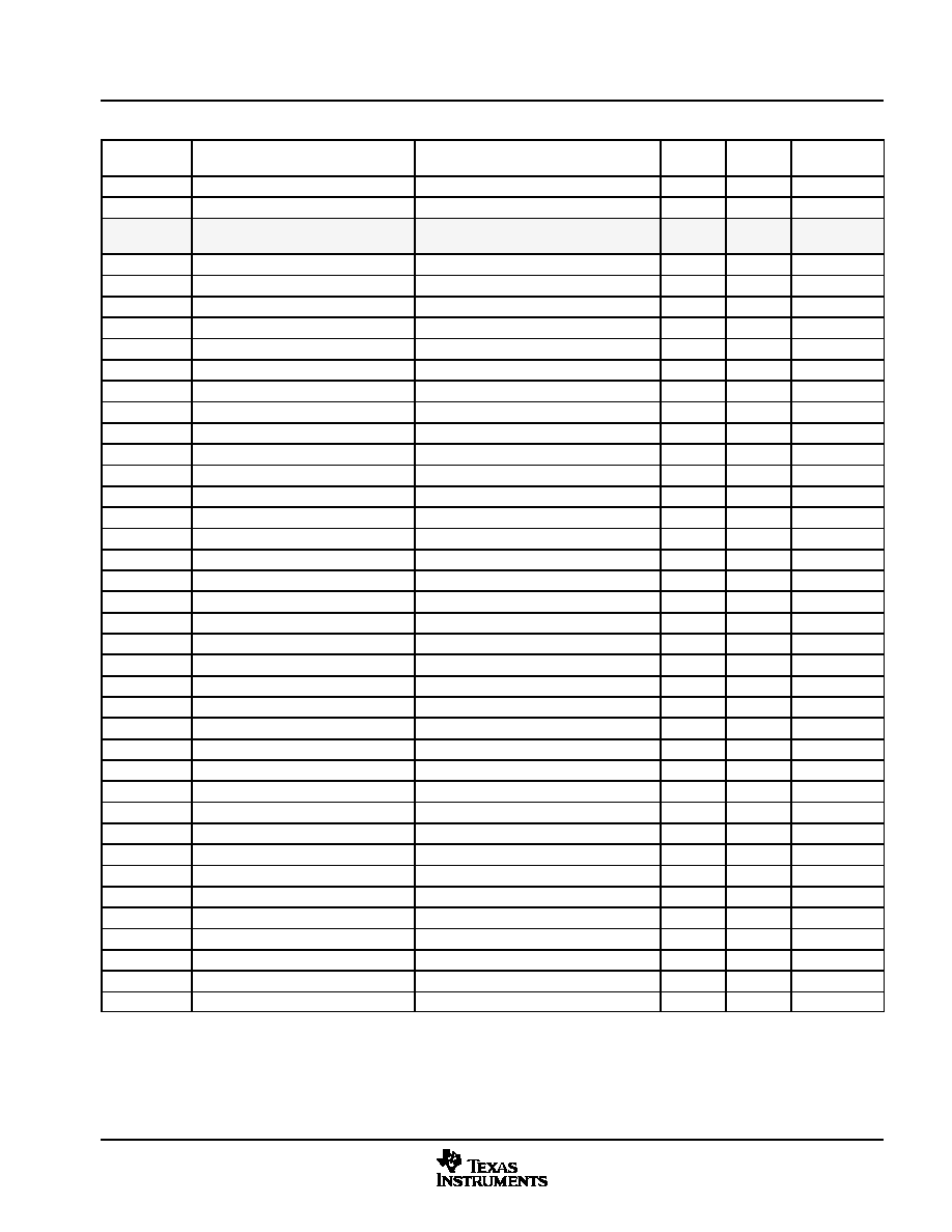
Functional Overview
73
August 2002 - Revised August 2004
SPRS197D
Table 3-18. MPU Level 1 Interrupt Handler Registers
BYTE
ADDRESS
REGISTER NAME
DESCRIPTION
ACCESS
WIDTH
ACCESS
TYPE
RESET
VALUE
FFFE:CB00
MPU_L1_ITR
Interrupt Register
32
RW
0000 0000h
FFFE:CB04
MPU_L1_MIR
Mask Interrupt Register
32
RW
FFFF FFFFh
FFFE:CB08 -
FFFE:CB0C
Reserved
FFFE:CB10
MPU_L1_SIR_IRQ_CODE
IRQ Interrupt Encoded Source Register
32
R
0000 0000h
FFFE:CB14
MPU_L1_SIR_FIQ_CODE
FIQ Interrupt Encoded Source Register
32
R
0000 0000h
FFFE:CB18
MPU_L1_CONTROL_REG
Interrupt Control Register
32
RW
0000 0000h
FFFE:CB1C
MPU_L1_ILR0
Interrupt 0 Priority Level Register
32
RW
0000 0000h
FFFE:CB20
MPU_L1_ILR1
Interrupt 1 Priority Level Register
32
RW
0000 0000h
FFFE:CB24
MPU_L1_ILR2
Interrupt 2 Priority Level Register
32
RW
0000 0000h
FFFE:CB28
MPU_L1_ILR3
Interrupt 3 Priority Level Register
32
RW
0000 0000h
FFFE:CB2C
MPU_L1_ILR4
Interrupt 4 Priority Level Register
32
RW
0000 0000h
FFFE:CB30
MPU_L1_ILR5
Interrupt 5 Priority Level Register
32
RW
0000 0000h
FFFE:CB34
MPU_L1_ILR6
Interrupt 6 Priority Level Register
32
RW
0000 0000h
FFFE:CB38
MPU_L1_ILR7
Interrupt 7 Priority Level Register
32
RW
0000 0000h
FFFE:CB3C
MPU_L1_ILR8
Interrupt 8 Priority Level Register
32
RW
0000 0000h
FFFE:CB40
MPU_L1_ILR9
Interrupt 9 Priority Level Register
32
RW
0000 0000h
FFFE:CB44
MPU_L1_ILR10
Interrupt 10 Priority Level Register
32
RW
0000 0000h
FFFE:CB48
MPU_L1_ILR11
Interrupt 11 Priority Level Register
32
RW
0000 0000h
FFFE:CB4C
MPU_L1_ILR12
Interrupt 12 Priority Level Register
32
RW
0000 0000h
FFFE:CB50
MPU_L1_ILR13
Interrupt 13 Priority Level Register
32
RW
0000 0000h
FFFE:CB54
MPU_L1_ILR14
Interrupt 14 Priority Level Register
32
RW
0000 0000h
FFFE:CB58
MPU_L1_ILR15
Interrupt 15 Priority Level Register
32
RW
0000 0000h
FFFE:CB5C
MPU_L1_ILR16
Interrupt 16 Priority Level Register
32
RW
0000 0000h
FFFE:CB60
MPU_L1_ILR17
Interrupt 17 Priority Level Register
32
RW
0000 0000h
FFFE:CB64
MPU_L1_ILR18
Interrupt 18 Priority Level Register
32
RW
0000 0000h
FFFE:CB68
MPU_L1_ILR19
Interrupt 19 Priority Level Register
32
RW
0000 0000h
FFFE:CB6C
MPU_L1_ILR20
Interrupt 20 Priority Level Register
32
RW
0000 0000h
FFFE:CB70
MPU_L1_ILR21
Interrupt 21 Priority Level Register
32
RW
0000 0000h
FFFE:CB74
MPU_L1_ILR22
Interrupt 22 Priority Level Register
32
RW
0000 0000h
FFFE:CB78
MPU_L1_ILR23
Interrupt 23 Priority Level Register
32
RW
0000 0000h
FFFE:CB7C
MPU_L1_ILR24
Interrupt 24 Priority Level Register
32
RW
0000 0000h
FFFE:CB80
MPU_L1_ILR25
Interrupt 25 Priority Level Register
32
RW
0000 0000h
FFFE:CB84
MPU_L1_ILR26
Interrupt 26 Priority Level Register
32
RW
0000 0000h
FFFE:CB88
MPU_L1_ILR27
Interrupt 27 Priority Level Register
32
RW
0000 0000h
FFFE:CB8C
MPU_L1_ILR28
Interrupt 28 Priority Level Register
32
RW
0000 0000h
FFFE:CB90
MPU_L1_ILR29
Interrupt 29 Priority Level Register
32
RW
0000 0000h
FFFE:CB94
MPU_L1_ILR30
Interrupt 30 Priority Level Register
32
RW
0000 0000h
FFFE:CB98
MPU_L1_ILR31
Interrupt 31 Priority Level Register
32
RW
0000 0000h
FFFE:CB9C
MPU_L1_ISR
Software Interrupt Set Register
32
RW
0000 0000h

Functional Overview
74
August 2002 - Revised August 2004
SPRS197D
Table 3-19. MPU Level 2 Interrupt Handler Registers
BYTE
ADDRESS
REGISTER NAME
DESCRIPTION
ACCESS
WIDTH
ACCESS
TYPE
RESET
VALUE
FFFE:0000
MPU_L2_ITR
Interrupt Register
32
RW
0000 0000h
FFFE:0004
MPU_L2_MIR
Mask Interrupt Register
32
RW
FFFF FFFFh
FFFE:0008 -
FFFE:000C
Reserved
FFFE:0010
MPU_L2_SIR_IRQ_CODE
IRQ Interrupt Encoded Source Register
32
R
0000 0000h
FFFE:0014
MPU_L2_SIR_FIQ_CODE
FIQ Interrupt Encoded Source Register
32
R
0000 0000h
FFFE:0018
MPU_L2_CONTROL_REG
Interrupt Control Register
32
RW
0000 0000h
FFFE:001C
MPU_L2_ILR0
Interrupt 0 Priority Level Register
32
RW
0000 0000h
FFFE:0020
MPU_L2_ILR1
Interrupt 1 Priority Level Register
32
RW
0000 0000h
FFFE:0024
MPU_L2_ILR2
Interrupt 2 Priority Level Register
32
RW
0000 0000h
FFFE:0028
MPU_L2_ILR3
Interrupt 3 Priority Level Register
32
RW
0000 0000h
FFFE:002C
MPU_L2_ILR4
Interrupt 4 Priority Level Register
32
RW
0000 0000h
FFFE:0030
MPU_L2_ILR5
Interrupt 5 Priority Level Register
32
RW
0000 0000h
FFFE:0034
MPU_L2_ILR6
Interrupt 6 Priority Level Register
32
RW
0000 0000h
FFFE:0038
MPU_L2_ILR7
Interrupt 7 Priority Level Register
32
RW
0000 0000h
FFFE:003C
MPU_L2_ILR8
Interrupt 8 Priority Level Register
32
RW
0000 0000h
FFFE:0040
MPU_L2_ILR9
Interrupt 9 Priority Level Register
32
RW
0000 0000h
FFFE:0044
MPU_L2_ILR10
Interrupt 10 Priority Level Register
32
RW
0000 0000h
FFFE:0048
MPU_L2_ILR11
Interrupt 11 Priority Level Register
32
RW
0000 0000h
FFFE:004C
MPU_L2_ILR12
Interrupt 12 Priority Level Register
32
RW
0000 0000h
FFFE:0050
MPU_L2_ILR13
Interrupt 13 Priority Level Register
32
RW
0000 0000h
FFFE:0054
MPU_L2_ILR14
Interrupt 14 Priority Level Register
32
RW
0000 0000h
FFFE:0058
MPU_L2_ILR15
Interrupt 15 Priority Level Register
32
RW
0000 0000h
FFFE:005C
MPU_L2_ILR16
Interrupt 16 Priority Level Register
32
RW
0000 0000h
FFFE:0060
MPU_L2_ILR17
Interrupt 17 Priority Level Register
32
RW
0000 0000h
FFFE:0064
MPU_L2_ILR18
Interrupt 18 Priority Level Register
32
RW
0000 0000h
FFFE:0068
MPU_L2_ILR19
Interrupt 19 Priority Level Register
32
RW
0000 0000h
FFFE:006C
MPU_L2_ILR20
Interrupt 20 Priority Level Register
32
RW
0000 0000h
FFFE:0070
MPU_L2_ILR21
Interrupt 21 Priority Level Register
32
RW
0000 0000h
FFFE:0074
MPU_L2_ILR22
Interrupt 22 Priority Level Register
32
RW
0000 0000h
FFFE:0078
MPU_L2_ILR23
Interrupt 23 Priority Level Register
32
RW
0000 0000h
FFFE:007C
MPU_L2_ILR24
Interrupt 24 Priority Level Register
32
RW
0000 0000h
FFFE:0080
MPU_L2_ILR25
Interrupt 25 Priority Level Register
32
RW
0000 0000h
FFFE:0084
MPU_L2_ILR26
Interrupt 26 Priority Level Register
32
RW
0000 0000h
FFFE:0088
MPU_L2_ILR27
Interrupt 27 Priority Level Register
32
RW
0000 0000h
FFFE:008C
MPU_L2_ILR28
Interrupt 28 Priority Level Register
32
RW
0000 0000h
FFFE:0090
MPU_L2_ILR29
Interrupt 29 Priority Level Register
32
RW
0000 0000h
FFFE:0094
MPU_L2_ILR30
Interrupt 30 Priority Level Register
32
RW
0000 0000h
FFFE:0098
MPU_L2_ILR31
Interrupt 31 Priority Level Register
32
RW
0000 0000h
FFFE:009C
MPU_L2_ISR
Software Interrupt Set Register
32
RW
0000 0000h

Functional Overview
75
August 2002 - Revised August 2004
SPRS197D
Table 3-20. System DMA Controller Registers
BYTE
ADDRESS
REGISTER NAME
DESCRIPTION
ACCESS
WIDTH
ACCESS
TYPE
RESET
VALUE
FFFE:D800
SYS_DMA_CSDP_CH0
Channel 0 Source/Destination Parameters Register
16
RW
0000h
FFFE:D802
SYS_DMA_CCR_CH0
Channel 0 Control Register
16
RW
0000h
FFFE:D804
SYS_DMA_CICR_CH0
Channel 0 Interrupt Control Register
16
RW
0003h
FFFE:D806
SYS_DMA_CSR_CH0
Channel 0 Status Register
16
R
0000h
FFFE:D808
SYS_DMA_CSSA_L_CH0
Channel 0 Source Start Address Register LSB
16
RW
undef
FFFE:D80A
SYS_DMA_CSSA_U_CH0
Channel 0 Source Start Address Register MSB
16
RW
undef
FFFE:D80C
SYS_DMA_CDSA_L_CH0
Channel 0 Destination Start Address Register LSB
16
RW
undef
FFFE:D80E
SYS_DMA_CDSA_U_CH0
Channel 0 Destination Start Address Register MSB
16
RW
undef
FFFE:D810
SYS_DMA_CEN_CH0
Channel 0 Element Number Register
16
RW
undef
FFFE:D812
SYS_DMA_CFN_CH0
Channel 0 Frame Number Register
16
RW
undef
FFFE:D814
SYS_DMA_CFI_CH0
Channel 0 Frame Index Register
16
RW
undef
FFFE:D816
SYS_DMA_CEI_CH0
Channel 0 Element Index Register
16
RW
undef
FFFE:D818
SYS_DMA_CPC_CH0
Channel 0 Progress Counter Register
16
RW
undef
FFFE:D81A -
FFFE:083E
Reserved
FFFE:D840
SYS_DMA_CSDP_CH1
Channel 1 Source/Destination Parameters Register
16
RW
0000h
FFFE:D842
SYS_DMA_CCR_CH1
Channel 1 Control Register
16
RW
0000h
FFFE:D844
SYS_DMA_CICR_CH1
Channel 1 Interrupt Control Register
16
RW
0003h
FFFE:D846
SYS_DMA_CSR_CH1
Channel 1 Status Register
16
R
0000h
FFFE:D848
SYS_DMA_CSSA_L_CH1
Channel 1 Source Start Address Register LSB
16
RW
undef
FFFE:D84A
SYS_DMA_CSSA_U_CH1
Channel 1 Source Start Address Register MSB
16
RW
undef
FFFE:D84C
SYS_DMA_CDSA_L_CH1
Channel 1 Destination Start Address Register LSB
16
RW
undef
FFFE:D84E
SYS_DMA_CDSA_U_CH1
Channel 1 Destination Start Address Register MSB
16
RW
undef
FFFE:D850
SYS_DMA_CEN_CH1
Channel 1 Element Number Register
16
RW
undef
FFFE:D852
SYS_DMA_CFN_CH1
Channel 1 Frame Number Register
16
RW
undef
FFFE:D854
SYS_DMA_CFI_CH1
Channel 1 Frame Index Register
16
RW
undef
FFFE:D856
SYS_DMA_CEI_CH1
Channel 1 Element Index Register
16
RW
undef
FFFE:D858
SYS_DMA_CPC_CH1
Channel 1 Progress Counter Register
16
RW
undef
FFFE:D85A -
FFFE:D87E
Reserved
FFFE:D880
SYS_DMA_CSDP_CH2
Channel 2 Source/Destination Parameters Register
16
RW
0000h
FFFE:D882
SYS_DMA_CCR_CH2
Channel 2 Control Register
16
RW
0000h
FFFE:D884
SYS_DMA_CICR_CH2
Channel 2 Interrupt Control Register
16
RW
0003h
FFFE:D886
SYS_DMA_CSR_CH2
Channel 2 Status Register
16
R
0000h
FFFE:D888
SYS_DMA_CSSA_L_CH2
Channel 2 Source Start Address Register LSB
16
RW
undef
FFFE:D88A
SYS_DMA_CSSA_U_CH2
Channel 2 Source Start Address Register MSB
16
RW
undef
FFFE:D88C
SYS_DMA_CDSA_L_CH2
Channel 2 Destination Start Address Register LSB
16
RW
undef
FFFE:D88E
SYS_DMA_CDSA_U_CH2
Channel 2 Destination Start Address Register MSB
16
RW
undef
FFFE:D890
SYS_DMA_CEN_CH2
Channel 2 Element Number Register
16
RW
undef
FFFE:D892
SYS_DMA_CFN_CH2
Channel 2 Frame Number Register
16
RW
undef
FFFE:D894
SYS_DMA_CFI_CH2
Channel 2 Frame Index Register
16
RW
undef
FFFE:D896
SYS_DMA_CEI_CH2
Channel 2 Element Index Register
16
RW
undef
FFFE:D898
SYS_DMA_CPC_CH2
Channel 2 Progress Counter Register
16
RW
undef

Functional Overview
76
August 2002 - Revised August 2004
SPRS197D
Table 3-20. System DMA Controller Registers (Continued)
RESET
VALUE
ACCESS
TYPE
ACCESS
WIDTH
DESCRIPTION
REGISTER NAME
BYTE
ADDRESS
FFFE:D89A -
FFFE:D8BE
Reserved
FFFE:D8C0
SYS_DMA_CSDP_CH3
Channel 3 Source/Destination Parameters Register
16
RW
0000h
FFFE:D8C2
SYS_DMA_CCR_CH3
Channel 3 Control Register
16
RW
0000h
FFFE:D8C4
SYS_DMA_CICR_CH3
Channel 3 Interrupt Control Register
16
RW
0003h
FFFE:D8C6
SYS_DMA_CSR_CH3
Channel 3 Status Register
16
R
0000h
FFFE:D8C8
SYS_DMA_CSSA_L_CH3
Channel 3 Source Start Address Register LSB
16
RW
undef
FFFE:D8CA
SYS_DMA_CSSA_U_CH3
Channel 3 Source Start Address Register MSB
16
RW
undef
FFFE:D8CC
SYS_DMA_CDSA_L_CH3
Channel 3 Destination Start Address Register LSB
16
RW
undef
FFFE:D8CE
SYS_DMA_CDSA_U_CH3
Channel 3 Destination Start Address Register MSB
16
RW
undef
FFFE:D8D0
SYS_DMA_CEN_CH3
Channel 3 Element Number Register
16
RW
undef
FFFE:D8D2
SYS_DMA_CFN_CH3
Channel 3 Frame Number Register
16
RW
undef
FFFE:D8D4
SYS_DMA_CFI_CH3
Channel 3 Frame Index Register
16
RW
undef
FFFE:D8D6
SYS_DMA_CEI_CH3
Channel 3 Element Index Register
16
RW
undef
FFFE:D8D8
SYS_DMA_CPC_CH3
Channel 3 Progress Counter Register
16
RW
undef
FFFE:D8DA -
FFFE:D8FE
Reserved
FFFE:D900
SYS_DMA_CSDP_CH4
Channel 4 Source/Destination Parameters Register
16
RW
0000h
FFFE:D902
SYS_DMA_CCR_CH4
Channel 4 Control Register
16
RW
0000h
FFFE:D904
SYS_DMA_CICR_CH4
Channel 4 Interrupt Control Register
16
RW
0003h
FFFE:D906
SYS_DMA_CSR_CH4
Channel 4 Status Register
16
R
0000h
FFFE:D908
SYS_DMA_CSSA_L_CH4
Channel 4 Source Start Address Register LSB
16
RW
undef
FFFE:D90A
SYS_DMA_CSSA_U_CH4
Channel 4 Source Start Address Register MSB
16
RW
undef
FFFE:D90C
SYS_DMA_CDSA_L_CH4
Channel 4 Destination Start Address Register LSB
16
RW
undef
FFFE:D90E
SYS_DMA_CDSA_U_CH4
Channel 4 Destination Start Address Register MSB
16
RW
undef
FFFE:D910
SYS_DMA_CEN_CH4
Channel 4 Element Number Register
16
RW
undef
FFFE:D912
SYS_DMA_CFN_CH4
Channel 4 Frame Number Register
16
RW
undef
FFFE:D914
SYS_DMA_CFI_CH4
Channel 4 Frame Index Register
16
RW
undef
FFFE:D916
SYS_DMA_CEI_CH4
Channel 4 Element Index Register
16
RW
undef
FFFE:D918
SYS_DMA_CPC_CH4
Channel 4 Progress Counter Register
16
RW
undef
FFFE:D91A -
FFFE:D93E
Reserved
FFFE:D940
SYS_DMA_CSDP_CH5
Channel 5 Source/Destination Parameters Register
16
RW
0000h
FFFE:D942
SYS_DMA_CCR_CH5
Channel 5 Control Register
16
RW
0000h
FFFE:D944
SYS_DMA_CICR_CH5
Channel 5 Interrupt Control Register
16
RW
0003h
FFFE:D946
SYS_DMA_CSR_CH5
Channel 5 Status Register
16
R
0000h
FFFE:D948
SYS_DMA_CSSA_L_CH5
Channel 5 Source Start Address Register LSB
16
RW
undef
FFFE:D94A
SYS_DMA_CSSA_U_CH5
Channel 5 Source Start Address Register MSB
16
RW
undef
FFFE:D94C
SYS_DMA_CDSA_L_CH5
Channel 5 Destination Start Address Register LSB
16
RW
undef
FFFE:D94E
SYS_DMA_CDSA_U_CH5
Channel 5 Destination Start Address Register MSB
16
RW
undef
FFFE:D950
SYS_DMA_CEN_CH5
Channel 5 Element Number Register
16
RW
undef
FFFE:D952
SYS_DMA_CFN_CH5
Channel 5 Frame Number Register
16
RW
undef
FFFE:D954
SYS_DMA_CFI_CH5
Channel 5 Frame Index Register
16
RW
undef
FFFE:D956
SYS_DMA_CEI_CH5
Channel 5 Element Index Register
16
RW
undef

Functional Overview
77
August 2002 - Revised August 2004
SPRS197D
Table 3-20. System DMA Controller Registers (Continued)
RESET
VALUE
ACCESS
TYPE
ACCESS
WIDTH
DESCRIPTION
REGISTER NAME
BYTE
ADDRESS
FFFE:D958
SYS_DMA_CPC_CH5
Channel 5 Progress Counter Register
16
RW
undef
FFFE:D95A -
FFFE:D97E
Reserved
FFFE:D980
SYS_DMA_CSDP_CH6
Channel 6 Source/Destination Parameters Register
16
RW
0000h
FFFE:D982
SYS_DMA_CCR_CH6
Channel 6 Control Register
16
RW
0000h
FFFE:D984
SYS_DMA_CICR_CH6
Channel 6 Interrupt Control Register
16
RW
0003h
FFFE:D986
SYS_DMA_CSR_CH6
Channel 6 Status Register
16
R
0000h
FFFE:D988
SYS_DMA_CSSA_L_CH6
Channel 6 Source Start Address Register LSB
16
RW
undef
FFFE:D98A
SYS_DMA_CSSA_U_CH6
Channel 6 Source Start Address Register MSB
16
RW
undef
FFFE:D98C
SYS_DMA_CDSA_L_CH6
Channel 6 Destination Start Address Register LSB
16
RW
undef
FFFE:D98E
SYS_DMA_CDSA_U_CH6
Channel 6 Destination Start Address Register MSB
16
RW
undef
FFFE:D990
SYS_DMA_CEN_CH6
Channel 6 Element Number Register
16
RW
undef
FFFE:D992
SYS_DMA_CFN_CH6
Channel 6 Frame Number Register
16
RW
undef
FFFE:D994
SYS_DMA_CFI_CH6
Channel 6 Frame Index Register
16
RW
undef
FFFE:D996
SYS_DMA_CEI_CH6
Channel 6 Element Index Register
16
RW
undef
FFFE:D998
SYS_DMA_CPC_CH6
Channel 6 Progress Counter Register
16
RW
undef
FFFE:D99A -
FFFE:D9BE
Reserved
FFFE:D9C0
SYS_DMA_CSDP_CH7
Channel 7 Source/Destination Parameters Register
16
RW
0000h
FFFE:D9C2
SYS_DMA_CCR_CH7
Channel 7 Control Register
16
RW
0000h
FFFE:D9C4
SYS_DMA_CICR_CH7
Channel 7 Interrupt Control Register
16
RW
0003h
FFFE:D9C6
SYS_DMA_CSR_CH7
Channel 7 Status Register
16
R
0000h
FFFE:D9C8
SYS_DMA_CSSA_L_CH7
Channel 7 Source Start Address Register LSB
16
RW
undef
FFFE:D9CA
SYS_DMA_CSSA_U_CH7
Channel 7 Source Start Address Register MSB
16
RW
undef
FFFE:D9CC
SYS_DMA_CDSA_L_CH7
Channel 7 Destination Start Address Register LSB
16
RW
undef
FFFE:D9CE
SYS_DMA_CDSA_U_CH7
Channel 7 Destination Start Address Register MSB
16
RW
undef
FFFE:D9D0
SYS_DMA_CEN_CH7
Channel 7 Element Number Register
16
RW
undef
FFFE:D9D2
SYS_DMA_CFN_CH7
Channel 7 Frame Number Register
16
RW
undef
FFFE:D9D4
SYS_DMA_CFI_CH7
Channel 7 Frame Index Register
16
RW
undef
FFFE:D9D6
SYS_DMA_CEI_CH7
Channel 7 Element Index Register
16
RW
undef
FFFE:D9D8
SYS_DMA_CPC_CH7
Channel 7 Progress Counter Register
16
RW
undef
FFFE:D9DA -
FFFE:D9FE
Reserved
FFFE:DA00
SYS_DMA_CSDP_CH8
Channel 8 Source/Destination Parameters Register
16
RW
0000h
FFFE:DA02
SYS_DMA_CCR_CH8
Channel 8 Control Register
16
RW
0000h
FFFE:DA04
SYS_DMA_CICR_CH8
Channel 8 Interrupt Control Register
16
RW
0003h
FFFE:DA06
SYS_DMA_CSR_CH8
Channel 8 Status Register
16
R
0000h
FFFE:DA08
SYS_DMA_CSSA_L_CH8
Channel 8 Source Start Address Register LSB
16
RW
undef
FFFE:DA0A
SYS_DMA_CSSA_U_CH8
Channel 8 Source Start Address Register MSB
16
RW
undef
FFFE:DA0C
SYS_DMA_CDSA_L_CH8
Channel 8 Destination Start Address Register LSB
16
RW
undef
FFFE:DA0E
SYS_DMA_CDSA_U_CH8
Channel 8 Destination Start Address Register MSB
16
RW
undef
FFFE:DA10
SYS_DMA_CEN_CH8
Channel 8 Element Number Register
16
RW
undef
FFFE:DA12
SYS_DMA_CFN_CH8
Channel 8 Frame Number Register
16
RW
undef
FFFE:DA14
SYS_DMA_CFI_CH8
Channel 8 Frame Index Register
16
RW
undef
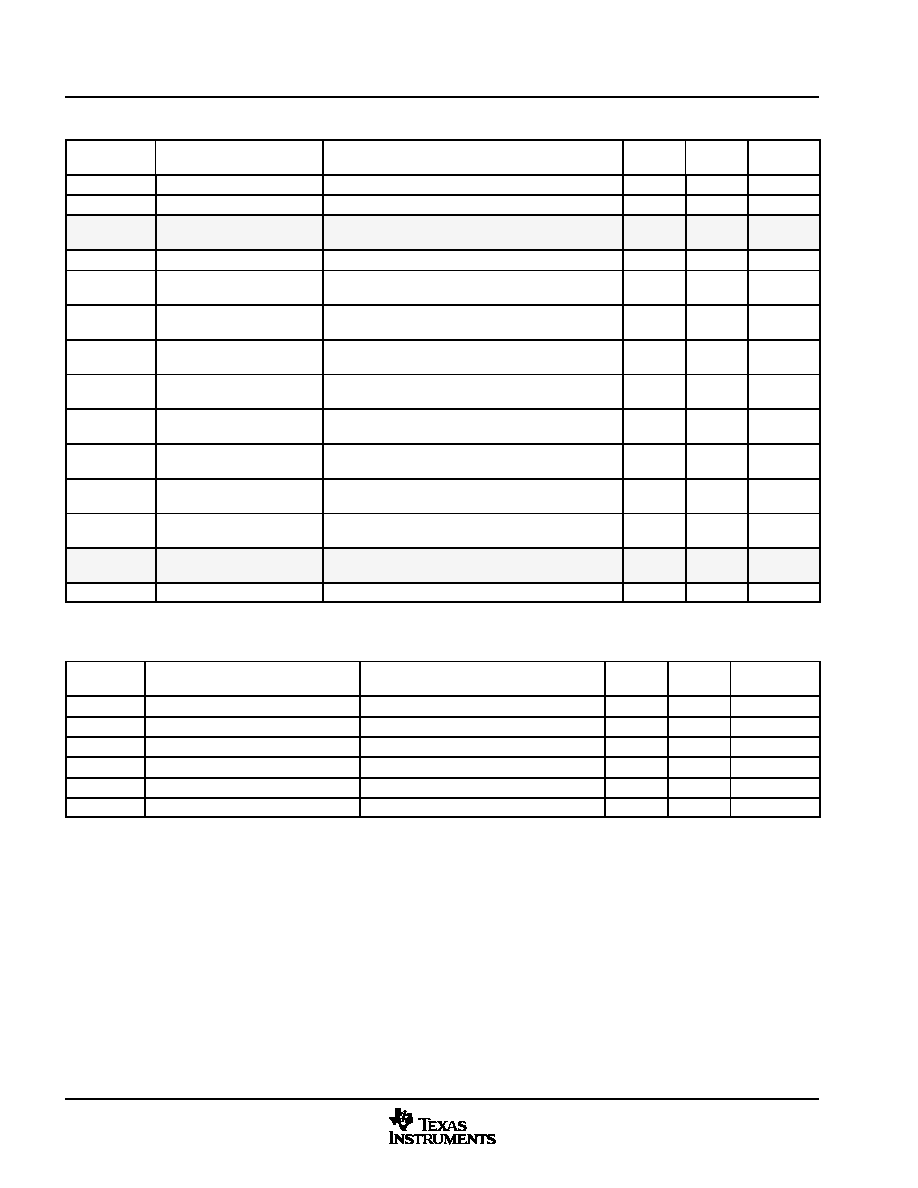
Functional Overview
78
August 2002 - Revised August 2004
SPRS197D
Table 3-20. System DMA Controller Registers (Continued)
RESET
VALUE
ACCESS
TYPE
ACCESS
WIDTH
DESCRIPTION
REGISTER NAME
BYTE
ADDRESS
FFFE:DA16
SYS_DMA_CEI_CH8
Channel 8 Element Index Register
16
RW
undef
FFFE:DA18
SYS_DMA_CPC_CH8
Channel 8 Progress Counter Register
16
RW
undef
FFFE:DA1A -
FFFE:DAFE
Reserved
FFFE:DB00
SYS_DMA_LCD_CTRL
LCD Channel Control Register
16
RW
0000h
FFFE:DB02
SYS_DMA_LCD_TOP_F1_L LCD Channel Top Address Frame Buffer 1 Register
LSB
16
RW
undef
FFFE:DB04
SYS_DMA_LCD_TOP_F1_U LCD Channel Top Address Frame Buffer 1 Register
MSB
16
RW
undef
FFFE:DB06
SYS_DMA_LCD_BOT_F1_L LCD Channel Bottom Address Frame Buffer 1
Register LSB
16
RW
undef
FFFE:DB08
SYS_DMA_LCD_BOT_F1_U LCD Channel Bottom Address Frame Buffer 1
Register MSB
16
RW
undef
FFFE:DB0A
SYS_DMA_LCD_TOP_F2_L LCD Channel Top Address Frame Buffer 2 Register
LSB
16
RW
undef
FFFE:DB0C
SYS_DMA_LCD_TOP_F2_U LCD Channel Top Address Frame Buffer 2 Register
MSB
16
RW
undef
FFFE:DB0E
SYS_DMA_LCD_BOT_F2_L LCD Channel Bottom Address Frame Buffer 2
Register LSB
16
RW
undef
FFFE:DB10
SYS_DMA_LCD_BOT_F2_U LCD Channel Bottom Address Frame Buffer 2
Register MSB
16
RW
undef
FFFE:DB12 -
FFFE:DBFE
Reserved
FFFE:DC00
SYS_DMA_GCR
DMA Global Control Register
16
RW
0008h
Table 3-21. LCD Controller Registers
BYTE
ADDRESS
REGISTER NAME
DESCRIPTION
ACCESS
WIDTH
ACCESS
TYPE
RESET
VALUE
FFFE:C000
LCD_CONTROL
LCD Control Register
32
RW
0x0000 0000
FFFE:C004
LCD_TIMING0
LCD Timing 0 Register
32
RW
undef
FFFE:C008
LCD_TIMING1
LCD Timing 1 Register
32
RW
0x0000 0000
FFFE:C00C
LCD_TIMING2
LCD Timing 2 Register
32
RW
0x0000 0000
FFFE:C010
LCD_STATUS
LCD Status Register
32
RW
0x0000 0000
FFFE:C014
LCD_SUBPANEL
LCD Subpanel Display Register
32
RW
0x0000 0000

Functional Overview
79
August 2002 - Revised August 2004
SPRS197D
3.15.2
MPU Public Peripheral Registers
The MPU public peripheral registers include the following:
�
Serial Ports
-
McBSP2 Registers
-
MICROWIRE Registers
-
I
2
C Registers
-
HDQ/1-Wire Interface Registers
-
MMC/SD Registers
-
USB Function Registers
-
USB Host Registers
�
Parallel Ports
-
Camera Interface Registers
�
Human Interface support
-
MPUIO/Keyboard Registers
-
PWL Registers
-
PWT Registers
-
LED Pulse Generator 1 Registers
-
LED Pulse Generator 2 Registers
�
Timers and Counters
-
32k Timer Registers
-
Real-Time Clock Registers
-
Frame Adjustment Counter Registers

Functional Overview
80
August 2002 - Revised August 2004
SPRS197D
Table 3-22. McBSP2 Registers
BYTE
ADDRESS
REGISTER NAME
DESCRIPTION
ACCESS
WIDTH
ACCESS
TYPE
RESET
VALUE
FFFB:1000
MCBSP2_DRR2
McBSP2 Data Receive Register 2
16
RW
0000h
FFFB:1002
MCBSP2_DRR1
McBSP2 Data Receive Register 1
16
RW
0000h
FFFB:1004
MCBSP2_DXR2
McBSP2 Data Transmit Register 2
16
RW
0000h
FFFB:1006
MCBSP2_DXR1
McBSP2 Data Transmit Register 1
16
RW
0000h
FFFB:1008
MCBSP2_SPCR2
McBSP2 Serial Port Control Register 2
16
RW
0000h
FFFB:100A
MCBSP2_SPCR1
McBSP2 Serial Port Control Register 1
16
RW
0000h
FFFB:100C
MCBSP2_RCR2
McBSP2 Receive Control Register 2
16
RW
0000h
FFFB:100E
MCBSP2_RCR1
McBSP2 Receive Control Register 1
16
RW
0000h
FFFB:1010
MCBSP2_XCR2
McBSP2 Transmit Control Register 2
16
RW
0000h
FFFB:1012
MCBSP2_XCR1
McBSP2 Transmit Control Register 1
16
RW
0000h
FFFB:1014
MCBSP2_SRGR2
McBSP2 Sample Rate Generator Register 2
16
RW
2000h
FFFB:1016
MCBSP2_SRGR1
McBSP2 Sample Rate Generator Register 1
16
RW
0001h
FFFB:1018
MCBSP2_MCR2
McBSP2 Multichannel Control Register 2
16
RW
0000h
FFFB:101A
MCBSP2_MCR1
McBSP2 Multichannel Control Register 1
16
RW
0000h
FFFB:101C
MCBSP2_RCERA
McBSP2 Receive Channel Enable Register Partition A
16
RW
0000h
FFFB:101E
MCBSP2_RCERB
McBSP2 Receive Channel Enable Register Partition B
16
RW
0000h
FFFB:1020
MCBSP2_XCERA
McBSP2 Transmit Channel Enable Register Partition A
16
RW
0000h
FFFB:1022
MCBSP2_XCERB
McBSP2 Transmit Channel Enable Register Partition B
16
RW
0000h
FFFB:1024
MCBSP2_PCR0
McBSP2 Pin Control Register 0
16
RW
0000h
FFFB:1026
MCBSP2_RCERC
McBSP2 Receive Channel Enable Register Partition C
16
RW
0000h
FFFB:1028
MCBSP2_RCERD
McBSP2 Receive Channel Enable Register Partition D
16
RW
0000h
FFFB:102A
MCBSP2_XCERC
McBSP2 Transmit Channel Enable Register Partition C
16
RW
0000h
FFFB:102C
MCBSP2_XCERD
McBSP2 Transmit Channel Enable Register Partition D
16
RW
0000h
FFFB:102E
MCBSP2_RCERE
McBSP2 Receive Channel Enable Register Partition E
16
RW
0000h
FFFB:1030
MCBSP2_RCERF
McBSP2 Receive Channel Enable Register Partition F
16
RW
0000h
FFFB:1032
MCBSP2_XCERE
McBSP2 Transmit Channel Enable Register Partition E
16
RW
0000h
FFFB:1034
MCBSP2_XCERF
McBSP2 Transmit Channel Enable Register Partition F
16
RW
0000h
FFFB:1036
MCBSP2_RCERG
McBSP2 Receive Channel Enable Register Partition G
16
RW
0000h
FFFB:1038
MCBSP2_RCERH
McBSP2 Receive Channel Enable Register Partition H
16
RW
0000h
FFFB:103A
MCBSP2_XCERG
McBSP2 Transmit Channel Enable Register Partition G
16
RW
0000h
FFFB:103C
MCBSP2_XCERH
McBSP2 Transmit Channel Enable Register Partition H
16
RW
0000h
Table 3-23. MICROWIRE Registers
BYTE
ADDRESS
REGISTER NAME
DESCRIPTION
ACCESS
WIDTH
ACCESS
TYPE
RESET
VALUE
FFFB:3000
TD
MICROWIRE Transmit Data Register
16
W
undef
FFFB:3000
RD
MICROWIRE Receive Data Register
16
R
undef
FFFB:3004
CSR
MICROWIRE Control and Status Register
16
RW
undef
FFFB:3008
SR1
MICROWIRE Setup Register 1
16
RW
undef
FFFB:300C
SR2
MICROWIRE Setup Register 2
16
RW
undef
FFFB:3010
SR3
MICROWIRE Setup Register 3
16
RW
0000h
FFFB:3014
SR4
MICROWIRE Setup Register 4
16
RW
0000h
FFFB:3018
SR5
MICROWIRE Setup Register 5
16
RW
0000h

Functional Overview
81
August 2002 - Revised August 2004
SPRS197D
Table 3-24. I
2
C Registers
BYTE
ADDRESS
REGISTER NAME
DESCRIPTION
ACCESS
WIDTH
ACCESS
TYPE
RESET
VALUE
FFFB:3800
I2C_REV
I
2
C Module Version Register
16
RW
0011h
FFFB:3804
I2C_IE
I
2
C Interrupt Enable Register
16
RW
0000h
FFFB:3808
I2C_STAT
I
2
C Status Register
16
R
0000h
FFFB:380C
I2C_IV
I
2
C Interrupt Vector Register
16
R
0000h
FFFB:3810
Reserved
FFFB:3814
I2C_BUF
I
2
C Buffer Configuration Register
16
RW
0000h
FFFB:3818
I2C_CNT
I
2
C Data Counter Register
16
RW
0000h
FFFB:381C
I2C_DATA
I
2
C Data Access Register
16
RW
0000h
FFFB:3820
Reserved
FFFB:3824
I2C_CON
I
2
C Configuration Register
16
RW
0000h
FFFB:3828
I2C_OA
I
2
C Own Address Register
16
RW
0000h
FFFB:382C
I2C_SA
I
2
C Slave Address Register
16
RW
03FFh
FFFB:3830
I2C_PSC
I
2
C Clock Prescaler Register
16
RW
0000h
FFFB:3834
I2C_SCLL
I
2
C SCL Low Timer Register
16
RW
0000h
FFFB:3838
I2C_SCLH
I
2
C SCL High Timer Register
16
RW
0000h
FFFB:383C
I2C_SYSTEST
I
2
C System Test Register
16
RW
0000h
Table 3-25. HDQ/1-Wire Interface Registers
BYTE
ADDRESS
REGISTER NAME
DESCRIPTION
ACCESS
WIDTH
ACCESS
TYPE
RESET
VALUE
FFFB:C000
TXR
TX Write Data Register
8
RW
00h
FFFB:C004
RXR
RX Receive Buffer Register
8
R
undef
FFFB:C008
CSR
Control and Status Register
8
RW
00h
FFFB:C00C
ISR
Interrupt Status Register
8
RW
00h
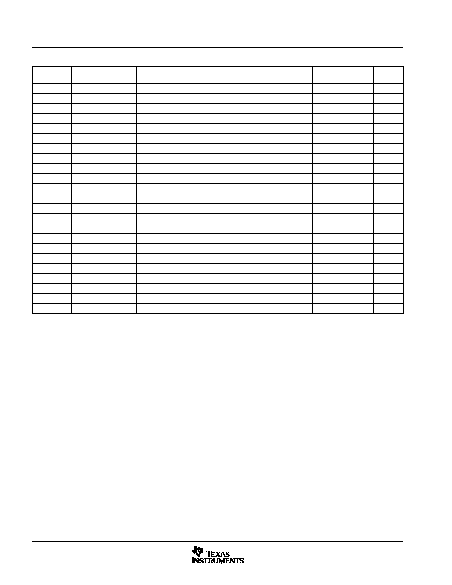
Functional Overview
82
August 2002 - Revised August 2004
SPRS197D
Table 3-26. MMC/SD Registers
BYTE
ADDRESS
REGISTER NAME
DESCRIPTION
ACCESS
WIDTH
ACCESS
TYPE
RESET
VALUE
FFFB:7800
MMC_CMD
MMC Command
16
RW
0000h
FFFB:7804
MMC_ARGL
MMC Argument Low
16
RW
0000h
FFFB:7808
MMC_ARGH
MMC Argument High
16
RW
0000h
FFFB:780C
MMC_CON
MMC System Configuration
16
RW
0000h
FFFB:7810
MMC_STAT
MMC Status
16
RW
0000h
FFFB:7814
MMC_IE
MMC System Interrupt Enable
16
RW
0000h
FFFB:7818
MMC_CTO
MMC Command Timeout
16
RW
0000h
FFFB:781C
MMC_DTO
MMC Data Timeout
16
RW
0000h
FFFB:7820
MMC_DATA
MMC TX/RX FIFO Data
16
RW
0000h
FFFB:7824
MMC_BLEN
MMC Block Length
16
RW
0000h
FFFB:7828
MMC_NBLK
MMC Number Of Blocks
16
RW
0000h
FFFB:782C
MMC_BUF
MMC Buffer Configuration
16
RW
1F00h
FFFB:7834
MMC_SDIO
MMC SDIO Mode Configuration
16
RW
0000h
FFFB:7838
MMC_SYST
MMC System Test
16
RW
2000h
FFFB:783C
MMC_REV
MMC Module Version
16
R
-
FFFB:7840
MMC_RSP0
MMC Command Response 0
16
R
undef
FFFB:7844
MMC_RSP1
MMC Command Response 1
16
R
undef
FFFB:7848
MMC_RSP2
MMC Command Response 2
16
R
undef
FFFB:784C
MMC_RSP3
MMC Command Response 3
16
R
undef
FFFB:7850
MMC_RSP4
MMC Command Response 4
16
R
undef
FFFB:7854
MMC_RSP5
MMC Command Response 5
16
R
undef
FFFB:7858
MMC_RSP6
MMC Command Response 6
16
R
undef
FFFB:785C
MMC_RSP7
MMC Command Response 7
16
R
undef

Functional Overview
83
August 2002 - Revised August 2004
SPRS197D
Table 3-27. USB Function Registers
BYTE
ADDRESS
REGISTER NAME
DESCRIPTION
ACCESS
WIDTH
ACCESS
TYPE
RESET
VALUE
FFFB:4000
REV
Revision Register
16
R
-
FFFB:4004
EP_NUM
Endpoint Selection Register
16
RW
0000h
FFFB:4008
DATA
Data Register
16
RW
undef
FFFB:400C
CTRL
Control Register
16
RW
0000h
FFFB:4010
STAT_FLG
Status Flag Register
16
R
0202h
FFFB:4014
RXFSTAT
Receive FIFO Status Register
16
R
0000h
FFFB:4018
SYSCON1
System Configuration 1 Register
16
RW
0000h
FFFB:401C
SYSCON2
System Configuration 2 Register
16
RW
0000h
FFFB:4020
DEVSTAT
Device Status Register
16
R
undef
FFFB:4024
SOF
Start of Frame Register
16
R
0000h
FFFB:4028
IRQ_EN
Interrupt Enable Register
16
RW
undef
FFFB:402C
DMA_IRQ_EN
DMA Interrupt Enable Register
16
RW
undef
FFFB:4030
IRQ_SRC
Interrupt Source Register
16
RW
0000h
FFFB:4034
EPN_STAT
Endpoint Interrupt Status Register
16
R
0000h
FFFB:4038
DMAN_STAT
DMA Endpoint Interrupt Status Register
16
R
0000h
FFFB:403C
Reserved
FFFB:4040
RXDMA_CFG
Receive Channels DMA Configuration Register
16
RW
0000h
FFFB:4044
TXDMA_CFG
Transmit Channels DMA Configuration Register
16
RW
0000h
FFFB:4048
DATA_DMA
DMA FIFO Data Register
16
RW
undef
FFFB:404C
Reserved
FFFB:4050
TXDMA0
Transmit DMA Control 0 Register
16
RW
0000h
FFFB:4054
TXDMA1
Transmit DMA Control 1 Register
16
RW
0000h
FFFB:4058
TXDMA2
Transmit DMA Control 2 Register
16
RW
0000h
FFFB:405C
Reserved
FFFB:4060
RXDMA0
Receive DMA Control 0 Register
16
RW
0000h
FFFB:4064
RXDMA1
Receive DMA Control 1 Register
16
RW
0000h
FFFB:4068
RXDMA2
Receive DMA Control 2 Register
16
RW
0000h
FFFB:406C -
FFFB:407C
Reserved
FFFB:4080
EP0
Endpoint Configuration 0 Register
16
RW
0000h
FFFB:4084
EP1_RX
Receive Endpoint Configuration 1 Register
16
RW
undef
FFFB:4088
EP2_RX
Receive Endpoint Configuration 2 Register
16
RW
undef
FFFB:408C
EP3_RX
Receive Endpoint Configuration 3 Register
16
RW
undef
FFFB:4090
EP4_RX
Receive Endpoint Configuration 4 Register
16
RW
undef
FFFB:4094
EP5_RX
Receive Endpoint Configuration 5 Register
16
RW
undef
FFFB:4098
EP6_RX
Receive Endpoint Configuration 6 Register
16
RW
undef
FFFB:409C
EP7_RX
Receive Endpoint Configuration 7 Register
16
RW
undef
FFFB:40A0
EP8_RX
Receive Endpoint Configuration 8 Register
16
RW
undef
FFFB:40A4
EP9_RX
Receive Endpoint Configuration 9 Register
16
RW
undef
FFFB:40A8
EP10_RX
Receive Endpoint Configuration 10 Register
16
RW
undef
FFFB:40AC
EP11_RX
Receive Endpoint Configuration 11 Register
16
RW
undef
FFFB:40B0
EP12_RX
Receive Endpoint Configuration 12 Register
16
RW
undef
FFFB:40B4
EP13_RX
Receive Endpoint Configuration 13 Register
16
RW
undef
FFFB:40B8
EP14_RX
Receive Endpoint Configuration 14 Register
16
RW
undef
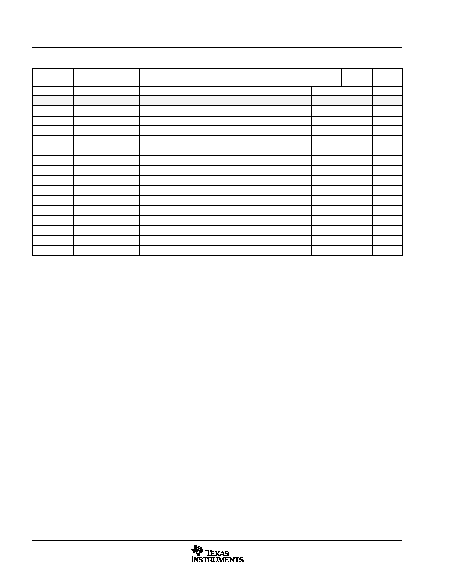
Functional Overview
84
August 2002 - Revised August 2004
SPRS197D
Table 3-27. USB Function Registers (Continued)
BYTE
ADDRESS
RESET
VALUE
ACCESS
TYPE
ACCESS
WIDTH
DESCRIPTION
REGISTER NAME
FFFB:40BC
EP15_RX
Receive Endpoint Configuration 15 Register
16
RW
undef
FFFB:40C0
Reserved
FFFB:40C4
EP1_TX
Transmit Endpoint Configuration 1 Register
16
RW
undef
FFFB:40C8
EP2_TX
Transmit Endpoint Configuration 2 Register
16
RW
undef
FFFB:40CC
EP3_TX
Transmit Endpoint Configuration 3 Register
16
RW
undef
FFFB:40D0
EP4_TX
Transmit Endpoint Configuration 4 Register
16
RW
undef
FFFB:40D4
EP5_TX
Transmit Endpoint Configuration 5 Register
16
RW
undef
FFFB:40D8
EP6_TX
Transmit Endpoint Configuration 6 Register
16
RW
undef
FFFB:40DC
EP7_TX
Transmit Endpoint Configuration 7 Register
16
RW
undef
FFFB:40E0
EP8_TX
Transmit Endpoint Configuration 8 Register
16
RW
undef
FFFB:40E4
EP9_TX
Transmit Endpoint Configuration 9 Register
16
RW
undef
FFFB:40E8
EP10_TX
Transmit Endpoint Configuration 10 Register
16
RW
undef
FFFB:40EC
EP11_TX
Transmit Endpoint Configuration 11 Register
16
RW
undef
FFFB:40F0
EP12_TX
Transmit Endpoint Configuration 12 Register
16
RW
undef
FFFB:40F4
EP13_TX
Transmit Endpoint Configuration 13 Register
16
RW
undef
FFFB:40F8
EP14_TX
Transmit Endpoint Configuration 14 Register
16
RW
undef
FFFB:40FC
EP15_TX
Transmit Endpoint Configuration 15 Register
16
RW
undef
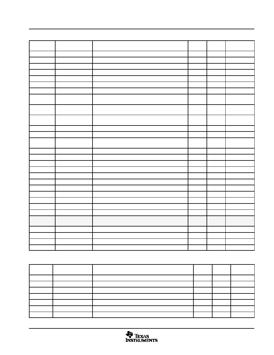
Functional Overview
85
August 2002 - Revised August 2004
SPRS197D
Table 3-28. USB Host Controller Registers
BYTE
ADDRESS
REGISTER NAME
DESCRIPTION
ACCESS
WIDTH
ACCESS
TYPE
RESET VALUE
FFFB:A000
HcRevision
OHCI Revision Register
32
R
0000 0010h
FFFB:A004
HcControl
Host Controller Operating Mode Register
32
RW
0000 0000h
FFFB:A008
HcCommandStatus
Host Controller Command and Status Register
32
RW
0000 0000h
FFFB:A00C
HcInterruptStatus
Host Controller Interrupt Status Register
32
RW
0000 0000h
FFFB:A010
HcInterruptEnable
Host Controller Interrupt Enable Register
32
RW
0000 0000h
FFFB:A014
HcInterruptDisable
Host Controller Interrupt Disable Register
32
R
0000 0000h
FFFB:A018
HcHCCA
LB Virtual Address HCCA Register
32
RW
0000 0000h
FFFB:A01C
HcPeriodCurrentED
LB Virtual Address Current Periodic EP Descriptor
Register
32
RW
0000 0000h
FFFB:A020
HcControlHeadED
LB Virtual Address Control EP Descriptor List Head
Register
32
RW
0000 0000h
FFFB:A024
HcControlCurrentED
LB Virtual Address Current Control EP Descriptor
Register
32
RW
0000 0000h
FFFB:A028
HcBulkHeadED
LB Virtual Address Bulk EP Descriptor List Head Register
32
RW
0000 0000h
FFFB:A02C
HcBulkCurrentED
LB Virtual Address Current Bulk EP Descriptor Register
32
RW
0000 0000h
FFFB:A030
HcDoneHead
LB Virtual Address Retired Transfer Descriptor List Head
Register
32
R
undef
FFFB:A034
HcFmInterval
Frame Interval Register
32
RW
0000 2EDFh
FFFB:A038
HcFmRemaining
Remaining Frame Time Register
32
R
0000 0000h
FFFB:A03C
HcFmNumber
Remaining Frame Number Register
32
R
0000 0000h
FFFB:A040
HcPeriodicStart
Periodic Start Time Register
32
RW
0000 0000h
FFFB:A044
HcLSThreshold
Low Speed Start Threshold Register
32
RW
0000 0628h
FFFB:A048
HcRhDescriptorA
USB Root Hub Descriptor Register A
32
RW
0A00 1203h
FFFB:A04C
HcRhDescriptorB
USB Root Hub Descriptor Register B
32
RW
0000 0000h
FFFB:A050
HcRhStatus
USB Root Hub Status Register
32
RW
0000 0000h
FFFB:A054
HcRhPortStatus1
Port 1 Control and Status Register
32
RW
0000 0100h
FFFB:A058
HcRhPortStatus2
Port 2 Control and Status Register
32
RW
0000 0100h
FFFB:A05C
HcRhPortStatus3
Port 3 Control and Status Register
32
RW
0000 0100h
FFFB:A060 -
FFFB:A0DC
Reserved
FFFB:A0E0
HostUEAddr
LB Virtual Address Last Unrecoverable Error Register
32
R
0000 0000h
FFFB:A0E4
HostUEStatus
LB Cycle Type Last Unrecoverable Error Register
32
R
0000 0000h
FFFB:A0E8
HostTimeoutCtrl
USB Host Mastered Local Bus Time-out Enable Register
32
RW
0000 0000h
FFFB:A0EC
HostRevision
USB Host Controller Revision Register
32
R
-
Table 3-29. Camera Interface Registers
BYTE
ADDRESS
REGISTER NAME
DESCRIPTION
ACCESS
WIDTH
ACCESS
TYPE
RESET
VALUE
FFFB:6800
CTRLCLOCK
Clock Control Register
32
RW
0000 0000h
FFFB:6804
IT_STATUS
Interrupt Status Register
32
R
0000 0000h
FFFB:6808
MODE
Mode Configuration Register
32
RW
0000 0200h
FFFB:680C
STATUS
Status Register
32
R
0000 0000h
FFFB:6810
CAMDATA
Image Data Register
32
R
0000 0000h
FFFB:6814
GPIO
GPIO Register
32
RW
0000 0000h
FFFB:6818
PEAK_COUNTER
Fifo Peak Counter Register
32
RW
0000 0000h

Functional Overview
86
August 2002 - Revised August 2004
SPRS197D
Table 3-30. MPU I/O/Keyboard Registers
BYTE
ADDRESS
REGISTER NAME
DESCRIPTION
ACCESS
WIDTH
ACCESS
TYPE
RESET
VALUE
FFFB:5000
INPUT_LATCH
Input Register
16
R
undef
FFFB:5004
OUTPUT_REG
Output Register
16
RW
undef
FFFB:5008
IO_CNTL
Input Output Control Register
16
RW
FFFFh
FFFB:500C
Reserved
FFFB:5010
KBR_LATCH
Keyboard Row Inputs Register
16
R
undef
FFFB:5014
KBC_REG
Keyboard Column Outputs Register
16
RW
0000h
FFFB:5018
GPIO_EVENT_MODE GPIO Event Mode Register
16
RW
0000h
FFFB:501C
GPIO_INT_EDGE
GPIO Interrupt Edge Register
16
RW
0000h
FFFB:5020
KBD_INT
Keyboard Interrupt Register
16
R
0000h
FFFB:5024
GPIO_INT
GPIO Interrupt Register
16
R
0000h
FFFB:5028
KBD_MASKIT
Keyboard Mask Interrupt Register
16
RW
0000h
FFFB:502C
GPIO_MASKIT
GPIO Mask Interrupt Register
16
RW
0000h
FFFB:5030
GPIO_DEBOUNCING
GPIO Debouncing Register
16
RW
0000h
FFFB:5034
GPIO_LATCH
GPIO Latch Register
16
R
0000h
Table 3-31. PWL Registers
BYTE
ADDRESS
REGISTER NAME
DESCRIPTION
ACCESS
WIDTH
ACCESS
TYPE
RESET
VALUE
FFFB:5800
PWL_LEVEL
PWL Level Register
8
RW
0000h
FFFB:5804
PWL_CTRL
PWL Control Register
8
RW
0000h
Table 3-32. PWT Registers
BYTE
ADDRESS
REGISTER NAME
DESCRIPTION
ACCESS
WIDTH
ACCESS
TYPE
RESET
VALUE
FFFB:6000
PWT_FRC
PWT Frequency Control Register
8
RW
0000h
FFFB:6004
PWT_VCR
PWT Volume Control Register
8
RW
0000h
FFFB:6008
PWT_GCR
PWT General Control Register
8
RW
0000h
Table 3-33. LED Pulse Generator 1 Registers
BYTE
ADDRESS
REGISTER NAME
DESCRIPTION
ACCESS
WIDTH
ACCESS
TYPE
RESET
VALUE
FFFB:D000
LCR_1
LPG1 Control Register
8
RW
00h
FFFB:D004
PMR_1
LPG1 Power Management Register
8
RW
00h
Table 3-34. LED Pulse Generator 2 Registers
BYTE
ADDRESS
REGISTER NAME
DESCRIPTION
ACCESS
WIDTH
ACCESS
TYPE
RESET
VALUE
FFFB:D800
LCR_2
LPG2 Control Register
8
RW
00h
FFFB:D804
PMR_2
LPG2 Power Management Register
8
RW
00h
Table 3-35. 32k Timer Registers
BYTE ADDRESS
REGISTER
NAME
DESCRIPTION
ACCESS
WIDTH
ACCESS
TYPE
RESET
VALUE
FFFB:9000
TVR
Tick Value Register
32
RW
00FF FFFFh
FFFB:9004
TCR
Tick Counter Register
32
R
00FF FFFFh
FFFB:9008
CR
Control Register
32
RW
0000 0008h

Functional Overview
87
August 2002 - Revised August 2004
SPRS197D
Table 3-36. Real-Time Clock Registers
BYTE
ADDRESS
REGISTER NAME
DESCRIPTION
ACCESS
WIDTH
ACCESS
TYPE
RESET
VALUE
FFFB:4800
SECONDS_REG
RTC Seconds Register
8
RW
00h
FFFB:4804
MINUTES_REG
RTC Minutes Register
8
RW
00h
FFFB:4808
HOURS_REG
RTC Hours Register
8
RW
00h
FFFB:480C
DAYS_REG
RTC Days Register
8
RW
01h
FFFB:4810
MONTHS_REG
RTC Months Register
8
RW
01h
FFFB:4814
YEARS_REG
RTC Years Register
8
RW
00h
FFFB:4818
WEEK_REG
RTC Day of the Week Register
8
RW
00h
FFFB:481C
Reserved
FFFB:4820
ALARM_SECOND_REG
RTC Alarm Seconds Register
8
RW
00h
FFFB:4824
ALARM_MINUTES_REG
RTC Alarm Minutes Register
8
RW
00h
FFFB:4828
ALARM_HOURS_REG
RTC Alarm Hours Register
8
RW
00h
FFFB:482C
ALARM_DAYS_REG
RTC Alarm Days Register
8
RW
01h
FFFB:4830
ALARM_MONTHS_REG
RTC Alarm Months Register
8
RW
01h
FFFB:4834
ALARM_YEARS_REG
RTC Alarm Years Register
8
RW
00h
FFFB:4838 -
FFFB:483C
Reserved
FFFB:4840
RTC_CTRL_REG
RTC Control Register
8
RW
00h
FFFB:4844
RTC_STATUS_REG
RTC Status Register
8
RW
00h
FFFB:4848
RTC_INTERRUPTS_REG
RTC Interrupts Register
8
RW
00h
FFFB:484C
RTC_COMP_LSB_REG
RTC Compensation LSB Register
8
RW
00h
FFFB:4850
RTC_COMP_MSB_REG
RTC Compensation MSB Register
8
RW
00h
Table 3-37. Frame Adjustment Counter Registers
BYTE
ADDRESS
REGISTER NAME
DESCRIPTION
ACCESS
WIDTH
ACCESS
TYPE
RESET
VALUE
FFFB:A800
FARC
Frame Adjustment Reference Count Register
16
RW
0000h
FFFB:A804
FSC
Frame Start Count Register
16
R
0000h
FFFB:A808
CTRL
Control and Configuration Register
16
RW
0000h
FFFB:A80C
STATUS
Status Register
16
R
0000h
FFFB:A810
SYNC_CNT
Frame Synchronization Register
16
R
undef
FFFB:A814
START_CNT
Frame Start Counter Register
16
R
undef

Functional Overview
88
August 2002 - Revised August 2004
SPRS197D
3.15.3
MPU Configuration Registers
The MPU Configuration Registers include the following:
�
Pin Multiplexing Setup:
-
OMAP5910 Pin Configuration Registers
�
Local Bus and MMU Setup:
-
Local Bus Control Registers
-
Local Bus MMU Registers
-
DSP MMU Registers
�
MPUI and TIPB Setup:
-
MPU Interface (MPUI) Registers
-
TIPB (Private) Bridge 1 Configuration Registers
-
TIPB (Public) Bridge 2 Configuration Registers
-
MPU UART TI Peripheral Bus Switch Registers
-
Traffic Controller Registers
�
Clock and Power Management:
-
MPU Clock/Reset/Power Mode Control Registers
-
DPLL1 Configuration Register
-
Ultra Low-Power Device Module Registers
�
Device Identification:
-
Device Die Identification Registers
-
JTAG Identification Code Register
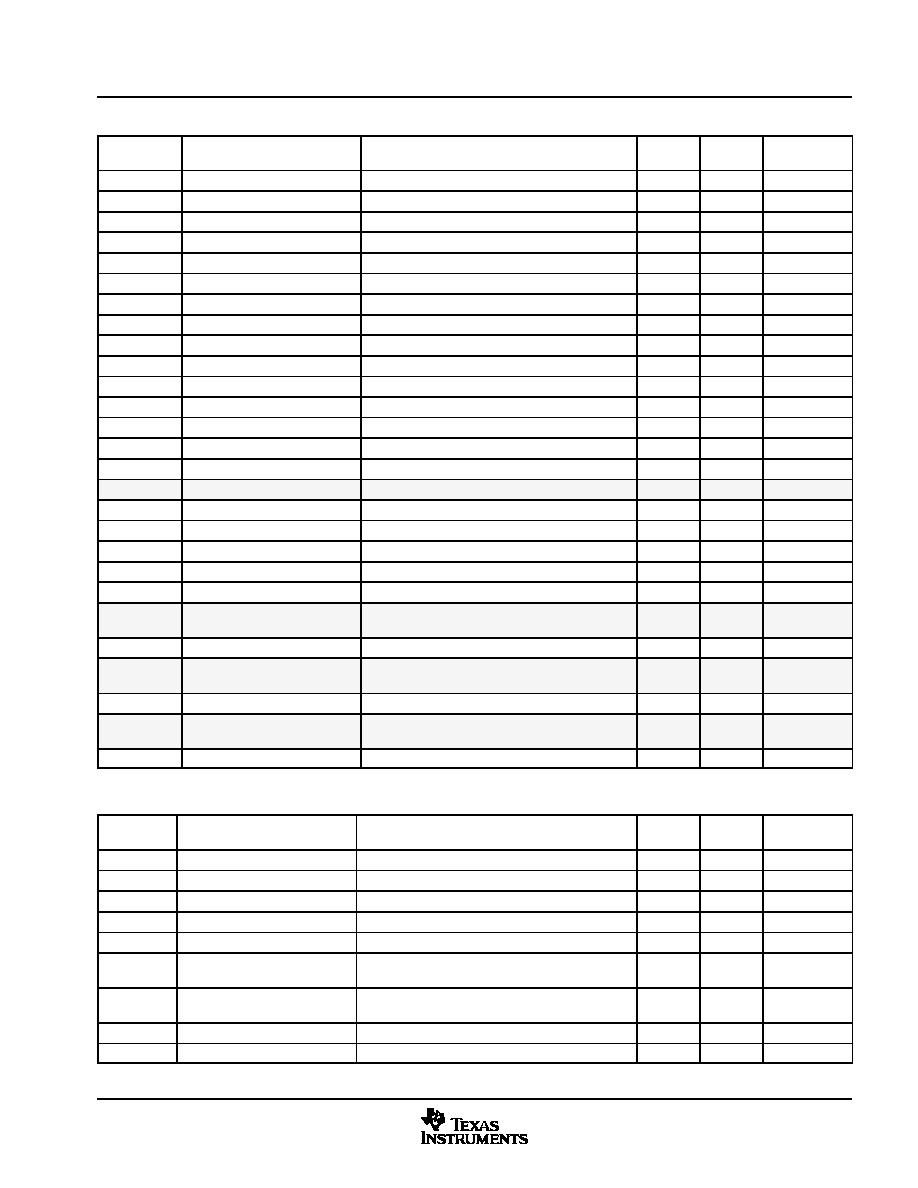
Functional Overview
89
August 2002 - Revised August 2004
SPRS197D
Table 3-38. OMAP 5910 Pin Configuration Registers
BYTE
ADDRESS
REGISTER NAME
DESCRIPTION
ACCESS
WIDTH
ACCESS
TYPE
RESET
VALUE
FFFE:1000
FUNC_MUX_CTRL_0
Functional Multiplexing Control 0 Register
32
RW
0000 0000h
FFFE:1004
FUNC_MUX_CTRL_1
Functional Multiplexing Control 1 Register
32
RW
0000 0000h
FFFE:1008
FUNC_MUX_CTRL_2
Functional Multiplexing Control 2 Register
32
RW
0000 0000h
FFFE:100C
COMP_MODE_CTRL_0
Compatibility Mode Control 0 Register
32
RW
0000 0000h
FFFE:1010
FUNC_MUX_CTRL_3
Functional Multiplexing Control 3 Register
32
RW
0000 0000h
FFFE:1014
FUNC_MUX_CTRL_4
Functional Multiplexing Control 4 Register
32
RW
0000 0000h
FFFE:1018
FUNC_MUX_CTRL_5
Functional Multiplexing Control 5 Register
32
RW
0000 0000h
FFFE:101C
FUNC_MUX_CTRL_6
Functional Multiplexing Control 6 Register
32
RW
0000 0000h
FFFE:1020
FUNC_MUX_CTRL_7
Functional Multiplexing Control 7 Register
32
RW
0000 0000h
FFFE:1024
FUNC_MUX_CTRL_8
Functional Multiplexing Control 8 Register
32
RW
0000 0000h
FFFE:1028
FUNC_MUX_CTRL_9
Functional Multiplexing Control 9 Register
32
RW
0000 0000h
FFFE:102C
FUNC_MUX_CTRL_A
Functional Multiplexing Control A Register
32
RW
0000 0000h
FFFE:1030
FUNC_MUX_CTRL_B
Functional Multiplexing Control B Register
32
RW
0000 0000h
FFFE:1034
FUNC_MUX_CTRL_C
Functional Multiplexing Control C Register
32
RW
0000 0000h
FFFE:1038
FUNC_MUX_CTRL_D
Functional Multiplexing Control D Register
32
RW
0000 0000h
FFFE:103C
Reserved
FFFE:1040
PULL_DWN_CTRL_0
Pulldown Control 0 Register
32
RW
0000 0000h
FFFE:1044
PULL_DWN_CTRL_1
Pulldown Control 1 Register
32
RW
0000 0000h
FFFE:1048
PULL_DWN_CTRL_2
Pulldown Control 2 Register
32
RW
0000 0000h
FFFE:104C
PULL_DWN_CTRL_3
Pulldown Control 3 Register
32
RW
0000 0000h
FFFE:1050
GATE_INH_CTRL_0
Gate and Inhibit Control 0 Register
32
RW
0000 0000h
FFFE:1054 -
FFFE:105C
Reserved
FFFE:1060
VOLTAGE_CTRL_0
Voltage Control 0 Register
32
RW
0000 0000h
FFFE:1064 -
FFFE:106C
Reserved
FFFE:1070
TEST_DBG_CTRL_0
Test Debug Control 0 Register
32
RW
0000 0000h
FFFE:1074 -
FFFE:107C
Reserved
FFFE:1080
MOD_CONF_CTRL_0
Module Configuration Control 0 Register
32
RW
0000 0000h
Table 3-39. Local Bus Control Registers
BYTE
ADDRESS
REGISTER NAME
DESCRIPTION
ACCESS
WIDTH
ACCESS
TYPE
RESET
VALUE
FFFE:C100
LB_MPU_TIMEOUT
Local Bus MPU Access TIMEOUT
32
RW
0000 00FFh
FFFE:C104
LB_HOLD_TIMER
Local Bus Hold Timer
32
RW
0000 0000h
FFFE:C108
LB_PRIORITY_REG
Local Bus MPU Access Priority
32
RW
0000 0000h
FFFE:C10C
LB_CLOCK_DIV
Local Bus Clock Divider
32
RW
0000 00FCh
FFFE:C110
LB_ABORT_ADD
Local Bus Address Of Aborted MPU Cycle
32
R
FFFF FFFFh
FFFE:C114
LB_ABORT_DATA
Local Bus Cycle Data Of Aborted MPU Write
Cycle
32
R
FFFF FFFFh
FFFE:C118
LB_ABORT_STATUS
Local Bus Cycle Type Of Aborted MPU Write
Cycle
32
R
0000 0000h
FFFE:C11C
LB_IRQ_OUTPUT
LocaL Bus External Interrupt Output Control
32
RW
0000 0000h
FFFE:C120
LB_IRQ_INPUT
Local Bus External Interrupt Status
32
RW
0000 0000h
Functional Overview
90
August 2002 - Revised August 2004
SPRS197D
Table 3-40. Local Bus MMU Registers
BYTE
ADDRESS
REGISTER NAME
DESCRIPTION
ACCESS
WIDTH
ACCESS
TYPE
RESET
VALUE
FFFE:C204
LB_MMU_WALKING_ST_REG
Local Bus MMU Walking Status
32
RW
0000h
FFFE:C208
LB_MMU_CNTL_REG
Local Bus MMU Control
32
RW
0000h
FFFE:C20C
LB_MMU_FAULT_AD_H_REG
Local Bus MMU Fault Address High
32
R
0000h
FFFE:C210
LB_MMU_FAULT_AD_L_REG
Local Bus MMU Fault Address Low
32
R
0000h
FFFE:C214
LB_MMU_FAULT_ST_REG
Local Bus MMU Fault Status
32
R
0000h
FFFE:C218
LB_MMU_IT_ACK_REG
Local Bus MMU Interrupt Acknowledge
32
W
0000h
FFFE:C21C
LB_MMU_TTB_H_REG
Local Bus MMU TTB Register High
32
RW
0000h
FFFE:C220
LB_MMU_TTB_L_REG
Local Bus MMU TTB Register Low
32
RW
0000h
FFFE:C224
LB_MMU_LOCK_REG
Local Bus MMU Lock Counter
32
RW
0000h
FFFE:C228
LB_MMU_LD_TLB_REG
Local Bus MMU TLB Load/Read Control
32
RW
0000h
FFFE:C22C
LB_MMU_CAM_H_REG
Local Bus MMU CAM Entry High
32
RW
0000h
FFFE:C230
LB_MMU_CAM_L_REG
Local Bus MMU CAM Entry Low
32
RW
0000h
FFFE:C234
LB_MMU_RAM_H_REG
Local Bus MMU RAM Entry High
32
RW
0000h
FFFE:C238
LB_MMU_RAM_L_REG
Local Bus MMU RAM Entry Low
32
RW
0000h
FFFE:C23C
LB_MMU_GFLUSH_REG
Local Bus MMU Global Flush Control
32
RW
0000h
FFFE:C240
LB_MMU_FLUSH_ENTRY_REG
Local Bus MMU Individual Entry Flush
Control
32
RW
0000h
FFFE:C244
LB_MMU_READ_CAM_H_REG
Local Bus MMU CAM Read High
32
RW
0000h
FFFE:C248
LB_MMU_READ_CAM_L_REG
Local Bus MMU CAM Read Low
32
RW
0000h
FFFE:C24C
LB_MMU_READ_RAM_H_REG
Local Bus MMU RAM Read High
32
RW
0000h
FFFE:C250
LB_MMU_READ_RAM_L_REG
Local Bus MMU RAM Read Low
32
RW
0000h
Write access in ARM supervisor mode only.
Functional Overview
91
August 2002 - Revised August 2004
SPRS197D
Table 3-41. DSP MMU Registers
BYTE
ADDRESS
REGISTER NAME
DESCRIPTION
ACCESS
WIDTH
ACCESS
TYPE
RESET
VALUE
FFFE:D200
DSP_MMU_PREFETCH_REG
DSP MMU Prefetch Register
32
RW
0000h
FFFE:D204
DSP_MMU_WALKING_ST_REG
DSP MMU Prefetch Status Register
32
R
0000h
FFFE:D208
DSP_MMU_CNTL_REG
DSP MMU Control Register
32
RW
0000h
FFFE:D20C
DSP_MMU_FAULT_AD_H_REG
DSP MMU Fault Address Register MSB
32
R
0000h
FFFE:D210
DSP_MMU_FAULT_AD_L_REG
DSP MMU Fault Address Register LSB
32
R
0000h
FFFE:D214
DSP_MMU_F_ST_REG
DSP MMU Fault Status Register
32
R
0000h
FFFE:D218
DSP_MMU_IT_ACK_REG
DSP MMU IT Acknowledge Register
32
W
0000h
FFFE:D21C
DSP_MMU_TTB_H_REG
DSP MMU TTB Register MSB
32
RW
0000h
FFFE:D220
DSP_MMU_TTB_L_REG
DSP MMU TTB Register LSB
32
RW
0000h
FFFE:D224
DSP_MMU_LOCK_REG
DSP MMU Lock Counter Register
32
RW
0000h
FFFE:D228
DSP_MMU_LD_TLB_REG
DSP MMU Load Entry TLB Register
32
RW
0000h
FFFE:D22C
DSP_MMU_CAM_H_REG
DSP MMU CAM Entry Register MSB
32
RW
0000h
FFFE:D230
DSP_MMU_CAM_L_REG
DSP MMU CAM Entry Register LSB
32
RW
0000h
FFFE:D234
DSP_MMU_RAM_H_REG
DSP MMU RAM Entry Register MSB
32
RW
0000h
FFFE:D238
DSP_MMU_RAM_L_REG
DSP MMU RAM Entry Register LSB
32
RW
0000h
FFFE:D23C
DSP_MMU_GFLUSH_REG
DSP MMU Global Flush Register
32
RW
0000h
FFFE:D240
DSP_MMU_FLUSH_ENTRY_REG
DSP MMU Individual Flush Register
32
RW
0000h
FFFE:D244
DSP_MMU_READ_CAM_H_REG
DSP MMU Read CAM Register MSB
32
RW
0000h
FFFE:D248
DSP_MMU_READ_CAM_L_REG
DSP MMU Read CAM Register LSB
32
RW
0000h
FFFE:D24C
DSP_MMU_READ_RAM_H_REG
DSP MMU Read RAM Register MSB
32
RW
0000h
FFFE:D250
DSP_MMU_READ_RAM_L_REG
DSP MMU Read RAM Register LSB
32
RW
0000h
Table 3-42. MPUI Registers
BYTE
ADDRESS
REGISTER NAME
DESCRIPTION
ACCESS
WIDTH
ACCESS
TYPE
RESET
VALUE
FFFE:C900
CTRL_REG
MPUI Control Register
32
RW
0003 FF1Bh
FFFE:C904
DEBUG_ADDR
MPUI Debug Address Register
32
R
01FF FFFFh
FFFE:C908
DEBUG_DATA
MPUI Debug Data Register
32
R
FFFF FFFFh
FFFE:C90C
DEBUG_FLAG
MPUI Debug Flag Register
32
R
0800h
FFFE:C910
STATUS_REG
MPUI Status Register
32
R
0000h
FFFE:C914
DSP_STATUS_REG
MPUI DSP Status Register
32
R
undef
FFFE:C918
DSP_BOOT_CONFIG
MPUI Boot Configuration Register
32
RW
0000h
FFFE:C91C
DSP_MPUI_CONFIG
MPUI DSP MPUI Configuration Register
32
RW
FFFFh
Table 3-43. TIPB (Private) Bridge 1 Configuration Registers
BYTE
ADDRESS
REGISTER NAME
DESCRIPTION
ACCESS
WIDTH
ACCESS
TYPE
RESET
VALUE
FFFE:CA00
TIPB_CNTL
Private TIPB Control Register
32
RW
FF11h
FFFE:CA04
TIPB_BUS_ALLOC
Private TIPB Bus Allocation Register
32
RW
0009h
FFFE:CA08
MPU_TIPB_CNTL
Private MPU TIPB Control Register
32
RW
0000h
FFFE:CA0C ENHANCED_TIPB_CNTL
Private Enhanced TIPB Control Register
32
RW
0007h
FFFE:CA10
ADDRESS_DBG
Private Debug Address Register
32
R
FFFFh
FFFE:CA14
DATA_DEBUG_LOW
Private Debug Data LSB Register
32
R
FFFFh
FFFE:CA18
DATA_DEBUG_HIGH
Private Debug Data MSB Register
32
R
FFFFh
FFFE:CA1C DEBUG_CNTR_SIG
Private Debug Control Signals Register
32
R
00F8h

Functional Overview
92
August 2002 - Revised August 2004
SPRS197D
Table 3-44. TIPB (Public) Bridge 2 Configuration Registers
BYTE
ADDRESS
REGISTER NAME
DESCRIPTION
ACCESS
WIDTH
ACCESS
TYPE
RESET
VALUE
FFFE:D300
TIPB_CNTL
Public TIPB Control Register
16
RW
FF11h
FFFE:D304
TIPB_BUS_ALLOC
Public TIPB Bus Allocation Register
16
RW
0009h
FFFE:D308
MPU_TIPB_CNTL
Public MPU TIPB Control Register
16
RW
0000h
FFFE:D30C
ENHANCED_TIPB_CNTL
Public Enhanced TIPB Control Register
16
RW
0007h
FFFE:D310
ADDRESS_DBG
Public Debug Address Register
16
R
FFFFh
FFFE:D314
DATA_DEBUG_LOW
Public Debug Data LSB Register
16
R
FFFFh
FFFE:D318
DATA_DEBUG_HIGH
Public Debug Data MSB Register
16
R
FFFFh
FFFE:D31C
DEBUG_CNTR_SIG
Public Debug Control Signals Register
16
R
00F8h
Table 3-45. MPU UART TIPB Bus Switch Registers
BYTE
ADDRESS
REGISTER NAME
DESCRIPTION
ACCESS
WIDTH
ACCESS
TYPE
RESET
VALUE
FFFB:C800
RHSW_ARM_CNF1
UART1 TIPB Switch Configuration Register (MPU)
16
RW
0001h
FFFB:C804
RHSW_ARM_STA1
UART1 TIPB Switch Status Register (MPU)
16
R
0001h
FFFB:C808 -
FFFB:C83C
Reserved
FFFB:C840
RHSW_ARM_CNF2 UART2 TIPB Switch Configuration Register (MPU)
16
RW
0001h
FFFB:C844
RHSW_ARM_STA2
UART2 TIPB Switch Status Register (MPU)
16
R
0001h
FFFB:C848 -
FFFB:C87C
Reserved
FFFB:C880
RHSW_ARM_CNF3 UART3 TIPB Switch Configuration Register (MPU)
16
RW
0001h
FFFB:C884
RHSW_ARM_STA3
UART3 TIPB Switch Status Register (MPU)
16
R
0001h

Functional Overview
93
August 2002 - Revised August 2004
SPRS197D
Table 3-46. Traffic Controller Registers
BYTE
ADDRESS
REGISTER NAME
DESCRIPTION
ACCESS
WIDTH
ACCESS
TYPE
RESET
VALUE
FFFE:CC00
IMIF_PRIO
TC IMIF Priority Register
32
RW
0000 0000h
FFFE:CC04
EMIFS_PRIO_REG
TC EMIFS Priority Register
32
RW
0000 0000h
FFFE:CC08
EMIFF_PRIO_REG
TC EMIFF Priority Register
32
RW
0000 0000h
FFFE:CC0C EMIFS_CONFIG_REG
TC EMIFS Configuration Register
32
RW
y00z0b
FFFE:CC10
EMIFS_CS0_CONFIG
TC EMIFS CS0 Configuration Register
32
RW
0010 FFFBh
FFFE:CC14
EMIFS_CS1_CONFIG
TC EMIFS CS1 Configuration Register
32
RW
0010 FFFBh
FFFE:CC18
EMIFS_CS2_CONFIG
TC EMIFS CS2 Configuration Register
32
RW
0010 FFFBh
FFFE:CC1C EMIFS_CS3_CONFIG
TC EMIFS CS3 Configuration Register
32
RW
0010 FFFBh
FFFE:CC20
EMIFF_SDRAM_CONFIG
TC EMIFF SDRAM Configuration Register
32
RW
0061 8800h
FFFE:CC24
EMIFF_MRS
TC EMIFF SDRAM MRS Register
32
RW
0000 0037h
FFFE:CC28
TIMEOUT1
TC Timeout 1 Register
32
RW
0000 0000h
FFFE:CC2C TIMEOUT2
TC Timeout 2 Register
32
RW
0000 0000h
FFFE:CC30
TIMEOUT3
TC Timeout 3 Register
32
RW
0000 0000h
FFFE:CC34
ENDIANISM
TC Endianism Register
32
RW
0000 0000h
FFFE:CC38
Reserved
32
RW
0000 0000h
FFFE:CC3C EMIFF_SDRAM_CONFIG_2
TC EMIFF SDRAM Configuration Register 2
32
RW
0000 0003h
FFFE:CC40
EMIFS_CFG_DYN_WAIT
TC EMIFS Wait-State Configuration Register
32
RW
0000 0000h
The value of y is dependent upon the state of the FLASH.RDY pin and the value of z is dependent upon the state of the MPU_BOOT pin upon
power-on reset.
Table 3-47. MPU Clock/Reset/Power Mode Control Registers
BYTE
ADDRESS
REGISTER NAME
DESCRIPTION
ACCESS
WIDTH
ACCESS
TYPE
RESET
VALUE
FFFE:CE00
ARM_CKCTL
MPU Clock Control Register
32
RW
3000h
FFFE:CE04
ARM_IDLECT1
MPU Idle Control 1 Register
32
RW
0400h
FFFE:CE08
ARM_IDLECT2
MPU Idle Control 2 Register
32
RW
0100h
FFFE:CE0C ARM_EWUPCT
MPU External Wakeup Control Register
32
RW
003Fh
FFFE:CE10
ARM_RSTCT1
MPU Reset Control 1 Register
32
RW
0000h
FFFE:CE14
ARM_RSTCT2
MPU Reset Control 2 Register
32
RW
0000h
FFFE:CE18
ARM_SYSST
MPU System Status Register
32
RW
0038h
Table 3-48. DPLL1 Register
BYTE
ADDRESS
REGISTER NAME
DESCRIPTION
ACCESS
WIDTH
ACCESS
TYPE
RESET
VALUE
FFFE:CF00
DPLL1_CTL_REG
DPLL1 Control Register
32
RW
0000 2002h

Functional Overview
94
August 2002 - Revised August 2004
SPRS197D
Table 3-49. Ultra Low-Power Device Module Registers
BYTE
ADDRESS
REGISTER NAME
DESCRIPTION
ACCESS
WIDTH
ACCESS
TYPE
RESET
VALUE
FFFE:0800
COUNTER_32_LSB
ULPD 32-kHz Counter Register LSB
16
R
0001h
FFFE:0804
COUNTER_32_MSB
ULPD 32-kHz Counter Register MSB
16
R
0001h
FFFE:0808
COUNTER_HIGH_FREQ_LSB
ULPD High-Frequency Counter LSB Register
16
R
0001h
FFFE:080C
COUNTER_HIGH_FREQ_MSB
ULPD High-Frequency Counter MSB Register
16
R
0000h
FFFE:0810
GAUGING_CTRL_REG
ULPD Gauging Control Register
16
RW
0000h
FFFE:0814
IT_STATUS_REG
ULPD Interrupt Status Register
16
R
0000h
FFFE:0818 -
FFFE:0820
Reserved
FFFE:0824
SETUP_ULPD1_REG
ULPD Wakeup Time Setup Register
16
RW
03FFh
FFFE:0828 -
FFFE:082C
Reserved
FFFE:0830
CLOCK_CTRL_REG
ULPD Clock Control Register
16
RW
0000h
FFFE:0834
SOFT_REQ_REG
ULPD Soft Clock Request Register
16
RW
0000h
FFFE:0838
COUNTER_32_FIQ_REG
ULPD Modem Shutdown Delay Register
16
RW
0001h
FFFE:083C
DPLL_CTRL_REG
ULPD USB DPLL Control Register
16
RW
2211h
FFFE:0840
STATUS_REQ_REG
ULPD Hardware Request Status Register
16
RW
undef
FFFE:0844
Reserved
FFFE:0848
LOCK_TIME_REG
ULPD APLL Lock Time Register
16
RW
0960h
FFFE:084C
APLL_CTRL_REG
ULPD APLL Control Register
16
RW
undef
FFFE:0850
POWER_CTRL_REG
ULPD Power Control Register
16
RW
0008h
Table 3-50. Device Die Identification Registers
BYTE
ADDRESS
REGISTER NAME
DESCRIPTION
ACCESS
WIDTH
ACCESS
TYPE
RESET
VALUE
FFFE:1800
DIE_ID_LSB
Device Die Identification Register (LSB)
32
R
-
FFFE:1804
DIE_ID_MSB
Device Die Identification Register (MSB)
32
R
-
Table 3-51. JTAG Identification Code Register
BYTE
ADDRESS
REGISTER NAME
DESCRIPTION
ACCESS
WIDTH
ACCESS
TYPE
RESET
VALUE
FFFE:D404
JTAG_ID
JTAG Identification Code Register
32
R
-

Functional Overview
95
August 2002 - Revised August 2004
SPRS197D
3.16 DSP Register Descriptions
The following tables describe the DSP registers including register addresses, descriptions, required access
widths, access types (R-read, W-write, RW-read/write) and reset values. These tables are organized by
function with like peripherals or functions together and are therefore not necessarily in the order of ascending
register addresses.
NOTE: All accesses to these registers must be of the data access widths indicated to avoid
a TIPB bus error condition and a corresponding interrupt. Reserved addresses should never
be accessed
3.16.1
DSP Private Peripheral Registers
The DSP private peripheral registers include the following:
�
DMA Controller:
-
DSP DMA Controller Registers
�
Timers:
-
DSP Timer 1 Registers
-
DSP Timer 2 Registers
-
DSP Timer 3 Registers
-
DSP Watchdog Timer Registers
�
Interrupt Control:
-
DSP Interrupt Interface Registers
-
DSP Level 2 Interrupt Handler Registers

Functional Overview
96
August 2002 - Revised August 2004
SPRS197D
Table 3-52. DSP DMA Controller Registers
DSP WORD
ADDRESS
REGISTER NAME
DESCRIPTION
ACCESS
WIDTH
ACCESS
TYPE
RESET VALUE
0x00 0C00h
DMA_CSDP0
Channel 0 Source/Destination Parameters Register
16
RW
0000h
0x00 0C01h
DMA_CCR0
Channel 0 Control Register
16
RW
0000h
0x00 0C02h
DMA_CICR0
Channel 0 Interrupt Control Register
16
RW
0003h
0x00 0C03h
DMA_CSR0
Channel 0 Status Register
16
R
0000h
0x00 0C04h
DMA_CSSA_L0
Channel 0 Source Start Address Register LSB
16
RW
undef
0x00 0C05h
DMA_CSSA_U0
Channel 0 Source Start Address Register MSB
16
RW
undef
0x00 0C06h
DMA_CDSA_L0
Channel 0 Destination Start Address Register LSB
16
RW
undef
0x00 0C07h
DMA_CDSA_U0
Channel 0 Destination Start Address Register MSB
16
RW
undef
0x00 0C08h
DMA_CEN0
Channel 0 Element Number Register
16
RW
undef
0x00 0C09h
DMA_CFN0
Channel 0 Frame Number Register
16
RW
undef
0x00 0C0Ah
DMA_CSFI0
Channel 0 Frame Index Register
16
RW
undef
0x00 0C0Bh
DMA_CSEI0
Channel 0 Element Index Register
16
RW
undef
0x00 0C0Ch
DMA_CSAC0
Channel 0 Source Address Counter Register
16
RW
undef
0x00 0C0Dh
DMA_CDAC0
Channel 0 Destination Address Counter Register
16
RW
undef
0x00 0C0Eh
DMA_CDFI0
Channel 0 Destination Frame Index
16
RW
undef
0x00 0C0Fh
DMA_CDEI0
Channel 0 Destination Element Index
16
RW
undef
0x00 0C10h -
0x00 0C1Fh
Reserved
0x00 0C20h
DMA_CSDP1
Channel 1 Source/Destination Parameters Register
16
RW
0000h
0x00 0C21h
DMA_CCR1
Channel 1 Control Register
16
RW
0000h
0x00 0C22h
DMA_CICR1
Channel 1 Interrupt Control Register
16
RW
0003h
0x00 0C23h
DMA_CSR1
Channel 1 Status Register
16
R
0000h
0x00 0C24h
DMA_CSSA_L1
Channel 1 Source Start Address Register LSB
16
RW
undef
0x00 0C25h
DMA_CSSA_U1
Channel 1 Source Start Address Register MSB
16
RW
undef
0x00 0C26h
DMA_CDSA_L1
Channel 1 Destination Start Address Register LSB
16
RW
undef
0x00 0C27h
DMA_CDSA_U1
Channel 1 Destination Start Address Register MSB
16
RW
undef
0x00 0C28h
DMA_CEN1
Channel 1 Element Number Register
16
RW
undef
0x00 0C29h
DMA_CFN1
Channel 1 Frame Number Register
16
RW
undef
0x00 0C2Ah
DMA_CSFI1
Channel 1 Frame Index Register
16
RW
undef
0x00 0C2Bh
DMA_CSEI1
Channel 1 Element Index Register
16
RW
undef
0x00 0C2Ch
DMA_CSAC1
Channel 1 Source Address Counter Register
16
RW
undef
0x00 0C2Dh
DMA_CDAC1
Channel 1 Destination Address Counter Register
16
RW
undef
0x00 0C2Eh
DMA_CDFI1
Channel 1 Destination Frame Index
16
RW
undef
0x00 0C2Fh
DMA_CDEI1
Channel 1 Destination Element Index
16
RW
undef
0x00 0C30h -
0x00 0C3Fh
Reserved
0x00 0C40h
DMA_CSDP2
Channel 2 Source/Destination Parameters Register
16
RW
0000h
0x00 0C41h
DMA_CCR2
Channel 2 Control Register
16
RW
0000h
0x00 0C42h
DMA_CICR2
Channel 2 Interrupt Control Register
16
RW
0003h
0x00 0C43h
DMA_CSR2
Channel 2 Status Register
16
R
0000h
0x00 0C44h
DMA_CSSA_L2
Channel 2 Source Start Address Register LSB
16
RW
undef
0x00 0C45h
DMA_CSSA_U2
Channel 2 Source Start Address Register MSB
16
RW
undef
0x00 0C46h
DMA_CDSA_L2
Channel 2 Destination Start Address Register LSB
16
RW
undef
0x00 0C47h
DMA_CDSA_U2
Channel 2 Destination Start Address Register MSB
16
RW
undef

Functional Overview
97
August 2002 - Revised August 2004
SPRS197D
Table 3-52. DSP DMA Controller Registers (Continued)
DSP WORD
ADDRESS
RESET VALUE
ACCESS
TYPE
ACCESS
WIDTH
DESCRIPTION
REGISTER NAME
0x00 0C48h
DMA_CEN2
Channel 2 Element Number Register
16
RW
undef
0x00 0C49h
DMA_CFN2
Channel 2 Frame Number Register
16
RW
undef
0x00 0C4Ah
DMA_CSFI2
Channel 2 Frame Index Register
16
RW
undef
0x00 0C4Bh
DMA_CSEI2
Channel 2 Element Index Register
16
RW
undef
0x00 0C4Ch
DMA_CSAC2
Channel 2 Source Address Counter Register
16
RW
undef
0x00 0C4Dh
DMA_CDAC2
Channel 2 Destination Address Counter Register
16
RW
undef
0x00 0C4Eh
DMA_CDFI2
Channel 2 Destination Frame Index
16
RW
undef
0x00 0C4Fh
DMA_CDEI2
Channel 2 Destination Element Index
16
RW
undef
0x00 0C50h -
0x00 0C5Fh
Reserved
0x00 0C60h
DMA_CSDP3
Channel 3 Source/Destination Parameters Register
16
RW
0000h
0x00 0C61h
DMA_CCR3
Channel 3 Control Register
16
RW
0000h
0x00 0C62h
DMA_CICR3
Channel 3 Interrupt Control Register
16
RW
0003h
0x00 0C63h
DMA_CSR3
Channel 3 Status Register
16
R
0000h
0x00 0C64h
DMA_CSSA_L3
Channel 3 Source Start Address Register LSB
16
RW
undef
0x00 0C65h
DMA_CSSA_U3
Channel 3 Source Start Address Register MSB
16
RW
undef
0x00 0C66h
DMA_CDSA_L3
Channel 3 Destination Start Address Register LSB
16
RW
undef
0x00 0C67h
DMA_CDSA_U3
Channel 3 Destination Start Address Register MSB
16
RW
undef
0x00 0C68h
DMA_CEN3
Channel 3 Element Number Register
16
RW
undef
0x00 0C69h
DMA_CFN3
Channel 3 Frame Number Register
16
RW
undef
0x00 0C6Ah
DMA_CSFI3
Channel 3 Frame Index Register
16
RW
undef
0x00 0C6Bh
DMA_CSEI3
Channel 3 Element Index Register
16
RW
undef
0x00 0C6Ch
DMA_CSAC3
Channel 3 Source Address Counter Register
16
RW
undef
0x00 0C6Dh
DMA_CDAC3
Channel 3 Destination Address Counter Register
16
RW
undef
0x00 0C6Eh
DMA_CDFI3
Channel 3 Destination Frame Index
16
RW
undef
0x00 0C6Fh
DMA_CDEI3
Channel 3 Destination Element Index
16
RW
undef
0x00 0C70h -
0x00 0C7Fh
Reserved
0x00 0C80h
DMA_CSDP4
Channel 4 Source/Destination Parameters Register
16
RW
0000h
0x00 0C81h
DMA_CCR4
Channel 4 Control Register
16
RW
0000h
0x00 0C82h
DMA_CICR4
Channel 4 Interrupt Control Register
16
RW
0003h
0x00 0C83h
DMA_CSR4
Channel 4 Status Register
16
R
0000h
0x00 0C84h
DMA_CSSA_L4
Channel 4 Source Start Address Register LSB
16
RW
undef
0x00 0C85h
DMA_CSSA_U4
Channel 4 Source Start Address Register MSB
16
RW
undef
0x00 0C86h
DMA_CDSA_L4
Channel 4 Destination Start Address Register LSB
16
RW
undef
0x00 0C87h
DMA_CDSA_U4
Channel 4 Destination Start Address Register MSB
16
RW
undef
0x00 0C88h
DMA_CEN4
Channel 4 Element Number Register
16
RW
undef
0x00 0C89h
DMA_CFN4
Channel 4 Frame Number Register
16
RW
undef
0x00 0C8Ah
DMA_CSFI4
Channel 4 Frame Index Register
16
RW
undef
0x00 0C8Bh
DMA_CSEI4
Channel 4 Element Index Register
16
RW
undef
0x00 0C8Ch
DMA_CSAC4
Channel 4 Source Address Counter Register
16
RW
undef
0x00 0C8Dh
DMA_CDAC4
Channel 4 Destination Address Counter Register
16
RW
undef
0x00 0C8Eh
DMA_CDFI4
Channel 4 Destination Frame Index
16
RW
undef
0x00 0C8Fh
DMA_CDEI4
Channel 4 Destination Element Index
16
RW
undef
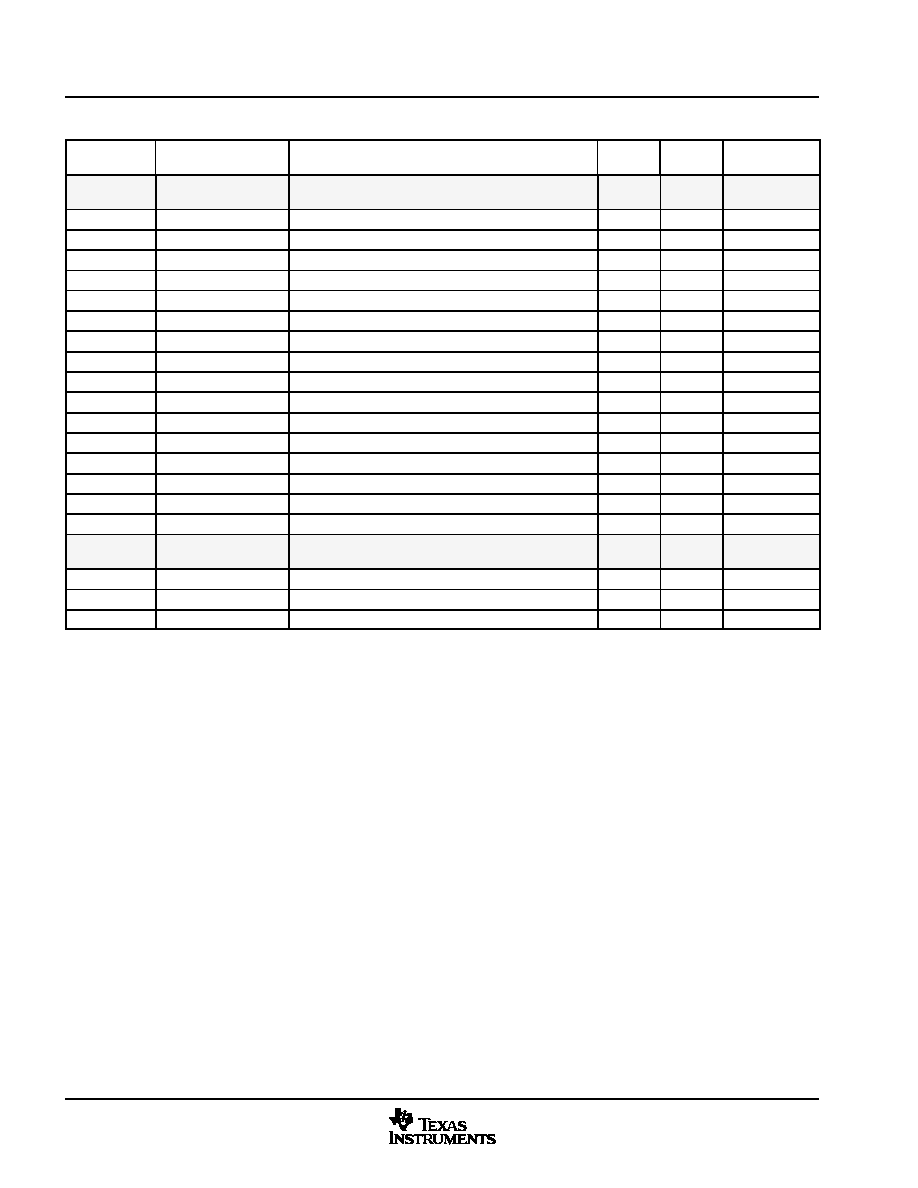
Functional Overview
98
August 2002 - Revised August 2004
SPRS197D
Table 3-52. DSP DMA Controller Registers (Continued)
DSP WORD
ADDRESS
RESET VALUE
ACCESS
TYPE
ACCESS
WIDTH
DESCRIPTION
REGISTER NAME
0x00 0C90h -
0x00 0C9Fh
Reserved
0x00 0CA0h
DMA_CSDP5
Channel 5 Source/Destination Parameters Register
16
RW
0000h
0x00 0CA1h
DMA_CCR5
Channel 5 Control Register
16
RW
0000h
0x00 0CA2h
DMA_CICR5
Channel 5 Interrupt Control Register
16
RW
0003h
0x00 0CA3h
DMA_CSR5
Channel 5 Status Register
16
R
0000h
0x00 0CA4h
DMA_CSSA_L5
Channel 5 Source Start Address Register LSB
16
RW
undef
0x00 0CA5h
DMA_CSSA_U5
Channel 5 Source Start Address Register MSB
16
RW
undef
0x00 0CA6h
DMA_CDSA_L5
Channel 5 Destination Start Address Register LSB
16
RW
undef
0x00 0CA7h
DMA_CDSA_U5
Channel 5 Destination Start Address Register MSB
16
RW
undef
0x00 0CA8h
DMA_CEN5
Channel 5 Element Number Register
16
RW
undef
0x00 0CA9h
DMA_CFN5
Channel 5 Frame Number Register
16
RW
undef
0x00 0CAAh
DMA_CSFI5
Channel 5 Frame Index Register
16
RW
undef
0x00 0CABh
DMA_CSEI5
Channel 5 Element Index Register
16
RW
undef
0x00 0CACh
DMA_CSAC5
Channel 5 Source Address Counter Register
16
RW
undef
0x00 0CADh
DMA_CDAC5
Channel 5 Destination Address Counter Register
16
RW
undef
0x00 0CAEh
DMA_CDFI5
Channel 5 Destination Frame Index
16
RW
undef
0x00 0CAFh
DMA_CDEI5
Channel 5 Destination Element Index
16
RW
undef
0x00 0CB0h -
0x00 0DFFh
Reserved
0x00 0E00h
DMA_GCR
Global Control Register
16
RW
0008h
0x00 0E01h
DMA_GTCR
Global Timeout Control Register
16
RW
0000h
0x00 0E02h
DMA_GSCR
Global Software Incompatible Control Register
16
RW
0000h

Functional Overview
99
August 2002 - Revised August 2004
SPRS197D
Table 3-53. DSP Timer 1 Registers
DSP WORD
ADDRESS
REGISTER NAME
DESCRIPTION
ACCESS
WIDTH
ACCESS
TYPE
RESET
VALUE
0x00 2800h
DSP_CNTL_TIMER_1
DSP Timer 1 Control Timer Register
16
RW
0000h
0x00 2801h
Reserved
0x00 2802h
DSP_LOAD_TIM_HI_1
DSP Timer 1 Load Timer High Register
16
W
undef
0x00 2803h
DSP_LOAD_TIM_LO_1
DSP Timer 1 Load Timer Low Register
16
W
undef
0x00 2804h
DSP_READ_TIM_HI_1
DSP Timer 1 Read Timer High Register
16
R
undef
0x00 2805h
DSP_READ_TIM_LO_1
DSP Timer 1 Read Timer Low Register
16
R
undef
Table 3-54. DSP Timer 2 Registers
DSP WORD
ADDRESS
REGISTER NAME
DESCRIPTION
ACCESS
WIDTH
ACCESS
TYPE
RESET
VALUE
0x00 2C00h
DSP_CNTL_TIMER_2
DSP Timer 2 Control Timer Register
16
RW
0000h
0x00 2C01h
Reserved
0x00 2C02h
DSP_LOAD_TIM_HI_2
DSP Timer 2 Load Timer High Register
16
W
undef
0x00 2C03h
DSP_LOAD_TIM_LO_2
DSP Timer 2 Load Timer Low Register
16
W
undef
0x00 2C04h
DSP_READ_TIM_HI_2
DSP Timer 2 Read Timer High Register
16
R
undef
0x00 2C05h
DSP_READ_TIM_LO_2
DSP Timer 2 Read Timer Low Register
16
R
undef
Table 3-55. DSP Timer 3 Registers
DSP WORD
ADDRESS
REGISTER NAME
DESCRIPTION
ACCESS
WIDTH
ACCESS
TYPE
RESET
VALUE
0x00 3000h
DSP_CNTL_TIMER_3
DSP Timer 3 Control Timer Register
16
RW
0000h
0x00 3001h
Reserved
0x00 3002h
DSP_LOAD_TIM_HI_3
DSP Timer 3 Load Timer High Register
16
W
undef
0x00 3003h
DSP_LOAD_TIM_LO_3
DSP Timer 3 Load Timer Low Register
16
W
undef
0x00 3004h
DSP_READ_TIM_HI_3
DSP Timer 3 Read Timer High Register
16
R
undef
0x00 3005h
DSP_READ_TIM_LO_3
DSP Timer 3 Read Timer Low Register
16
R
undef
Table 3-56. DSP Watchdog Timer Registers
DSP WORD
ADDRESS
REGISTER NAME
DESCRIPTION
ACCESS
WIDTH
ACCESS
TYPE
RESET VALUE
0x00 3400h
DSP_CNTL_TIMER_WD
DSP WDT Control Timer Register
16
RW
0002h
0x00 3401h
Reserved
0x00 3402h
DSP_LOAD_TIM_WD
DSP WDT Load Timer Register
16
W
FFFFh
0x00 3402h
DSP_READ_TIM_WD
DSP WDT Read Timer Register
16
R
FFFFh
0x00 3403h
Reserved
0x00 3404h
DSP_TIMER_MODE_WD
DSP WDT Timer Mode Register
16
RW
8000h
Table 3-57. DSP Interrupt Interface Registers
DSP WORD
ADDRESS
REGISTER NAME
DESCRIPTION
ACCESS
WIDTH
ACCESS
TYPE
RESET
VALUE
0x00 3800h
ET_LS_CTRL_HI
Edge Triggered/Level Sensitive Control Register High
16
RW
0000h
0x00 3801h
ET_LS_CTRL_LO
Edge Triggered/Level Sensitive Control Register Low
16
RW
0000h
0x00 3802h
RST_LVL_LO
Level Sensitive Clear Low Register
16
W
0000h
0x00 3803h
RST_LVL_HI
Level Sensitive Clear High Register
16
W
0000h

Functional Overview
100
August 2002 - Revised August 2004
SPRS197D
Table 3-58. DSP Level 2 Interrupt Handler Registers
DSP WORD
ADDRESS
REGISTER NAME
DESCRIPTION
ACCESS
WIDTH
ACCESS
TYPE
RESET VALUE
0x00 4800h
DSP_L2_ITR
Interrupt Register
16
RW
0000h
0x00 4802h
DSP_L2_MIR
Mask Interrupt Register
16
RW
FFFFh
0x00 4804h
DSP_L2_SIR_IRQ_CODE
IRQ Interrupt Encoded Source Register
16
R
0000h
0x00 4806h
DSP_L2_SIR_FIQ_CODE
FIQ Interrupt Encoded Source Register
16
R
0000h
0x00 4808h
DSP_L2_CONTROL_REG
Interrupt Control Register
16
RW
0000h
0x00 480Ah
DSP_L2_ISR
Software Interrupt Set Register
16
RW
0000h
0x00 480Ch
DSP_L2_ILR0
Interrupt 0 Priority Level Register
16
RW
0000h
0x00 480Eh
DSP_L2_ILR1
Interrupt 1 Priority Level Register
16
RW
0000h
0x00 4810h
DSP_L2_ILR2
Interrupt 2 Priority Level Register
16
RW
0000h
0x00 4812h
DSP_L2_ILR3
Interrupt 3 Priority Level Register
16
RW
0000h
0x00 4814h
DSP_L2_ILR4
Interrupt 4 Priority Level Register
16
RW
0000h
0x00 4816h
DSP_L2_ILR5
Interrupt 5 Priority Level Register
16
RW
0000h
0x00 4818h
DSP_L2_ILR6
Interrupt 6 Priority Level Register
16
RW
0000h
0x00 481Ah
DSP_L2_ILR7
Interrupt 7 Priority Level Register
16
RW
0000h
0x00 481Ch
DSP_L2_ILR8
Interrupt 8 Priority Level Register
16
RW
0000h
0x00 481Eh
DSP_L2_ILR9
Interrupt 9 Priority Level Register
16
RW
0000h
0x00 4820h
DSP_L2_ILR10
Interrupt 10 Priority Level Register
16
RW
0000h
0x00 4822h
DSP_L2_ILR11
Interrupt 11 Priority Level Register
16
RW
0000h
0x00 4824h
DSP_L2_ILR12
Interrupt 12 Priority Level Register
16
RW
0000h
0x00 4826h
DSP_L2_ILR13
Interrupt 13 Priority Level Register
16
RW
0000h
0x00 4828h
DSP_L2_ILR14
Interrupt 14 Priority Level Register
16
RW
0000h
0x00 482Ah
DSP_L2_ILR15
Interrupt 15 Priority Level Register
16
RW
0000h

Functional Overview
101
August 2002 - Revised August 2004
SPRS197D
3.16.2
DSP Public Peripheral Registers
The DSP public peripheral registers include the following:
�
Serial Ports:
-
McBSP1 Registers
-
McBSP3 Registers
-
MCSI1 Registers
-
MCSI2 Registers
Table 3-59. McBSP1 Registers
DSP WORD
ADDRESS
MPU BYTE
ADDRESS
(VIA MPUI)
REGISTER NAME
DESCRIPTION
ACCESS
WIDTH
ACCESS
TYPE
RESET
VALUE
0x00 8C00h
E101:1800
MCBSP1_DRR2
McBSP1 Data Receive Register 2
16
RW
0000h
0x00 8C01h
E101:1802
MCBSP1_DRR1
McBSP1 Data Receive Register 1
16
RW
0000h
0x00 8C02h
E101:1804
MCBSP1_DXR2
McBSP1 Data Transmit Register 2
16
RW
0000h
0x00 8C03h
E101:1806
MCBSP1_DXR1
McBSP1 Data Transmit Register 1
16
RW
0000h
0x00 8C04h
E101:1808
MCBSP1_SPCR2
McBSP1 Serial Port Control Register 2
16
RW
0000h
0x00 8C05h
E101:180A
MCBSP1_SPCR1
McBSP1 Serial Port Control Register 1
16
RW
0000h
0x00 8C06h
E101:180C
MCBSP1_RCR2
McBSP1 Receive Control Register 2
16
RW
0000h
0x00 8C07h
E101:180E
MCBSP1_RCR1
McBSP1 Receive Control Register 1
16
RW
0000h
0x00 8C08h
E101:1810
MCBSP1_XCR2
McBSP1 Transmit Control Register 2
16
RW
0000h
0x00 8C09h
E101:1812
MCBSP1_XCR1
McBSP1 Transmit Control Register 1
16
RW
0000h
0x00 8C0Ah E101:1814
MCBSP1_SRGR2
McBSP1 Sample Rate Generator Register 2
16
RW
2000h
0x00 8C0Bh E101:1816
MCBSP1_SRGR1
McBSP1 Sample Rate Generator Register 1
16
RW
0001h
0x00 8C0Ch E101:1818
MCBSP1_MCR2
McBSP1 Multichannel Control Register 2
16
RW
0000h
0x00 8C0Dh E101:181A
MCBSP1_MCR1
McBSP1 Multichannel Control Register 1
16
RW
0000h
0x00 8C0Eh E101:181C
MCBSP1_RCERA
McBSP1 Receive Channel Enable Register
Partition A
16
RW
0000h
0x00 8C0Fh
E101:181E
MCBSP1_RCERB
McBSP1 Receive Channel Enable Register
Partition B
16
RW
0000h
0x00 8C10h
E101:1820
MCBSP1_XCERA
McBSP1 Transmit Channel Enable Register
Partition A
16
RW
0000h
0x00 8C11h
E101:1822
MCBSP1_XCERB
McBSP1 Transmit Channel Enable Register
Partition B
16
RW
0000h
0x00 8C12h
E101:1824
MCBSP1_PCR0
McBSP1 Pin Control Register 0
16
RW
0000h
0x00 8C13h
E101:1826
MCBSP1_RCERC
McBSP1 Receive Channel Enable Register
Partition C
16
RW
0000h
0x00 8C14h
E101:1828
MCBSP1_RCERD
McBSP1 Receive Channel Enable Register
Partition D
16
RW
0000h
0x00 8C15h
E101:182A
MCBSP1_XCERC
McBSP1 Transmit Channel Enable Register
Partition C
16
RW
0000h
0x00 8C16h
E101:182C
MCBSP1_XCERD
McBSP1 Transmit Channel Enable Register
Partition D
16
RW
0000h
0x00 8C17h
E101:182E
MCBSP1_RCERE
McBSP1 Receive Channel Enable Register
Partition E
16
RW
0000h
0x00 8C18h
E101:1830
MCBSP1_RCERF
McBSP1 Receive Channel Enable Register
Partition F
16
RW
0000h
0x00 8C19h
E101:1832
MCBSP1_XCERE
McBSP1 Transmit Channel Enable Register
Partition E
16
RW
0000h
0x00 8C1Ah E101:1834
MCBSP1_XCERF
McBSP1 Transmit Channel Enable Register
Partition F
16
RW
0000h

Functional Overview
102
August 2002 - Revised August 2004
SPRS197D
Table 3-59. McBSP1 Registers (Continued)
DSP WORD
ADDRESS
RESET
VALUE
ACCESS
TYPE
ACCESS
WIDTH
DESCRIPTION
REGISTER NAME
MPU BYTE
ADDRESS
(VIA MPUI)
0x00 8C1Bh E101:1836
MCBSP1_RCERG
McBSP1 Receive Channel Enable Register
Partition G
16
RW
0000h
0x00 8C1Ch E101:1838
MCBSP1_RCERH
McBSP1 Receive Channel Enable Register
Partition H
16
RW
0000h
0x00 8C1Dh E101:183A
MCBSP1_XCERG
McBSP1 Transmit Channel Enable Register
Partition G
16
RW
0000h
0x00 8C1Eh E101:183C
MCBSP1_XCERH
McBSP1 Transmit Channel Enable Register
Partition H
16
RW
0000h
Table 3-60. McBSP3 Registers
DSP WORD
ADDRESS
MPU BYTE
ADDRESS
(VIA MPUI)
REGISTER NAME
DESCRIPTION
ACCESS
WIDTH
ACCESS
TYPE
RESET
VALUE
0x00 B800h E101:7000
MCBSP3_DRR2
McBSP3 Data Receive Register 2
16
RW
0000h
0x00 B801h E101:7002
MCBSP3_DRR1
McBSP3 Data Receive Register 1
16
RW
0000h
0x00 B802h E101:7004
MCBSP3_DXR2
McBSP3 Data Transmit Register 2
16
RW
0000h
0x00 B803h E101:7006
MCBSP3_DXR1
McBSP3 Data Transmit Register 1
16
RW
0000h
0x00 B804h E101:7008
MCBSP3_SPCR2
McBSP3 Serial Port Control Register 2
16
RW
0000h
0x00 B805h E101:700A
MCBSP3_SPCR1
McBSP3 Serial Port Control Register 1
16
RW
0000h
0x00 B806h E101:700C
MCBSP3_RCR2
McBSP3 Receive Control Register 2
16
RW
0000h
0x00 B807h E101:700E
MCBSP3_RCR1
McBSP3 Receive Control Register 1
16
RW
0000h
0x00 B808h E101:7010
MCBSP3_XCR2
McBSP3 Transmit Control Register 2
16
RW
0000h
0x00 B809h E101:7012
MCBSP3_XCR1
McBSP3 Transmit Control Register 1
16
RW
0000h
0x00 B80Ah E101:7014
MCBSP3_SRGR2
McBSP3 Sample Rate Generator Register 2
16
RW
2000h
0x00 B80Bh E101:7016
MCBSP3_SRGR1
McBSP3 Sample Rate Generator Register 1
16
RW
0001h
0x00 B80Ch E101:7018
MCBSP3_MCR2
McBSP3 Multichannel Control Register 2
16
RW
0000h
0x00 B80Dh E101:701A
MCBSP3_MCR1
McBSP3 Multichannel Control Register 1
16
RW
0000h
0x00 B80Eh E101:701C
MCBSP3_RCERA
McBSP3 Receive Channel Enable Register
Partition A
16
RW
0000h
0x00 B80Fh E101:701E
MCBSP3_RCERB
McBSP3 Receive Channel Enable Register
Partition B
16
RW
0000h
0x00 B810h E101:7020
MCBSP3_XCERA
McBSP3 Transmit Channel Enable Register
Partition A
16
RW
0000h
0x00 B811h E101:7022
MCBSP3_XCERB
McBSP3 Transmit Channel Enable Register
Partition B
16
RW
0000h
0x00 B812h E101:7024
MCBSP3_PCR0
McBSP3 Pin Control Register 0
16
RW
0000h
0x00 B813h E101:7026
MCBSP3_RCERC
McBSP3 Receive Channel Enable Register
Partition C
16
RW
0000h
0x00 B814h E101:7028
MCBSP3_RCERD
McBSP3 Receive Channel Enable Register
Partition D
16
RW
0000h
0x00 B815h E101:702A
MCBSP3_XCERC
McBSP3 Transmit Channel Enable Register
Partition C
16
RW
0000h
0x00 B816h E101:702C
MCBSP3_XCERD
McBSP3 Transmit Channel Enable Register
Partition D
16
RW
0000h
0x00 B817h E101:702E
MCBSP3_RCERE
McBSP3 Receive Channel Enable Register
Partition E
16
RW
0000h
0x00 B818h E101:7030
MCBSP3_RCERF
McBSP3 Receive Channel Enable Register
Partition F
16
RW
0000h

Functional Overview
103
August 2002 - Revised August 2004
SPRS197D
Table 3-60. McBSP3 Registers (Continued)
DSP WORD
ADDRESS
RESET
VALUE
ACCESS
TYPE
ACCESS
WIDTH
DESCRIPTION
REGISTER NAME
MPU BYTE
ADDRESS
(VIA MPUI)
0x00 B819h E101:7032
MCBSP3_XCERE
McBSP3 Transmit Channel Enable Register
Partition E
16
RW
0000h
0x00 B81Ah E101:7034
MCBSP3_XCERF
McBSP3 Transmit Channel Enable Register
Partition F
16
RW
0000h
0x00 B81Bh E101:7036
MCBSP3_RCERG
McBSP3 Receive Channel Enable Register
Partition G
16
RW
0000h
0x00 B81Ch E101:7038
MCBSP3_RCERH
McBSP3 Receive Channel Enable Register
Partition H
16
RW
0000h
0x00 B81Dh E101:703A
MCBSP3_XCERG
McBSP3 Transmit Channel Enable Register
Partition G
16
RW
0000h
0x00 B81Eh E101:703C
MCBSP3_XCERH
McBSP3 Transmit Channel Enable Register
Partition H
16
RW
0000h

Functional Overview
104
August 2002 - Revised August 2004
SPRS197D
Table 3-61. MCSI1 Registers
DSP WORD
ADDRESS
MPU BYTE
ADDRESS
(VIA MPUI)
REGISTER NAME
DESCRIPTION
ACCESS
WIDTH
ACCESS
TYPE
RESET
VALUE
0x00 9400h
E101:2800
MCSI1_CONTROL_REG
MCSI1 Control Register
16
RW
0000h
0x00 9401h
E101:2802
MCSI1_MAIN_PARAMETERS_REG MCSI1 Main Parameters Register
16
RW
0000h
0x00 9402h
E101:2804
MCSI1_INTERRUPTS_REG
MCSI1 Interrupts Register
16
RW
0000h
0x00 9403h
E101:2806
MCSI1_CHANNEL_USED_REG
MCSI1 Channel Used Register
16
RW
0000h
0x00 9404h
E101:2808
MCSI1_OVER_CLOCK_REG
MCSI1 Over-Clock Register
16
RW
0000h
0x00 9405h
E101:280A MCSI1_CLOCK_FREQUENCY_
REG
MCSI1 Clock Frequency Register
16
RW
0000h
0x00 9406h
E101:280C MCSI1_STATUS_REG
MCSI1 Status Register
16
RW
0000h
0x00 9407h-
0x00 941Fh
Reserved
0x00 9420h
E101:2840
MCSI1_TX0
MCSI1 Transmit Word Register 0
16
RW
Undefined
0x00 9421h
E101:2842
MCSI1_TX1
MCSI1 Transmit Word Register 1
16
RW
Undefined
0x00 9422h
E101:2844
MCSI1_TX2
MCSI1 Transmit Word Register 2
16
RW
Undefined
0x00 9423h
E101:2846
MCSI1_TX3
MCSI1 Transmit Word Register 3
16
RW
Undefined
0x00 9424h
E101:2848
MCSI1_TX4
MCSI1 Transmit Word Register 4
16
RW
Undefined
0x00 9425h
E101:284A MCSI1_TX5
MCSI1 Transmit Word Register 5
16
RW
Undefined
0x00 9426h
E101:284C MCSI1_TX6
MCSI1 Transmit Word Register 6
16
RW
Undefined
0x00 9427h
E101:284E MCSI1_TX7
MCSI1 Transmit Word Register 7
16
RW
Undefined
0x00 9428h
E101:2850
MCSI1_TX8
MCSI1 Transmit Word Register 8
16
RW
Undefined
0x00 9429h
E101:2852
MCSI1_TX9
MCSI1 Transmit Word Register 9
16
RW
Undefined
0x00 942Ah
E101:2854
MCSI1_TX10
MCSI1 Transmit Word Register 10
16
RW
Undefined
0x00 942Bh
E101:2856
MCSI1_TX11
MCSI1 Transmit Word Register 11
16
RW
Undefined
0x00 942Ch
E101:2858
MCSI1_TX12
MCSI1 Transmit Word Register 12
16
RW
Undefined
0x00 942Dh
E101:285A MCSI1_TX13
MCSI1 Transmit Word Register 13
16
RW
Undefined
0x00 942Eh
E101:285C MCSI1_TX14
MCSI1 Transmit Word Register 14
16
RW
Undefined
0x00 942Fh
E101:285E MCSI1_TX15
MCSI1 Transmit Word Register 15
16
RW
Undefined
0x00 9430h
E101:2860
MCSI1_RX0
MCSI1 Receive Word Register 0
16
R
Undefined
0x00 9431h
E101:2862
MCSI1_RX1
MCSI1 Receive Word Register 1
16
R
Undefined
0x00 9432h
E101:2864
MCSI1_RX2
MCSI1 Receive Word Register 2
16
R
Undefined
0x00 9433h
E101:2866
MCSI1_RX3
MCSI1 Receive Word Register 3
16
R
Undefined
0x00 9434h
E101:2868
MCSI1_RX4
MCSI1 Receive Word Register 4
16
R
Undefined
0x00 9435h
E101:286A MCSI1_RX5
MCSI1 Receive Word Register 5
16
R
Undefined
0x00 9436h
E101:286C MCSI1_RX6
MCSI1 Receive Word Register 6
16
R
Undefined
0x00 9437h
E101:286E MCSI1_RX7
MCSI1 Receive Word Register 7
16
R
Undefined
0x00 9438h
E101:2870
MCSI1_RX8
MCSI1 Receive Word Register 8
16
R
Undefined
0x00 9439h
E101:2872
MCSI1_RX9
MCSI1 Receive Word Register 9
16
R
Undefined
0x00 943Ah
E101:2874
MCSI1_RX10
MCSI1 Receive Word Register 10
16
R
Undefined
0x00 943Bh
E101:2876
MCSI1_RX11
MCSI1 Receive Word Register 11
16
R
Undefined
0x00 943Ch
E101:2878
MCSI1_RX12
MCSI1 Receive Word Register 12
16
R
Undefined
0x00 943Dh
E101:287A MCSI1_RX13
MCSI1 Receive Word Register 13
16
R
Undefined
0x00 943Eh
E101:287C MCSI1_RX14
MCSI1 Receive Word Register 14
16
R
Undefined
0x00 943Fh
E101:287E MCSI1_RX15
MCSI1 Receive Word Register 15
16
R
Undefined
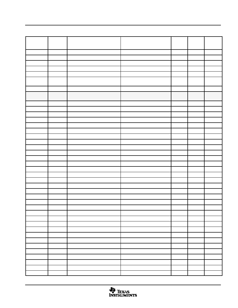
Functional Overview
105
August 2002 - Revised August 2004
SPRS197D
Table 3-62. MCSI2 Registers
DSP WORD
ADDRESS
MPU BYTE
ADDRESS
(VIA MPUI)
REGISTER NAME
DESCRIPTION
ACCESS
WIDTH
ACCESS
TYPE
RESET
VALUE
0x00 9000h
E101:2000
MCSI2_CONTROL_REG
MCSI2 control register
16
RW
0000h
0x00 9001h
E101:2002
MCSI2_MAIN_PARAMETERS_REG MCSI2 main parameters register
16
RW
0000h
0x00 9002h
E101:2004
MCSI2_INTERRUPTS_REG
MCSI2 interrupts register
16
RW
0000h
0x00 9003h
E101:2006
MCSI2_CHANNEL_USED_REG
MCSI2 channel used register
16
RW
0000h
0x00 9004h
E101:2008
MCSI2_OVER_CLOCK_REG
MCSI2 over-clock register
16
RW
0000h
0x00 9005h
E101:200A MCSI2_CLOCK_FREQUENCY_
REG
MCSI2 clock frequency register
16
RW
0000h
0x00 9006h
E101:200C MCSI2_STATUS_REG
MCSI2 status register
16
RW
0000h
0x00 9007h -
0x00 901Fh
Reserved
0x00 9020h
E101:2040
MCSI2_TX0
MCSI2 Transmit Word Register 0
16
RW
Undefined
0x00 9021h
E101:2042
MCSI2_TX1
MCSI2 Transmit Word Register 1
16
RW
Undefined
0x00 9022h
E101:2044
MCSI2_TX2
MCSI2 Transmit Word Register 2
16
RW
Undefined
0x00 9023h
E101:2046
MCSI2_TX3
MCSI2 Transmit Word Register 3
16
RW
Undefined
0x00 9024h
E101:2048
MCSI2_TX4
MCSI2 Transmit Word Register 4
16
RW
Undefined
0x00 9025h
E101:204A MCSI2_TX5
MCSI2 Transmit Word Register 5
16
RW
Undefined
0x00 9026h
E101:204C MCSI2_TX6
MCSI2 Transmit Word Register 6
16
RW
Undefined
0x00 9027h
E101:204E MCSI2_TX7
MCSI2 Transmit Word Register 7
16
RW
Undefined
0x00 9028h
E101:2050
MCSI2_TX8
MCSI2 Transmit Word Register 8
16
RW
Undefined
0x00 9029h
E101:2052
MCSI2_TX9
MCSI2 Transmit Word Register 9
16
RW
Undefined
0x00 902Ah
E101:2054
MCSI2_TX10
MCSI2 Transmit Word Register 10
16
RW
Undefined
0x00 902Bh
E101:2056
MCSI2_TX11
MCSI2 Transmit Word Register 11
16
RW
Undefined
0x00 902Ch
E101:2058
MCSI2_TX12
MCSI2 Transmit Word Register 12
16
RW
Undefined
0x00 902Dh
E101:205A MCSI2_TX13
MCSI2 Transmit Word Register 13
16
RW
Undefined
0x00 902Eh
E101:205C MCSI2_TX14
MCSI2 Transmit Word Register 14
16
RW
Undefined
0x00 902Fh
E101:205E MCSI2_TX15
MCSI2 Transmit Word Register 15
16
RW
Undefined
0x00 9030h
E101:2060
MCSI2_RX0
MCSI2 Receive Word Register 0
16
R
Undefined
0x00 9031h
E101:2062
MCSI2_RX1
MCSI2 Receive Word Register 1
16
R
Undefined
0x00 9032h
E101:2064
MCSI2_RX2
MCSI2 Receive Word Register 2
16
R
Undefined
0x00 9033h
E101:2066
MCSI2_RX3
MCSI2 Receive Word Register 3
16
R
Undefined
0x00 9034h
E101:2068
MCSI2_RX4
MCSI2 Receive Word Register 4
16
R
Undefined
0x00 9035h
E101:206A MCSI2_RX5
MCSI2 Receive Word Register 5
16
R
Undefined
0x00 9036h
E101:206C MCSI2_RX6
MCSI2 Receive Word Register 6
16
R
Undefined
0x00 9037h
E101:206E MCSI2_RX7
MCSI2 Receive Word Register 7
16
R
Undefined
0x00 9038h
E101:2070
MCSI2_RX8
MCSI2 Receive Word Register 8
16
R
Undefined
0x00 9039h
E101:2072
MCSI2_RX9
MCSI2 Receive Word Register 9
16
R
Undefined
0x00 903Ah
E101:2074
MCSI2_RX10
MCSI2 Receive Word Register 10
16
R
Undefined
0x00 903Bh
E101:2076
MCSI2_RX11
MCSI2 Receive Word Register 11
16
R
Undefined
0x00 903Ch
E101:2078
MCSI2_RX12
MCSI2 Receive Word Register 12
16
R
Undefined
0x00 903Dh
E101:207A MCSI2_RX13
MCSI2 Receive Word Register 13
16
R
Undefined
0x00 903Eh
E101:207C MCSI2_RX14
MCSI2 Receive Word Register 14
16
R
Undefined
0x00 903Fh
E101:207E MCSI2_RX15
MCSI2 Receive Word Register 15
16
R
Undefined
Functional Overview
106
August 2002 - Revised August 2004
SPRS197D
3.16.3
DSP Configuration Registers
The DSP configuration registers include the following:
�
I-Cache and EMIF setup
-
DSP Instruction Cache Registers
-
DSP EMIF Configuration Registers
�
TIPB setup
-
DSP TIPB Bridge Configuration Registers
-
DSP UART TI Peripheral Bus Switch Registers
�
Clock Control:
-
DSP Clock Mode Registers
Table 3-63. DSP Instruction Cache Registers
DSP WORD
ADDRESS
REGISTER NAME
DESCRIPTION
ACCESS
WIDTH
ACCESS
TYPE
RESET
VALUE
0x00 1400h
ICGC
I-Cache Global Control Register
16
RW
C006h
0x00 1401h
Reserved
16
RW
0000h
0x00 1402h
Reserved
16
RW
0000h
0x00 1403h
ICWC
I-Cache Way Control Register
16
RW
000Dh
0x00 1404h
ICST
I-Cache Status Register
16
R
0000h
0x00 1405h
ICRC1
I-Cache Ramset 1 Control Register
16
RW
000Dh
0x00 1406h
ICRTAG1
I-Cache Remset 1 TAG Register
16
RW
0000h
0x00 1407h
ICRC2
I-Cache Ramset 2 Control Register
16
RW
000Dh
0x00 1408h
ICRTAG2
I-Cache Remset 2 TAG Register
16
RW
0000h
Table 3-64. DSP EMIF Configuration Register
DSP WORD
ADDRESS
REGISTER NAME
DESCRIPTION
ACCESS
WIDTH
ACCESS
TYPE
RESET
VALUE
0x00 0800h
DSP_EMIF_GCR
DSP EMIF Global Control Register
16
RW
0020h
0x00 0801h
DSP_EMIF_GRR
DSP EMIF Global Reset Register
16
RW
undef
Table 3-65. DSP TIPB Bridge Configuration Registers
DSP WORD
ADDRESS
REGISTER NAME
DESCRIPTION
ACCESS
WIDTH
ACCESS
TYPE
RESET
VALUE
0x00 0000h
TIPB_CMR
DSP TIPB Bridge Control Mode Register
16
RW
FE4Dh
0x00 0001h
TIPB_ICR
DSP TIPB Bridge Idle Control Register
16
RW
0000h
0x00 0002h
TIPB_ISTR
DSP TIPB Bridge Idle Status Register
16
R
0000h

Functional Overview
107
August 2002 - Revised August 2004
SPRS197D
Table 3-66. DSP UART TIPB Bus Switch Registers
DSP WORD
ADDRESS
REGISTER NAME
DESCRIPTION
ACCESS
WIDTH
ACCESS
TYPE
RESET
VALUE
0x00 E400h
RHSW_DSP_CNF1
UART1 TIPB Switch Configuration Register (DSP)
16
RW
0001h
0x00 E402h
RHSW_DSP_STA1
UART1 TIPB Switch Status Register (DSP)
16
R
0001h
0x00 E404-
0x00 E0Eh
Reserved
0x00 E410h
RHSW_DSP_CNF2
UART2 TIPB Switch Configuration Register (DSP)
16
RW
0001h
0x00 E412h
RHSW_DSP_STA2
UART2 TIPB Switch Status Register (DSP)
16
R
0001h
0x00 E414-
0x00 E1Eh
Reserved
0x00 E420h
RHSW_DSP_CNF3
UART3 TIPB Switch Configuration Register (DSP)
16
RW
0001h
0x00 E422h
RHSW_DSP_STA3
UART3 TIPB Switch Status Register (DSP)
16
R
0001h
Table 3-67. DSP Clock Mode Registers
DSP WORD
ADDRESS
MPU BYTE
ADDRESS
(VIA MPUI)
REGISTER NAME
DESCRIPTION
ACCESS
WIDTH
ACCESS
TYPE
RESET
VALUE
0x00 4000h
E100:8000
DSP_CKCTL
DSP Clock Control Register
16
RW
0000h
0x00 4002h
E100:8004
DSP_IDLECT1
DSP Idle Control 1 Register
16
RW
0000h
0x00 4004h
E100:8008
DSP_IDLECT2
DSP Idle Control 2 Register
16
RW
0000h
0x00 4006h -
0x00 4008h
Reserved
0x00 400Ah
E100:8014
DSP_RSTCT2
DSP Peripheral Reset Control Register
16
RW
0000h
0x00 400Ch
E100:8018
DSP_SYSST
DSP System Status Register
16
RW
0000h

Functional Overview
108
August 2002 - Revised August 2004
SPRS197D
3.16.4
MPU/DSP Shared Peripheral Register Descriptions
The following tables describe the MPU/DSP shared peripheral registers including register addresses,
descriptions, required access widths, access types (R-read, W-write, RW-read/write) and reset values. These
tables are organized by function with like peripherals or functions together and are therefore not necessarily
in order of ascending register addresses. Reserved addresses should never be accessed.
NOTE: All accesses to these registers must be of the data access widths indicated to avoid
a TIPB bus error condition and a corresponding interrupt. Reserved addresses should never
be accessed.
The MPU/DSP shared peripheral registers include the following:
�
UARTs:
-
UART1 Registers
-
UART2 Registers
-
UART3/IrDA Registers
�
GPIO and Mailboxes
-
MPU/DSP Shared GPIO Registers
-
MPU/DSP Shared Mailbox Registers
Functional Overview
109
August 2002 - Revised August 2004
SPRS197D
Table 3-68. UART1 Registers
DSP WORD
ADDRESS
MPU BYTE
ADDRESS
MPU BYTE
ADDRESS
(VIA MPUI)
REGISTER
NAME
DESCRIPTION
ACCESS
WIDTH
ACCESS
TYPE
RESET
VALUE
0x00 8000h
FFFB:0000
E101:0000
UART1_RHR
UART1 Receive Holding Register
8
R
Undefined
0x00 8000h
FFFB:0000
E101:0000
UART1_THR
UART1 Transmit Holding Register
8
W
Undefined
0x00 8000h
FFFB:0000
E101:0000
UART1_DLL
�
UART1 Divisor Latch Low Register
8
RW
00h
0x00 8001h
FFFB:0004
E101:0002
UART1_IER
UART1 Interrupt Enable Register
8
RW
00h
0x00 8001h
FFFB:0004
E101:0002
UART1_DLH
�
UART1 Divisor Latch High Register
8
RW
00h
0x00 8002h
FFFB:0008
E101:0004
UART1_IIR
UART1 Interrupt Identification
Register
8
R
01h
0x00 8002h
FFFB:0008
E101:0004
UART1_FCR
�
UART1 FIFO Control Register
8
W
00h
0x00 8002h
FFFB:0008
E101:0004
UART1_EFR
�
UART1 Enhanced Feature Register
8
RW
00h
0x00 8003h
FFFB:000C
E101:0006
UART1_LCR
UART1 Line Control Register
8
RW
00h
0x00 8004h
FFFB:0010
E101:0008
UART1_MCR
�
UART1 Modem Control Register
8
RW
00h
0x00 8004h
FFFB:0010
E101:0008
UART1_XON1
�
UART1 XON1 Register
8
RW
00h
0x00 8005h
FFFB:0014
E101:000A
UART1_LSR
UART1 Mode Register
8
R
60h
0x00 8005h
FFFB:0014
E101:000A
UART1_XON2
�
UART1 XON2 Register
8
RW
00h
0x00 8006h
FFFB:0018
E101:000C
UART1_MSR
UART1 Modem Status Register
8
R
Undefined
0x00 8006h
FFFB:0018
E101:000C
UART1_TCR
#
UART1 Transmission
Control Register
8
RW
0Fh
0x00 8006h
FFFB:0018
E101:000C
UART1_XOFF1
�
UART1 XOFF1 Register
8
RW
00h
0x00 8007h
FFFB:001C
E101:000E
UART1_SPR
UART1 Scratchpad Register
8
RW
00h
0x00 8007h
FFFB:001C
E101:000E
UART1_TLR
#
UART1 Trigger Level Register
8
RW
00h
0x00 8007h
FFFB:001C
E101:000E
UART1_XOFF2
�
UART1 XOFF2 Register
8
RW
00h
0x00 8008h
FFFB:0020
E101:0010
UART1_MDR1
UART1 Mode Definition 1 Register
8
RW
07h
0x00 8009h -
0x00 800Dh
FFFB:0024 -
FFFB:0034
Reserved
0x00 800Eh
FFFB:0038
E101:001C
UART1_UASR
�
UART1 Autobauding Status
Register
8
R
00h
0x00 800Fh
FFFB:003C
Reserved
0x00 8010h
FFFB:0040
E101:0020
UART1_SCR
UART1 Supplementary Control
Register
8
RW
00h
0x00 8011h
FFFB:0044
E101:0022
UART1_SSR
UART1 Supplementary Status
Register
8
R
00h
0x00 8012h
FFFB:0048
Reserved
0x00 8013h
FFFB:004C
E101:0026
UART1_OSC_
12M_SEL
UART1 12-/13-MHz Oscillator
Select Register
8
W
00h
0x00 8014h
FFFB:0050
E101:0028
UART1_MVR
UART1 Module Version Register
8
R
-
Register is accessible when LCR[7] = 0 (normal operating mode)
Register is accessible when LCR[7] = 1 and LCR[7:0] 0BFh
�
Register is accessible when LCR[7] = 0BFh
�
Register is write accessible when EFR[4] = 1
#
Register is accessible when EFR[4] = 1 and MCR[6] = 1

Functional Overview
110
August 2002 - Revised August 2004
SPRS197D
Table 3-69. UART2 Registers
DSP WORD
ADDRESS
MPU BYTE
ADDRESS
MPU BYTE
ADDRESS
(VIA MPUI)
REGISTER
NAME
DESCRIPTION
ACCESS
WIDTH
ACCESS
TYPE
RESET
VALUE
0x00 8400h
FFFB:0800
E101:0800
UART2_RHR
UART2 Receive Holding Register
8
R
Undefined
0x00 8400h
FFFB:0800
E101:0800
UART2_THR
UART2 Transmit Holding Register
8
W
Undefined
0x00 8400h
FFFB:0800
E101:0800
UART2_DLL
�
UART2 Divisor Latch Low Register
8
RW
00h
0x00 8401h
FFFB:0804
E101:0802
UART2_IER
UART2 Interrupt Enable Register
8
RW
00h
0x00 8401h
FFFB:0804
E101:0802
UART2_DLH
�
UART2 Divisor Latch High Register
8
RW
00h
0x00 8402h
FFFB:0808
E101:0804
UART2_IIR
UART2 Interrupt Identification
Register
8
R
01h
0x00 8402h
FFFB:0808
E101:0804
UART2_FCR
�
UART2 FIFO Control Register
8
W
00h
0x00 8402h
FFFB:0808
E101:0804
UART2_EFR
�
UART2 Enhanced Feature Register
8
RW
00h
0x00 8403h
FFFB:080C
E101:0806
UART2_LCR
UART2 Line Control Register
8
RW
00h
0x00 8404h
FFFB:0810
E101:0808
UART2_MCR
�
UART2 Modem Control Register
8
RW
00h
0x00 8404h
FFFB:0810
E101:0808
UART2_XON1
�
UART2 XON1 Register
8
RW
00h
0x00 8405h
FFFB:0814
E101:080A
UART2_LSR
UART2 Mode Register
8
R
60h
0x00 8405h
FFFB:0814
E101:080A
UART2_XON2
�
UART2 XON2 Register
8
RW
00h
0x00 8406h
FFFB:0818
E101:080C
UART2_MSR
UART2 Modem Status Register
8
R
Undefined
0x00 8406h
FFFB:0818
E101:080C
UART2_TCR
#
UART2 Transmission Control
Register
8
RW
0Fh
0x00 8406h
FFFB:0818
E101:080C
UART2_XOFF1
�
UART2 XOFF1 Register
8
RW
00h
0x00 8407h
FFFB:081C
E101:080E
UART2_SPR
UART2 Scratchpad Register
8
RW
00h
0x00 8407h
FFFB:081C
E101:080E
UART2_TLR
#
UART2 Trigger Level Register
8
RW
00h
0x00 8407h
FFFB:081C
E101:080E
UART2_XOFF2
�
UART2 XOFF2 Register
8
RW
00h
0x00 8408h
FFFB:0820
E101:0810
UART2_MDR1
UART2 Mode Definition 1 Register
8
RW
07h
0x00 8409 -
0x00840Dh
FFFB:0824 -
FFFB:0834
Reserved
0x00 840Eh FFFB:0838
E101:081C
UART2_UASR
�
UART2 Autobauding Status Register
8
R
00h
0x00 840Fh
FFFB:083C
Reserved
0x00 8410h
FFFB:0840
E101:0820
UART2_SCR
UART2 Supplementary Control
Register
8
RW
00h
0x00 8411h
FFFB:0844
E101:0822
UART2_SSR
UART2 Supplementary Status
Register
8
R
00h
0x00 8412h
FFFB:0848
Reserved
0x00 8413h
FFFB:084C
E101:0826
UART2_OSC_
12M_SELV
UART2 12-/13-MHz Oscillator Select
Register
8
W
00h
0x00 8414h
FFFB:0850
E101:0828
UART2_MVR
UART2 Module Version Register
8
R
-
Register is accessible when LCR[7] = 0 (normal operating mode)
Register is accessible when LCR[7] = 1 and LCR[7:0] 0BFh
�
Register is accessible when LCR[7] = 0BFh
�
Register is write accessible when EFR[4] = 1
#
Register is accessible when EFR[4] = 1 and MCR[6] = 1
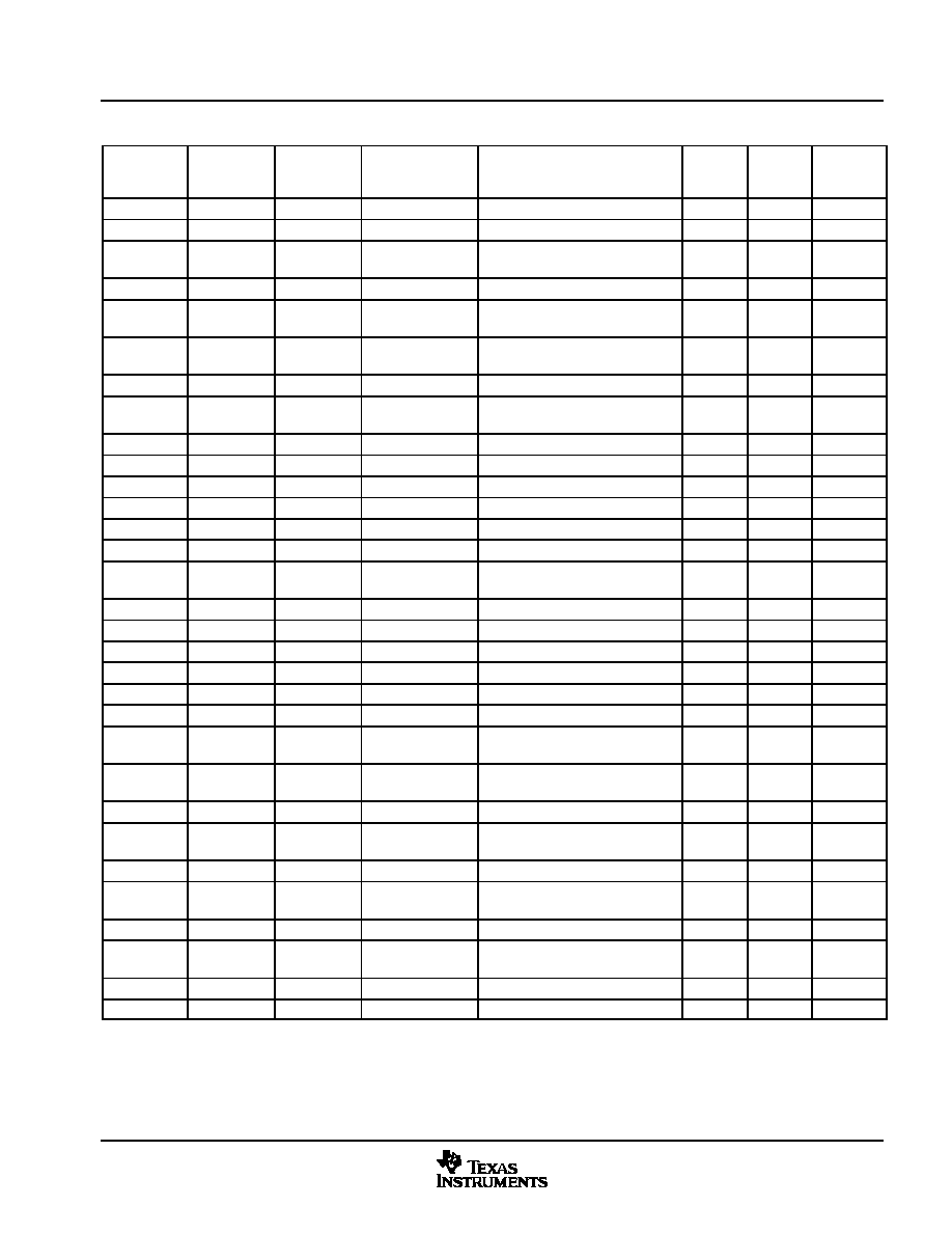
Functional Overview
111
August 2002 - Revised August 2004
SPRS197D
Table 3-70. UART3/IrDA Registers
DSP WORD
ADDRESS
MPU BYTE
ADDRESS
MPU BYTE
ADDRESS
(VIA MPUI)
REGISTER
NAME
DESCRIPTION
ACCESS
WIDTH
ACCESS
TYPE
RESET
VALUE
0x00 CC00h
FFFB:9800
E101:9800
UART3_RHR
UART3 Receive Holding Register
8
R
Undefined
0x00 CC00h
FFFB:9800
E101:9800
UART3_THR
UART3 Transmit Holding Register
8
W
Undefined
0x00 CC00h
FFFB:9800
E101:9800
UART3_DLL
�
UART3 Divisor Latch Low
Register
8
RW
00h
0x00 CC01h
FFFB:9804
E101:9802
UART3_IER
UART3 Interrupt Enable Register
8
RW
00h
0x00 CC01h
FFFB:9804
E101:9802
UART3_DLH
�
UART3 Divisor Latch High
Register
8
RW
00h
0x00 CC02h
FFFB:9808
E101:9804
UART3_IIR
UART3 Interrupt Identification
Register
8
R
01h
0x00 CC02h
FFFB:9808
E101:9804
UART3_FCR
�
UART3 FIFO Control Register
8
W
00h
0x00 CC02h
FFFB:9808
E101:9804
UART3_EFR
�
UART3 Enhanced Feature
Register
8
RW
00h
0x00 CC03h
FFFB:980C
E101:9806
UART3_LCR
UART3 Line Control Register
8
RW
00h
0x00 CC04h
FFFB:9810
E101:9808
UART3_MCR
�
UART3 Modem Control Register
8
RW
00h
0x00 CC04h
FFFB:9810
E101:9808
UART3_XON1
�
UART3 XON1 Register
8
RW
00h
0x00 CC05h
FFFB:9814
E101:980A
UART3_LSR
UART3 Mode Register
8
R
60h
0x00 CC05h
FFFB:9814
E101:980A
UART3_XON2
�
UART3 XON2 Register
8
RW
00h
0x00 CC06h
FFFB:9818
E101:980C
UART3_MSR
UART3 Modem Status Register
8
R
Undefined
0x00 CC06h
FFFB:9818
E101:980C
UART3_TCR
#
UART3 Transmission Control
Register
8
RW
0Fh
0x00 CC06h
FFFB:9818
E101:980C
UART3_XOFF1
�
UART3 XOFF1 Register
8
RW
00h
0x00 CC07h
FFFB:981C
E101:980E
UART3_SPR
UART3 Scratchpad Register
8
RW
00h
0x00 CC07h
FFFB:981C
E101:980E
UART3_TLR
#
UART3 Trigger Level Register
8
RW
00h
0x00 CC07h
FFFB:981C
E101:980E
UART3_XOFF2
�
UART3 XOFF2 Register
8
RW
00h
0x00 CC08h
FFFB:9820
E101:9810
UART3_MDR1
UART3 Mode Definition 1 Register
8
RW
07h
0x00 CC09h
FFFB:9824
E101:9812
UART3_MDR2
UART3 Mode Definition Register 2
8
RW
00h
0x00 CC0Ah FFFB:9828
E101:9814
UART3_SFLSR
UART3 Status FIFO Line Status
Register
8
R
00h
0x00 CC0Ah FFFB:9828
E101:9814
UART3_TXFLL
UART3 Transmit Frame Length
Low
8
W
00h
0x00 CC0Bh FFFB:982C
E101:9816
UART3_RESUME
UART3 Resume Register
8
R
00h
0x00 CC0Bh FFFB:982C
E101:9816
UART3_TXFLH
UART3 Transmit Frame Length
High
8
W
00h
0x00 CC0Ch FFFB:9830
E101:9818
UART3_SFREGL
UART3 Status FIFO Low Register
8
R
Undefined
0x00 CC0Ch FFFB:9830
E101:9818
UART3_RXFLL
UART3 Receive Frame Length
Low
8
W
00h
0x00 CC0Dh FFFB:9834
E101:981A
UART3_SFREGH
UART3 Status FIFO High Register
8
R
Undefined
0x00 CC0Dh FFFB:9834
E101:981A
UART3_RXFLH
UART3 Receive Frame Length
High
8
W
00h
0x00 CC0Eh FFFB:9838
E101:981C
UART3_BLR
UART3 BOF Control Register
8
RW
40h
0x00 CC0Fh
FFFB:983C
E101:981E
UART3_ACREG
UART3 Auxiliary Control Register
8
RW
00h
Register is accessible when LCR[7] = 0 (normal operating mode)
Register is accessible when LCR[7] = 1 and LCR[7:0] 0BFh
�
Register is accessible when LCR[7] = 0BFh
�
Register is write accessible when EFR[4] = 1
#
Register is accessible when EFR[4] = 1 and MCR[6] = 1
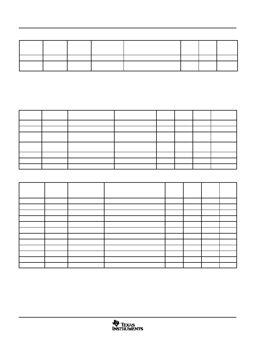
Functional Overview
112
August 2002 - Revised August 2004
SPRS197D
Table 3-70. UART3/IrDA Registers (Continued)
DSP WORD
ADDRESS
RESET
VALUE
ACCESS
TYPE
ACCESS
WIDTH
DESCRIPTION
REGISTER
NAME
MPU BYTE
ADDRESS
(VIA MPUI)
MPU BYTE
ADDRESS
0x00 CC0Fh
FFFB:983C
E101:981E
UART3_DIV16
�
UART3 Divide 1.6 Register
8
RW
00h
0x00 CC10h
FFFB:9840
E101:9820
UART3_SCR
UART3 Supplementary Control
Register
8
RW
00h
Register is accessible when LCR[7] = 0 (normal operating mode)
Register is accessible when LCR[7] = 1 and LCR[7:0] 0BFh
�
Register is accessible when LCR[7] = 0BFh
�
Register is write accessible when EFR[4] = 1
#
Register is accessible when EFR[4] = 1 and MCR[6] = 1
Table 3-71. MPU/DSP Shared GPIO Registers
DSP WORD
ADDRESS
MPU BYTE
ADDRESS
REGISTER NAME
DESCRIPTION
ACCESS
WIDTH
MPU
ACCESS
DSP
ACCESS
RESET
VALUE
0x00 F000h
FFFC:E000
DATA_INPUT
Data Input Register
16
R
R
0000h
0x00 F002h
FFFC:E004
DATA_OUTPUT
Data Output Register
16
RW
RW
FFFFh
0x00 F004h
FFFC:E008
DIRECTION_CONTROL
Direction Control
Register
16
RW
RW
FFFFh
0x00 F006h
FFFC:E00C
INTERRUPT_CONTROL
Interrupt Control
Register
16
RW
RW
FFFFh
0x00 F008h
FFFC:E010
INTERRUPT_MASK
Interrupt Mask Register
16
RW
RW
FFFFh
0x00 F00Ah FFFC:E014
INTERRUPT_STATUS
Interrupt Status Register
16
RW
RW
0000h
0x00 F00Ch FFFC:E018
PIN_CONTROL
Pin Control Register
16
RW
R
FFFFh
Table 3-72. MPU/DSP Shared Mailbox Registers
DSP WORD
ADDRESS
MPU BYTE
ADDRESS
REGISTER NAME
DESCRIPTION
ACCESS
WIDTH
MPU
ACCESS
TYPE
DSP
ACCESS
TYPE
RESET
VALUE
0x00 F800h
FFFC:F000
ARM2DSP1
MPU to DSP 1 Data Register
16
RW
R
0000h
0x00 F802h
FFFC:F004
ARM2DSP1B
MPU to DSP 1 Command Register
16
RW
R
0000h
0x00 F804h
FFFC:F008
DSP2ARM1
DSP to MPU 1 Data Register
16
R
RW
0000h
0x00 F806h
FFFC:F00C
DSP2ARM1B
DSP to MPU 1 Command Register
16
R
RW
0000h
0x00 F808h
FFFC:F010
DSP2ARM2
DSP to MPU 2 Data Register
16
R
RW
0000h
0x00 F80Ah
FFFC:F014
DSP2ARM2B
DSP to MPU 2 Command Register
16
R
RW
0000h
0x00 F80Ch
FFFC:F018
ARM2DSP1_FLAG
MPU to DSP 1 Flag Register
16
R
R
undef
0x00 F80Eh
FFFC:F01C
DSP2ARM1_FLAG
DSP to MPU 1 Flag Register
16
R
R
undef
0x00 F810h
FFFC:F020
DSP2ARM2_FLAG
DSP to MPU 2 Flag Register
16
R
R
undef
0x00 F812h
FFFC:F024
ARM2DSP2
MPU to DSP 2 Data Register
16
RW
R
0000h
0x00 F814h
FFFC:F028
ARM2DSP2B
MPU to DSP 2 Command Register
16
RW
R
0000h
0x00 F816h
FFFC:F02C
ARM2DSP2_FLAG
MPU to DSP 2 Flag Register
16
R
R
undef

Functional Overview
113
August 2002 - Revised August 2004
SPRS197D
3.17 Interrupts
Table 3-73. MPU Level 1 and Level 2 Interrupt Mappings
INTERRUPT
DEFAULT
SENSITIVITY
LEVEL 1
MAPPING
LEVEL 2
MAPPING
FUNCTION
Level 2 Interrupt handler FIQ
Level
IRQ_0
-
FIQ Interrupt From Level 2 Handler
CAMERA_IF_INTERRUPT
Level
IRQ_1
-
Camera Interface Interrupt
Reserved
-
IRQ_2
-
Reserved, Keep Masked
External FIQ
Edge
IRQ_3
-
External FIQ Interrupt
McBSP2 TX INT
Edge
IRQ_4
-
McBSP2 Transmit Interrupt
McBSP2 RX INT
Edge
IRQ_5
-
McBSP2 Receive Interrupt
IRQ_RTDX
Level
IRQ_6
-
Real-Time Data Exchange Interrupt
(for RTDX Emulation Tools)
IRQ_DSP_MMU_ABORT
Level
IRQ_7
-
DSP MMU Abort Interrupt
IRQ_HOST_INT
Level
IRQ_8
-
IRQ_ABORT
Level
IRQ_9
-
IRQ_DSP_MAILBOX1
Level
IRQ_10
-
DSP2ARM1 Mailbox Interrupt
IRQ_DSP_MAILBOX2
Level
IRQ_11
-
DSP2ARM2 Mailbox Interrupt
Reserved
-
IRQ_12
-
Reserved, Keep Masked
IRQ_TIPB_BRIDGE_PRIVATE
Level
IRQ_13
-
TIPB Private Bridge Interrupt
IRQ_GPIO
Level
IRQ_14
-
MPU Interrupt for MPU-Owned Shared
GPI
IRQ_UART3
Level
IRQ_15
-
UART3 Interrupt
IRQ_TIMER3
Edge
IRQ_16
-
MPU Timer 3 Interrupt
IRQ_LB_MMU
Level
IRQ_17
-
Local Bus MMU Interrupt
Reserved
-
IRQ_18
-
Reserved, Keep Masked
IRQ_DMA_CH0_CH6
Level
IRQ_19
-
System DMA Channel 0 and 6 Interrupt
IRQ_DMA_CH1_CH7
Level
IRQ_20
-
System DMA Channel 1 and 7 Interrupt
IRQ_DMA_CH2_CH8
Level
IRQ_21
-
System DMA Channel 2 and 8 Interrupt
IRQ_DMA_CH3
Level
IRQ_22
-
System DMA Channel 3 Interrupt
IRQ_DMA_CH4
Level
IRQ_23
-
System DMA Channel 4 Interrupt
IRQ_DMA_CH5
Level
IRQ_24
-
System DMA Channel 5 Interrupt
IRQ_DMA_CH_LCD
Level
IRQ_25
-
System DMA LCD Channel Interrupt
IRQ_TIMER1
Edge
IRQ_26
-
MPU Timer 1 Interrupt
IRQ_WD_TIMER
Edge
IRQ_27
-
MPU Watchdog Timer Interrupt
IRQ_TIPB_BRIDGE_PUBLIC
Level
IRQ_28
-
TIPB Public Bridge Interrupt
IRQ_LOCAL_BUS_IF
Level
IRQ_29
-
Local Bus Interrupt
IRQ_TIMER2
Edge
IRQ_30
-
MPU Timer 2 Interrupt
IRQ_LCD_CTRL
Level
IRQ_31
-
LCD Controller Interrupt
FAC
Level
IRQ_0
IRQ_0
Frame Adjustment Counter Interrupt
KBD
Edge
IRQ_0
IRQ_1
Keyboard Interrupt
MICROWIRE_TX
Edge
IRQ_0
IRQ_2
MICROWIRE Transmit Interrupt
MICROWIRE_RX
Edge
IRQ_0
IRQ_3
MICROWIRE Receive Interrupt
I2C
Edge
IRQ_0
IRQ_4
I
2
C Interrupt
MPUIO
Level
IRQ_0
IRQ_5
MPUIO Interrupt

Functional Overview
114
August 2002 - Revised August 2004
SPRS197D
Table 3-73. MPU Level 1 and Level 2 Interrupt Mappings (Continued)
INTERRUPT
FUNCTION
LEVEL 2
MAPPING
LEVEL 1
MAPPING
DEFAULT
SENSITIVITY
USB_HHC1
Level
IRQ_0
IRQ_6
USB Host HHC1 Interrupt
Reserved
-
IRQ_0
IRQ_7
Reserved
-
IRQ_0
IRQ_8
Reserved
-
IRQ_0
IRQ_9
MCBSP3_TX_INT
Edge
IRQ_0
IRQ_10
McBSP3 Transmit Interrupt
MCBSP3_RX_INT
Edge
IRQ_0
IRQ_11
McBSP3 Receive Interrupt
MCBSP1_TX_INT
Edge
IRQ_0
IRQ_12
McBSP1 Transmit Interrupt
MCBSP1_RX_INT
Edge
IRQ_0
IRQ_13
McBSP1 Receive Interrupt
UART1
Level
IRQ_0
IRQ_14
UART1 Interrupt
UART2
Level
IRQ_0
IRQ_15
UART2 Interrupt
MCSI1_TX_RX_FE_INT
Level
IRQ_0
IRQ_16
MCSI1 Combined
Transmit/Receive/Frame Error Interrupt
MCSI2_TX_RX_FE_INT
Level
IRQ_0
IRQ_17
MCSI2 Combined
Transmit/Receive/Frame Error Interrupt
Reserved
-
IRQ_0
IRQ_18
Reserved, Keep Masked
Reserved
-
IRQ_0
IRQ_19
Reserved, Keep Masked
USB_CLNT_GENI_INT
Level
IRQ_0
IRQ_20
USB Function General-Purpose Interrupt
1WIRE_INT
Level
IRQ_0
IRQ_21
1-Wire Interface Interrupt
TIMER_32K_INT
Edge
IRQ_0
IRQ_22
32k Timer Interrupt
MMC_INT
Level
IRQ_0
IRQ_23
MMC/SD Interrupt
ULPD_INT
Level
IRQ_0
IRQ_24
Ultra-Low Power Device module Interrupt
RTC_PERIODIC_TIMER
Edge
IRQ_0
IRQ_25
Real-Time Clock Periodic Timer Interrupt
RTC_ALARM
Level
IRQ_0
IRQ_26
Real-Time Clock Alarm Interrupt
Reserved
-
IRQ_0
IRQ_27
DSPMMU_IRQ
Level
IRQ_0
IRQ_28
DSP MMU Interrupt
USB_FUNC_IRQ_ISO_ON
Level
IRQ_0
IRQ_29
USB Function Isochronous On Interrupt
USB_FUNC_IRQ_NONISO_ON
Level
IRQ_0
IRQ_30
USB Function Non-Isochronous On
Interrupt
MCBSP2_RX_OVERFLOW_INT
Edge
IRQ_0
IRQ_31
McBSP2 Receive Overflow Interrupt
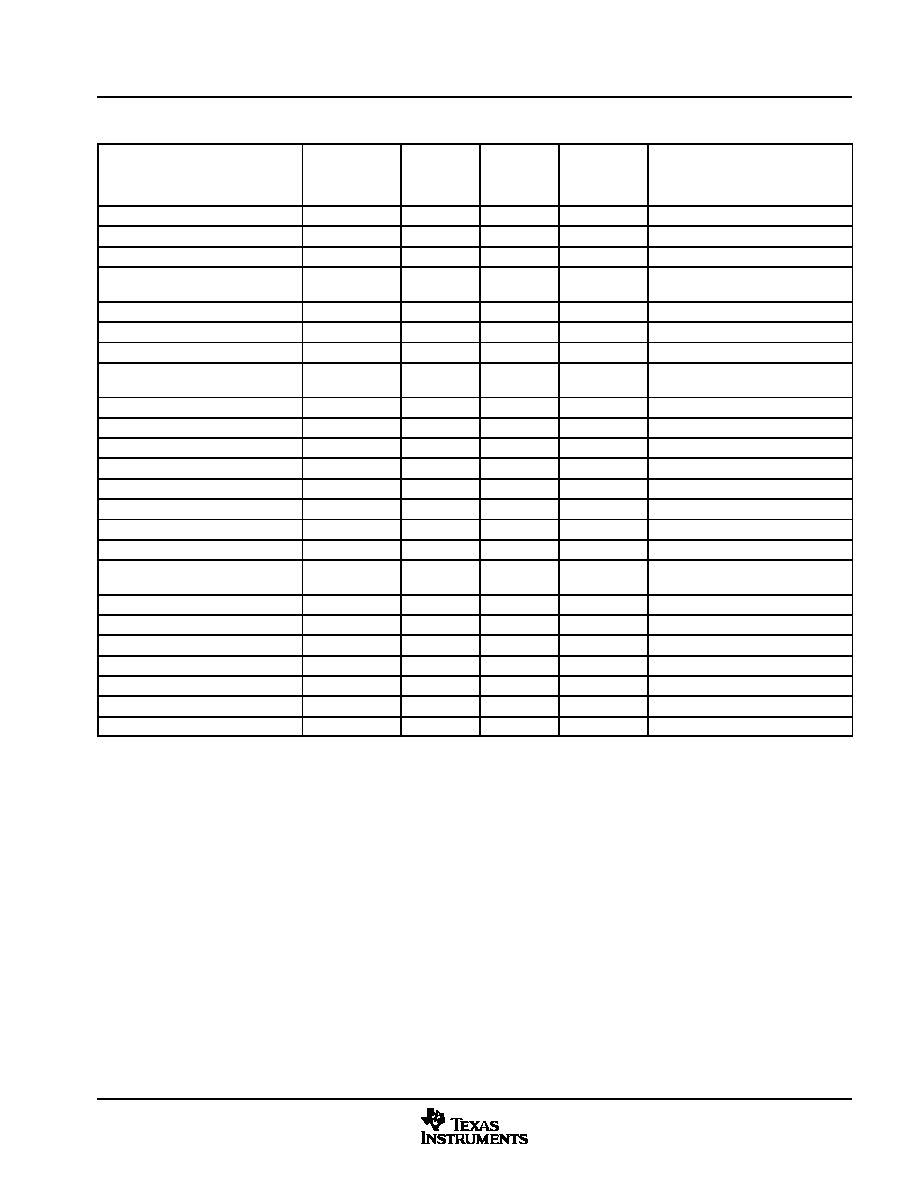
Functional Overview
115
August 2002 - Revised August 2004
SPRS197D
Table 3-74. DSP Level 1 Interrupt Mappings
INTERRUPT
DSP
INTERRUPT
DSP
IFR/IMR
REGISTER
BIT
VECTOR
LOCATION
(BYTE
ADDRESS)
PRIORITY
FUNCTION
RESET
-
-
FFF00h
0
DSP Reset Interrupt
NMI
-
-
FFF08h
1
DSP Nonmaskable Interrupt
EMULATOR_TEST
INT2
2
FFF10h
3
DSP Emulator/Test Interrupt
LEVEL2_INTH_FIQ
INT3
3
FFF18h
5
FIQ Interrupt From DSP Level 2
Handler
TC_ABORT
INT4
4
FFF20h
6
Traffic Controller Abort Interrupt
MAILBOX_1 (ARM2DSP1)
INT5
5
FFF28h
7
MPU-to-DSP Mailbox 1 Interrupt
Reserved
INT6
6
FFF30h
9
Unused, Keep Masked
GPIO
INT7
7
FFF38h
10
Interrupt for DSP-Owned Shared
GPIO
TIMER3
INT8
8
FFF40h
11
DSP Timer 3 Interrupt
DMA_CHANNEL_1
INT9
9
FFF48h
13
DSP DMA Channel 1 Interrupt
MPU
INT10
10
FFF50h
14
MPU Interrupt to DSP
Reserved
INT11
11
FFF58h
15
Unused, Keep Masked
UART3
INT12
12
FFF60h
17
UART Interrupt
WDGTIMER
INT13
13
FFF68h
18
DSP Watchdog Timer Interrupt
DMA_CHANNEL_4
INT14
14
FFF70h
21
DSP DMA Channel 4 Interrupt
DMA_CHANNEL_5
INT15
15
FFF78h
22
DSP DMA Channel 5 Interrupt
EMIF
INT16
16
FFF80h
4
Interrupt for DMA EMIF Interface to
Traffic Controller
LOCAL_BUS
INT17
17
FFF88h
8
Local Bus Interrupt
DMA_CHANNEL_0
INT18
18
FFF90h
12
DSP DMA Channel 0 Interrupt
MAILBOX2 (ARM2DSP2)
INT19
19
FFF98h
16
MPU-to-DSP Mailbox 2 Interrupt
DMA_CHANNEL_2
INT20
20
FFFA0h
19
DSP DMA Channel 2 Interrupt
DMA_CHANNEL_3
INT21
21
FFFA8h
20
DSP DMA Channel 3 Interrupt
TIMER2
INT22
22
FFFB0h
23
DSP Timer 2 Interrupt
TIMER1
INT23
23
FFFB8h
24
DSP Timer 1 Interrupt

Functional Overview
116
August 2002 - Revised August 2004
SPRS197D
Table 3-75. DSP Level 2 Interrupt Mappings
INTERRUPT
DEFAULT
SENSITIVITY
LEVEL 1
MAPPING
LEVEL 2
MAPPING
FUNCTION
MCBSP3_TX
Edge
INT3
IRQ_0
McBSP3 Transmit Interrupt
MCBSP3_RX
Edge
INT3
IRQ_1
McBSP3 Receive Interrupt
MCBSP1_TX
Edge
INT3
IRQ_2
McBSP1 Transmit Interrupt
MCBSP1_RX
Edge
INT3
IRQ_3
McBSP1 Receive Interrupt
UART2
Level
INT3
IRQ_4
UART2 Interrupt
UART1
Level
INT3
IRQ_5
UART1 Interrupt
MCSI1_TX
Level
INT3
IRQ_6
MCSI1 Transmit Interrupt
MCSI1_RX
Level
INT3
IRQ_7
MCSI1 Receive Interrupt
MCSI2_TX
Level
INT3
IRQ_8
MCSI2 Transmit Interrupt
MCSI2_RX
Level
INT3
IRQ_9
MCSI2 Receive Interrupt
MCSI1_FRAME_ERROR_INT
Level
INT3
IRQ_10
MCSI1 Frame Error Interrupt
MCSI2_FRAME_ERROR_INT
Level
INT3
IRQ_11
MCSI2 Frame Error Interrupt
Reserved
-
INT3
IRQ_12
Reserved, Keep Masked
Reserved
-
INT3
IRQ_13
Reserved, Keep Masked
Reserved
-
INT3
IRQ_14
Reserved, Keep Masked
Reserved
-
INT3
IRQ_15
Reserved, Keep Masked

Functional Overview
117
August 2002 - Revised August 2004
SPRS197D
3.18 MPU System DMA Request Mapping
Table 3-76 shows the MPU system DMA request mapping for the OMAP5910 device.
Table 3-76. DMA Request Mapping
MPU SYSTEM DMA REQUESTS
MPU SYSTEM DMA
MCSI1 TX
DMA_REQ_01
MCSI1 RX
DMA_REQ_02
I
2
C RX
DMA_REQ_03
I
2
C TX
DMA_REQ_04
EXT_DMA_REQ0 (MPUIO2)
DMA_REQ_05
EXT_DMA_REQ1 (MPUIO4)
DMA_REQ_06
MicroWire TX
DMA_REQ_07
McBSP1 TX
DMA_REQ_08
McBSP1 RX
DMA_REQ_09
McBSP3 TX
DMA_REQ_10
McBSP3 RX
DMA_REQ_011
UART1 TX
DMA_REQ_012
UART1 RX
DMA_REQ_013
UART2 TX
DMA_REQ_014
UART2 RX
DMA_REQ_015
McBSP2 TX
DMA_REQ_016
McBSP2 RX
DMA_REQ_017
UART3 TX
DMA_REQ_018
UART3 RX
DMA_REQ_019
Camera RX
DMA_REQ_020
MMC TX
DMA_REQ_021
MMC RX
DMA_REQ_022
Reserved
DMA_REQ_023
Reserved
DMA_REQ_024
Reserved
DMA_REQ_025
USB function RX0
DMA_REQ_026
USB function RX1
DMA_REQ_027
USB function RX2
DMA_REQ_028
USB function TX0
DMA_REQ_029
USB function TX1
DMA_REQ_030
USB function TX2
DMA_REQ_031

Functional Overview
118
August 2002 - Revised August 2004
SPRS197D
3.19 DSP DMA Event Mapping
Table 3-77 defines the mappings of the DMA channel synchronization settings to the different request sources
that can be used to create DSP DMA events on OMAP5910.
Table 3-77. DSP DMA Mapping
DSP REQUEST SOURCE
DSP DMA
REQUEST LINE
MCSI1 TX
DMA_REQ_01
MCSI1 RX
DMA_REQ_02
MCSI2 TX
DMA_REQ_03
MCSI2 RX
DMA_REQ_04
EXT_DMA_REQ0 (MPUIO2)
DMA_REQ_05
EXT_DMA_REQ1 (MPUIO4)
DMA_REQ_06
Reserved
DMA_REQ_07
McBSP1 TX
DMA_REQ_08
McBSP1 RX
DMA_REQ_09
McBSP3 TX
DMA_REQ_10
McBSP3 RX
DMA_REQ_011
UART1 TX
DMA_REQ_012
UART1 RX
DMA_REQ_013
UART2 TX
DMA_REQ_014
UART2 RX
DMA_REQ_015
Reserved
DMA_REQ_016
Reserved
DMA_REQ_017
UART3 TX
DMA_REQ_018
UART3 RX
DMA_REQ_019

Documentation Support
119
August 2002 - Revised August 2004
SPRS197D
4
Documentation Support
Extensive documentation supports all OMAP platform of devices from product announcement through
applications development. The following types of documentation are available to support the design and use
of the OMAP platform of dual-core processor devices:
�
Device-specific data sheets
�
Development-support tools
�
Hardware and software application reports
The OMAP5910 reference documentation includes, but is not limited to, the following:
�
TMS320C55x DSP CPU Programmer's Reference Supplement (literature number SPRU652)
�
OMAP5910 Dual-Core Processor Functional and Peripheral Overview (literature number SPRU602)
�
OMAP5910 Dual-Core Processor MPU Subsystems Reference Guide (literature number SPRU671)
�
OMAP5910 Dual-Core Processor DSP Subsystems Reference Guide (literature number SPRU672)
�
OMAP5910 Dual-Core Processor Memory Interface Traffic Controller Reference Guide (literature number
SPRU673)
�
OMAP5910 Dual-Core Processor System DMA Controller Reference Guide (literature number
SPRU674)
�
OMAP5910 Dual-Core Processor LCD Controller Reference Guide (literature number SPRU675)
�
OMAP5910 Dual-Core Processor Universal Asynchronous Receiver/Transmitter (UART) Devices
Reference Guide (literature number SPRU676)
�
OMAP5910 Dual-Core Processor Universal Serial Bus (USB) and Frame Adjustment Counter (FAC)
Reference Guide (literature number SPRU677)
�
OMAP5910 Dual-Core Processor Clock Generation and System Reset Management Reference Guide
(literature number SPRU678)
�
OMAP5910 Dual-Core Processor General-Purpose Input/Output (GPIO) Reference Guide (literature
number SPRU679)
�
OMAP5910 Dual-Core Processor MultiMedia Card/Secure Data Memory Card (MMC/SD) Reference
Guide (literature number SPRU680)
�
OMAP5910 Dual-Core Processor Inter-Integrated Circuit (I
2
C) Controller Reference Guide (literature
number SPRU681)
�
OMAP5910 Dual-Core Processor Timer Reference Guide (literature number SPRU682)
�
OMAP5910 Dual-Core Processor Inter-Processor Communication Reference Guide (literature number
SPRU683)
�
OMAP5910 Dual-Core Processor Camera Interface Reference Guide (literature number SPRU684)
�
OMAP5910 Dual-Core Processor Multichannel Serial Interface (MCSI) Reference Guide (literature
number SPRU685)
�
OMAP5910 Dual-Core Processor MicroWire Interface Reference Guide (literature number SPRU686)
�
OMAP5910 Dual-Core Processor Real-Time Clock (RTC) Reference Guide (literature number
SPRU687)
�
OMAP5910 Dual-Core Processor HDQ/1-Wire Interface Reference Guide (literature number SPRU688)
�
OMAP5910 Dual-Core Processor PWL, PWT, and LED Reference Guide (literature number SPRU689)
�
OMAP5910 Dual-Core Processor Multichannel Buffered Serial Port (McBSP) Reference Guide (literature
number SPRU708)
�
OMAP5910 Dual-Core Processor Silicon Errata (literature number SPRZ016)
A series of DSP textbooks is published by Prentice-Hall and John Wiley & Sons to support digital signal
processing research and education. The TMS320 DSP newsletter, Details on Signal Processing, is published
quarterly and distributed to update TMS320 DSP customers on product information.
Information regarding Texas Instruments (TI) OMAP and DSP products is also available on the Worldwide
Web at http://www.ti.com uniform resource locator (URL).
TMS320 and TMS320C5000 are trademarks of Texas Instruments.

Documentation Support
120
August 2002 - Revised August 2004
SPRS197D
4.1
Device and Development-Support Tool Nomenclature
To designate the stages in the product development cycle, TI assigns prefixes to the part numbers of all
OMAP processors and support tools. Each commercial OMAP platform member has one of three prefixes:
X, P, or null (no prefix). Texas Instruments recommends two of three possible prefix designators for its support
tools: TMDX and TMDS. These prefixes represent evolutionary stages of product development from
engineering prototypes (TMDX) through fully qualified production devices/tools (TMDS).
Device development evolutionary flow:
X
Experimental device that is not necessarily representative of the final device's electrical
specifications and may not use production assembly flow. (TMX definition)
P
Prototype device that is not necessarily the final silicon die and may not necessarily meet final
electrical specifications. (TMP definition)
null
Production version of the silicon die that is fully qualified. (TMS definition)
Support tool development evolutionary flow:
TMDX Development support product that has not yet completed Texas Instruments internal qualification
testing.
TMDS Fully qualified development support product
TMX and TMP devices and TMDX development-support tools are shipped against the following disclaimer:
"Developmental product is intended for internal evaluation purposes."
Production devices and TMDS development-support tools have been characterized fully, and the quality and
reliability of the device have been demonstrated fully. TI's standard warranty applies.
Predictions show that prototype devices (X or P), have a greater failure rate than the standard production
devices. Texas Instruments recommends that these devices not be used in any production system because
their expected end-use failure rate still is undefined. Only qualified production devices are to be used.
For additional description of the device nomenclature markings, see the OMAP5910 Dual-Core Processor
Silicon Errata (literature number SPRZ016).
PREFIX
TEMPERATURE RANGE
OMAP 5910
GZG S
DEVICE
NULL = -40�C to 85�C Case
C = 0�C to 85�C Case
PACKAGE TYPE
SPEED GRADE
2 = 150 MHz
X
SILICON REVISION
GZG = 289-pin MicroStar BGA
ZZG = Lead-Free 289-pin MicroStar BGA
GDY = 289-pin BGA
X Experimental device
P
P Prototype device
null Production device
Figure 4-1. OMAP Device Nomenclature

Electrical Specifications
121
August 2002 - Revised August 2004
SPRS197D
5
Electrical Specifications
This section provides the absolute maximum ratings and the recommended operating conditions for the
OMAP5910 device.
All electrical and switching characteristics in this data manual are valid over the recommended operating
conditions unless otherwise specified.
5.1
Absolute Maximum Ratings
The list of absolute maximum ratings are specified over operating case temperature. Stresses beyond those
listed under "absolute maximum ratings" may cause permanent damage to the device. These are stress
ratings only, and functional operation of the device at these or any other conditions beyond those indicated
under Section 5.2, Recommended Operating Conditions, is not implied. Exposure to
absolute-maximum-rated conditions for extended periods may affect device reliability. All supply voltage
values (core and I/O) are with respect V
SS
.
NOTE: The OMAP5910 device has undergone Charged Device Model Electrostatic Discharge
(ESD) testing, passing at the �500 V level. Human Body Model (HBM) ESD testing per
EIA/JESD22-A114 has also been performed. Test results indicate that the OMAP5910 passes
at a �500 V HBM (maximum) level. Caution in handling devices is advised.
This section provides the absolute maximum ratings for the OMAP5910 device.
Supply voltage range (core), CV
DD
,CV
DD1/2/3/4/A
-0.3 V to 1.8 V
. . . . . . . . . . . . . . . . . . . . . . . . . . . . . . . . .
Supply voltage range (I/O), DV
DD1/2/3/4/5
-0.3 V to 4 V
. . . . . . . . . . . . . . . . . . . . . . . . . . . . . . . . . . . . . . . . . .
Input voltage range, V
I
(12-MHz and 32-kHz oscillator)
-0.3 V to CV
DD
+ 0.5 V
. . . . . . . . . . . . . . . . . . . . .
Input voltage range, V
I
(standard LVCMOS)
-0.3 V to DV
DD
+ 0.5 V
. . . . . . . . . . . . . . . . . . . . . . . . . . . . . . .
Input voltage range, V
I
(fail-safe LVCMOS)
-0.3 V to 4.5 V
. . . . . . . . . . . . . . . . . . . . . . . . . . . . . . . . . . . . . . .
Input voltage range, V
I
(USB transceivers)
-0.3 V to DV
DD
+ 0.5 V
. . . . . . . . . . . . . . . . . . . . . . . . . . . . . . . .
Input voltage range, V
I
(I
2
C)
-0.3 V to 4.5 V
. . . . . . . . . . . . . . . . . . . . . . . . . . . . . . . . . . . . . . . . . . . . . . . . . . .
Output voltage range, V
O
(standard LVCMOS)
-0.3 V to DV
DD
+ 0.5 V
. . . . . . . . . . . . . . . . . . . . . . . . . . . .
Output voltage range, V
O
(fail-safe LVCMOS)
-0.3 V to 4.5 V
. . . . . . . . . . . . . . . . . . . . . . . . . . . . . . . . . . . .
Output voltage range, V
O
(USB transceivers)
-0.3 V to DV
DD
+ 0.5 V
. . . . . . . . . . . . . . . . . . . . . . . . . . . . . .
Output voltage range, V
O
(I
2
C)
-0.3 V to 4.5 V
. . . . . . . . . . . . . . . . . . . . . . . . . . . . . . . . . . . . . . . . . . . . . . . . .
Operating temperature range, T
C
-40�C to 85�C
. . . . . . . . . . . . . . . . . . . . . . . . . . . . . . . . . . . . . . . . . . . . . . .
Storage temperature range, T
stg
-55�C to 150�C
. . . . . . . . . . . . . . . . . . . . . . . . . . . . . . . . . . . . . . . . . . . . . . .

Electrical Specifications
122
August 2002 - Revised August 2004
SPRS197D
5.2
Recommended Operating Conditions
MIN
NOM
MAX
UNIT
CV
DD
Device supply voltage core
Low Power Standby mode
1
1.1
1.675
V
CV
DD
CV
DD1/2/3/4/A
Device supply voltage, core
Active mode
1.525
1.6
1.675
V
DV
DD1
Device supply voltage, I/O (Peripheral I/O)
2.5
2.75 or 3.3
3.6
V
DV
DD2
Device supply voltage, I/O (USB transceiver)
3
3.3
3.6
V
DV
Device supply voltage, I/O
Low-voltage range
�
1.65
1.8
1.95
V
DV
DD3
Device supply voltage, I/O
(MCSI2, McBSP2, GPIO[9:8])
High-voltage range
�
2.5
2.75 or 3.3
3.6
V
DV
Device supply voltage, I/O
Low-voltage range
�
1.65
1.8
1.95
V
DV
DD4
Device supply voltage, I/O
(SDRAM interface)
High-voltage range
�
2.5
2.75 or 3.3
3.6
V
DV
Device supply voltage, I/O
Low-voltage range
�
1.65
1.8
2
V
DV
DD5
Device supply voltage, I/O
(FLASH interface)
High-voltage range
�
2.5
2.75 or 3.3
3.6
V
CV
DD
-
DV
DD
Device supply voltage difference
�
1.65
V
DV
DD
- CV
DD
Device supply voltage difference
�
2.6
V
V
SS
Supply voltage, GND
0
V
Standard LVCMOS
0.7 DV
DD
DV
DD
V
High level input voltage I/O
Fail-safe LVCMOS
0.7 DV
DD
DV
DD
V
V
IH
High-level input voltage, I/O
USB.DP, DM (mode 1)
2
DV
DD
V
I
2
C
0.7 DV
DD
DV
DD
Standard LVCMOS
0
0.3 DV
DD
V
Low level input voltage I/O
Fail-safe LVCMOS
0
0.3 DV
DD
V
V
IL
Low-level input voltage, I/O
USB.DP, DM (mode 1)
0
0.8
V
I
2
C
0
0.3 DV
DD
V
Input voltage
USB.DP, DM (mode 2)
0.8
2.5
V
V
I
Input voltage
OSC1 and OSC32K pins
CV
DD
V
V
ID
Differential input voltage, I/O
USB.DP, DM (mode 2)
200
mV
2-mA drive strength buffers
-2
4-mA drive strength buffers
-4
I
OH
High-level output current
8-mA drive strength buffers
-8
mA
OH
g
p
18.3-mA drive strength
buffers
-18.3
2-mA drive strength buffers
2
4-mA drive strength buffers
4
I
OL
Low-level output current
6-mA drive strength buffers
6
mA
I
OL
Low-level output current
8-mA drive strength buffers
8
mA
18.3-mA drive strength
buffers
18.3
T
C
Operating case temperature
-40
85
�C
All core voltage supplies should be tied to the same voltage level (within 0.3 V).
Low Power Standby is defined as follows: the device is in Deep Sleep mode and LOW_PWR = 1. The device runs from 32 kHz clock in this mode.
�
High and low voltage ranges are selectable via software configuration.
�
In systems where the CV
DDx
and DV
DDx
power supplies are ramped at generally the same time (within 500 ms of one another), there are no
specific power sequencing requirements for the supplies. The only sequencing requirement is that the maximum voltage difference between
CV
DD
and DV
DD
is not exceeded for greater than 500 ms. Likewise, if different voltages are used for the separate DV
DDx
supplies, all DV
DDx
supplies should be ramp up to valid voltage levels within 500 ms of one another.

Electrical Specifications
123
August 2002 - Revised August 2004
SPRS197D
5.3
Electrical Characteristics Over Recommended Operating Case Temperature
Range (Unless Otherwise Noted)
PARAMETER
TEST CONDITIONS
MIN
TYP
MAX UNIT
Hi h l
l t t
Standard LVCMOS
DV
DD
= 3.3 V, I
OH
= MAX
0.8 DV
DD
V
OH
High-level output
voltage
Fail-safe LVCMOS
DV
DD
= 3.3 V, I
OH
= MAX
0.8 DV
DD
V
V
OH
voltage
USB.DP, DM
I
O
= -12 mA
DV
DD
- 0.5
V
Standard LVCMOS
DV
DD
= 3.3 V, I
OL
= MAX
0.22 DV
DD
Fail-safe LVCMOS
DV
DD
= 3.3 V, I
OL
= MAX
0.22 DV
DD
Low level output
USB.DP, DM
I
O
= 12 mA
0.5
V
OL
Low-level output
voltage
Fast mode at 6-mA load
0.6
V
OL
voltage
I
2
C
Fast mode at 3-mA load
0.4
I
2
C
Standard mode at 3-mA
load
0.4
Fail-safe LVCMOS inputs
without internal
pullups/pulldowns enabled
V
I
= V
I
MAX to V
I
MIN
- 20
20
Other Inputs without internal
pullups/pulldowns enabled
V
I
= V
I
MAX to V
I
MIN
-1
1
I
I
Input current
Input pins with 20-�A
pulldowns enabled
DV
DD
= MAX,
V
I
= V
SS
to V
DD
6
20
60
�A
I
I
Input current
Input pins with 100-�A
pulldowns enabled
DV
DD
= MAX,
V
I
= V
SS
to V
DD
30
100
300
�A
Input pins with 20-�A
pullups enabled
CV
DD
= MAX,
V
I
= V
SS
to V
DD
- 60
- 20
- 6
Input pins with 100-�A
pullups enabled
DV
DD
= MAX,
V
I
= V
SS
to V
DD
- 300
- 100
- 30
I
OZ
Input current for outputs in high-impedance
- 20
20
�A
I
Core voltage supply current quiescent
Sum of CV
DDx
currents.
(Deep sleep mode
with CV
DD
= 1.6 V)
210
�A
I
DDC (Q)
Core voltage supply current, quiescent
Sum of CV
DDx
currents.
(Deep sleep mode
with CV
DD
= 1.1 V)
110
�A
I
Core voltage supply current active
Sum of CV
DDx
currents
(Case 1
).
150
mA
I
DDC (A)
Core voltage supply current, active
Sum of CV
DDx
currents
(Case 2
).
170
mA
I
Core and I/O voltage supply current active
Sum of CV
DDx
and DV
DDx
currents (Case 3
�
).
45
mA
I
DDCP (A)
Core and I/O voltage supply current, active
Sum of CV
DDx
and DV
DDx
currents (Case 4
�
).
6
mA
C
Input capacitance
USB.DP,DM
7
pF
C
i
Input capacitance
All other I/O pins
4
pF
C
Output capacitance
USB.DP,DM
7
pF
C
O
Output capacitance
All other I/O pins
4
pF
Case 1: MPU running OS, DSP running GSM Vocoder from internal memory, DSP MMU and all clock domains active, no LCD activity.
Case 2: Same conditions as Case 1 only DSP running from external memory with I-cache enabled.
�
Case 3: Only LCD activity (MPU and DSP idled with clocks off). LCD running 320x240 TFT at 70 Frames per second with frame buffer in internal
memory (DPLL at 120 MHz).
�
Case 4: Same as Case 3 only LCD running at 10 Frames per second with DPLL at 6MHz.

Electrical Specifications
124
August 2002 - Revised August 2004
SPRS197D
Transmission Line
4.0 pF
1.85 pF
Z0 = 50 W
(see note)
Tester Pin Electronics
Data Sheet Timing Reference Point
Output
Under
Test
NOTE: The data sheet provides timing at the device pin. For output timing analysis, the tester pin electronics and its transmission line effects
must taken into account. A transmission line with a delay of 2 ns or longer can be used to produce the desired transmission line effect.
The transmission line is intended as a load only. It is not necessary to add or subtract the transmission line delay (2 ns or longer) from
the data sheet timings.
42 W
3.5 nH
Device Pin
(see note)
Input requirements in this data sheet are tested with an input slew rate of < 4 Volts per nanosecond (4 V/ns) at the device pin.
Figure 5-1. Tester Pin Electronics
5.4
Package Thermal Resistance Characteristics
Table 5-1 provides the thermal resistance characteristics for the package types available for use on the
OMAP5910 device.
Table 5-1. Thermal Resistance Characteristics
R
JA
(�C/W)
R
JC
(�C/W)
PACKAGE TYPE
32.77
10.76
289GZG
25.54
10.11
289GDY
5.5
Timing Parameter Symbology
Timing parameter symbols used in the timing requirements and switching characteristics tables are created
in accordance with JEDEC Standard 100. To shorten the symbols, some of the pin names and other related
terminology have been abbreviated as follows:
Lowercase subscripts and their meanings:
Letters and symbols and their meanings:
a
access time
H
High
c
cycle time (period)
L
Low
d
delay time
V
Valid
dis
disable time
Z
High impedance
en
enable time
f
fall time
h
hold time
r
rise time
su
setup time
t
transition time
v
valid time
w
pulse duration (width)
X
Unknown, changing, or don't care level
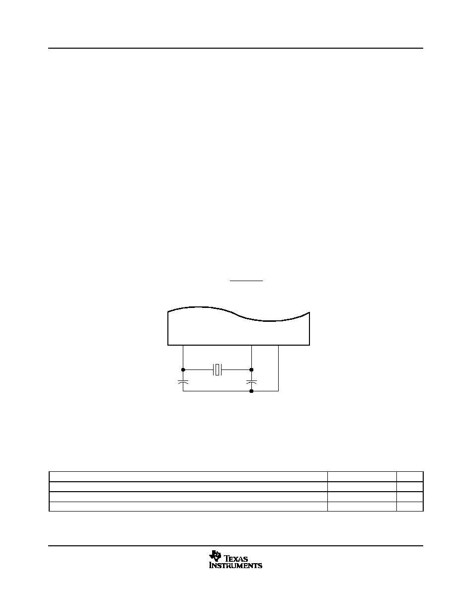
Electrical Specifications
125
August 2002 - Revised August 2004
SPRS197D
5.6
Clock Specifications
This section provides the timing requirements and switching characteristics for the OMAP5910 system clock
signals.
5.6.1 32-kHz Oscillator and Input Clock
The 32.768-kHz clock signal (often abbreviated to 32-kHz) may be supplied by either the on-chip 32-kHz
oscillator (requiring an external crystal) or an external CMOS signal. The state of the CLK32K_CTRL pin
determines which is used.
The on-chip oscillator requires an external 32.768-kHz crystal connected across the OSC32K_IN and
OSC32K_OUT pins. The connection of the required circuit, consisting of the crystal and two load capacitors,
is shown in Figure 5-2. The load capacitors, C
1
and C
2
, should be chosen such that the equation below is
satisfied (recommended values are C
1
= C
2
= 10 pF). C
L
in the equation is the load specified for the crystal.
All discrete components used to implement the oscillator circuit should be placed as close as possible to the
associated oscillator pins (OSC32K_IN and OSC32K_OUT) and to the V
SS
pin closest to the oscillator pins
(GZG ball V12 or GDY ball F6).
NOTE: The 32.768-kHz oscillator is powered by the CV
DD
supply. If an external clock source is used instead
of using the on-chip oscillator, care must be taken that the voltage level driven onto the OSC32K_IN and
OSC32K_OUT pins is no greater than the CV
DD
voltage level.
C
L
+
C
1
C
2
(C
1
) C
2
)
OSC32K_IN
OSC32K_OUT
C1
C2
Crystal
V
SS
32.768 kHz
Figure 5-2. 32-kHz Oscillator External Crystal
Table 5-2 shows the switching characteristics of the 32-kHz oscillator and Table 5-3 shows the input
requirements of the 32-kHz clock input.
Table 5-2. 32-kHz Oscillator Switching Characteristics
PARAMETER
MIN
TYP
MAX
UNIT
Start-up time (from power up until oscillating at stable frequency of 32.768 kHz)
200
800
ms
I
DDA
, active current consumption
4
�A
Oscillation frequency
32.768
kHz

Electrical Specifications
126
August 2002 - Revised August 2004
SPRS197D
Table 5-3. 32-kHz Input Clock Timing Requirements
NO.
MIN
NOM
MAX
UNIT
CK1
t
cyc
Frequency
32.768
kHz
CK2
t
f
Fall time
25
ns
CK3
t
r
Rise time
25
ns
CK4
Duty cycle (high-to-low ratio)
30%
70%
%
CK5
Frequency stability
-70
70
ppm
CK1
CK2
CK3
CLK32K_IN
Figure 5-3. 32-kHz Input Clock
5.6.2 Base Oscillator (12 MHz or 13 MHz) and Input Clock
The internal base system oscillator is enabled following a device reset. The oscillator requires an external
crystal to be connected across the OSC1_IN and OSC1_OUT pins. If the internal oscillator is not used
(configured in software using FUNC_MUX_CTRL_B register), an external clock source must be applied to the
OSC1_IN pin and the OSC1_OUT pin must be left unconnected. Because the internal oscillator can be used
as a clock source to the OMAP DPLL, the 12- or 13-MHz crystal oscillation frequency can be multiplied to
generate the DSP clock, MPU clock, traffic controller clock.
The crystal must be in fundamental-mode operation, and parallel resonant, with a maximum effective series
resistance of 60 maximum. The connection of the required circuit, consisting of the crystal and two load
capacitors, is shown in Figure 5-4. The load capacitors, C
1
and C
2
, must be chosen such that the equation
below is satisfied (recommended values are C
1
= C
2
= 10 pF). C
L
in the equation is the load specified for the
crystal. All discrete components used to implement the oscillator circuit must be placed as close as possible
to the associated oscillator pins (OSC1_IN and OSC1_OUT) and to the V
SS
pins closest to the oscillator pins
(GZG balls AA1/Y3 or GDY balls E13/K9).
NOTE: The base oscillator is powered by the CV
DD
supply. If an external clock source is used instead of using
the on-chip oscillator, care must be taken that the voltage level driven onto the OSC1_IN pin is no greater than
the CV
DD
voltage level.
C
L
+
C
1
C
2
(C
1
) C
2
)
OSC1_IN
OSC1_OUT
C1
C2
12 or 13 MHz crystal
Figure 5-4. Internal System Oscillator External Crystal
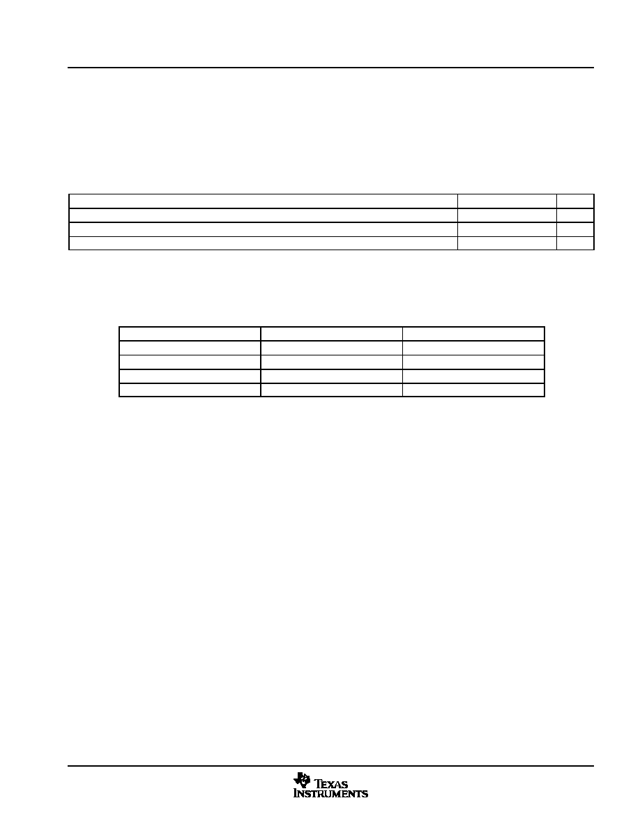
Electrical Specifications
127
August 2002 - Revised August 2004
SPRS197D
If USB host function is used, it is recommended that a very low PPM crystal ( 50 ppm) be used for the
12- or 13-MHz oscillator circuit. If the USB host function is not used, then a crystal of 180 ppm is
recommended. When selecting a crystal, the system design must take into account the temperature and aging
characteristics of a crystal versus the user environment and expected lifetime of the system.
Table 5-4 shows the switching characteristics of the base oscillator.
Table 5-4. Base Oscillator Switching Characteristics
PARAMETER
MIN
TYP
MAX
UNIT
Start-up time (from power up until oscillating at stable frequency of 12 or 13 MHz)
1
4
ms
I
DDA
, active current consumption
350
�A
Oscillation frequency
12 or 13
MHz
5.6.3 Internal Clock Speed Limitations
Table 5-5 provides a summary of the maximum frequencies that each clock domain may be configured to run
on the OMAP5910 device.
Table 5-5. Internal Clock Speed Limitations
CLOCK
MAX OPERATING FREQUENCY
UNIT
MPU (CLKM1)
150
MHz
DSP (CLKM2)
150
MHz
TC (CLKM3)
75
MHz
DPLL1
150
MHz
All clock domains must be derived from the same DPLL1 frequency setting; therefore, the following conditions
must be satisfied where `m', `n', and `o' are each equal to either 1, 2, 4, or 8:
�
MPU frequency = (DPLL1 clock frequency) / m
�
DSP frequency = (DPLL1 clock frequency) / n
�
TC frequency = (DPLL1 clock frequency) / o
For example, the following configuration is valid:
�
MPU/DSP/TC = 150 MHz/150 MHz/75 MHz, where m = n = 1 and o = 2
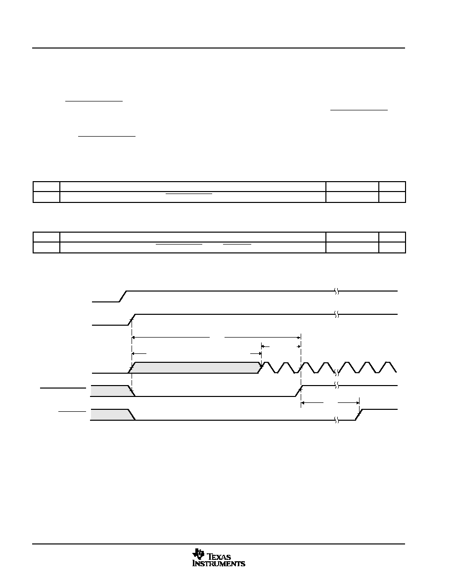
Electrical Specifications
128
August 2002 - Revised August 2004
SPRS197D
5.7
Reset Timings
This section provides the timing requirements for the OMAP5910 hardware reset signals.
5.7.1 OMAP5910 Device Reset
The PWRON_RESET signal is the active-low asynchronous reset input responsible for the reset of the entire
OMAP5910 device. When using an external crystal to supply the 32-kHz system clock, PWRON_RESET must
be asserted low a minimum of two 32-kHz clock cycles longer than the worst-case start-up time of the 32-kHz
oscillator after stable power supplies (see Figure 5-5). If an external CMOS input signal is used to source
32 kHz, PWRON_RESET must be asserted low a minimum of two 32-kHz clock cycles after stable power
supplies. See Table 5-6 and Table 5-7.
Table 5-6. OMAP5910 Device Reset Timing Requirements
NO.
MIN
MAX
UNIT
RS1
t
w(PWRON_RST)
Pulse duration, PWRON_RESET low
800
ms
Table 5-7. OMAP5910 Device Reset Switching Characteristics
NO.
PARAMETER
MIN
MAX
UNIT
RS2
t
d(PWRONH-RSTH)
Delay time, PWRON_RESET high to RST_OUT high
T + 10
�s
P = period of 32-kHz clock, C = Value of ULPD wakeup time setup register, SETUP_ULPD1_REG (Default 03FFh), T = P*C
CV
DDx
DV
DDx
OSC32K_IN
PWRON_RESET
RS1
RST_OUT
RS2
Worst-case Oscillator Start-up Time
2 Cycles
Figure 5-5. Device Reset Timings

Electrical Specifications
129
August 2002 - Revised August 2004
SPRS197D
5.7.2 OMAP5910 MPU Core Reset
The MPU_RST signal is the active-low asynchronous input responsible for the reset of the OMAP5910 MPU
core. Stable power supplies are assumed prior to MPU_RST assertion. Table 5-6 illustrates the behavior of
MPU_RST and RST_OUT. In Table 5-7, a logic high level is assumed on the PWRON_RESET input. In the case
where an application ties the PWRON_RESET and MPU_RST together, the behavior described in
Section 5.7.1, OMAP5910 Device Reset, will override. See Table 5-8 and Table 5-9.
Table 5-8. MPU_RST Timing Requirements
NO.
MIN
MAX
UNIT
M3
t
w(MPU_RST)
Pulse duration, MPU_RST low
50
�s
Table 5-9. MPU_RST Switching Characteristics
NO.
PARAMETER
MIN
MAX
UNIT
M1
t
d(MPUL-RSTL)
Delay time, MPU_RST low to RST_OUT low
1
�s
M2
t
Delay time MPU RST high to RST OUT high
MPU_RST asserted during
OMAP5910 awake state
10
�s
M2
t
d(MPUH-RSTH)
Delay time, MPU_RST high to RST_OUT high
MPU_RST asserted during
OMAP5910 deep sleep state
T + 10
�s
P = period of 32-kHz clock, C = Value of ULPD wakeup time setup register, SETUP_ULPD1_REG (Default 03FFh), T = P*C
MPU_RST
RST_OUT
M1
M2
M3
Figure 5-6. MPU Core Reset Timings

Electrical Specifications
130
August 2002 - Revised August 2004
SPRS197D
5.8
External Memory Interface Timing
5.8.1 EMIFS/Flash Interface Timing
Table 5-10 and Table 5-11 assume testing over recommended operating conditions
(see Figure 5-7 through
Figure 5-11).
Table 5-10. EMIFS/Flash Interface Timing Requirements
NO.
DV
DD5
= 1.8 V
Nominal
DV
DD5
= 2.75 V
Nominal
DV
DD5
= 3.3 V
Nominal
UNIT
NO.
MIN MAX
MIN MAX
MIN MAX
UNIT
F6
t
Setup time, read data valid Async modes
9
9
9
ns
F6
t
su(DV-CLKH)
Setup time, read data valid
before FLASH.CLK high
Sync Modes
3
3
3
ns
F7
t
Hold time, read data valid
Async modes
0
0
0
ns
F7
t
h(CLKH-RDV)
Hold time, read data valid
after FLASH.CLK high
Sync Modes
2
2
2
ns
The external FLASH.CLK is disabled for async modes. Async modes are only supported with the RT bit in the EMIFS configuration register set
to 0.
Sync modes are only supported with the RT bit in the EMIFS configuration register set to 1.
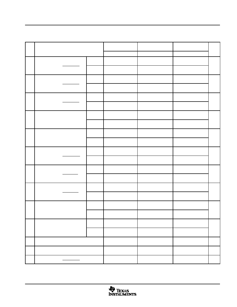
Electrical Specifications
131
August 2002 - Revised August 2004
SPRS197D
Table 5-11. EMIFS/Flash Interface Switching Characteristics
NO.
PARAMETER
DV
DD5
= 1.8 V
Nominal
DV
DD5
= 2.75 V
Nominal
DV
DD5
= 3.3 V
Nominal
UNIT
NO.
PARAMETER
MIN
MAX
MIN
MAX
MIN
MAX
UNIT
F1
t
Delay time,
FLASH.CLK high
Async
Modes
1
24
1
21
1
11
ns
F1
t
d(CLKH-CSV)
FLASH.CLK high
to FLASH.CSx
transition
Sync
Modes
-1
12
-1
10
-1
11
ns
F2
t
Delay time,
FLASH.CLK high
Async
Modes
1
24
1
21
1
20
ns
F2
t
d(CLKH-BEV)
FLASH.CLK high
to FLASH.BEx
valid
Sync
Modes
-1
12
-1
10
-1
11
ns
F3
t
Delay time,
FLASH.CLK high
Async
Modes
1
24
1
21
1
20
ns
F3
t
d(CLKH-BEIV)
FLASH.CLK high
to FLASH.BEx
invalid
Sync
Modes
-1
12
-1
10
-1
11
ns
F4
t
Delay time,
FLASH CLK high
Async
Modes
1
24
1
21
1
20
ns
F4
t
d(CLKH-AV)
FLASH.CLK high
to address valid
Sync
Modes
-1
8
0
7
0
7
ns
F5
t
Delay time,
FLASH CLK high
Async
Modes
1
24
1
21
1
20
ns
F5
t
d(CLKH-AIV)
FLASH.CLK high
to address invalid
Sync
Modes
-1
8
0
7
0
7
ns
F8
t
Delay time,
FLASH.CLK high
Async
Modes
1
24
1
21
1
20
ns
F8
t
d(CLKH-ADV)
FLASH.CLK high
to FLASH.ADV
transition
Sync
Modes
-1
12
-1
10
-1
11
ns
F9
t
Delay time,
FLASH.CLK high
Async
Modes
1
24
1
21
1
20
ns
F9
t
d(CLKH-OEV)
FLASH.CLK high
to FLASH.OE
transition
Sync
Modes
-1
12
-1
10
-1
11
ns
F12 t
Delay time,
FLASH.CLK high
Async
Modes
1
24
1
21
1
20
ns
F12 t
d(CLKH-WEV)
FLASH.CLK high
to FLASH.WE
transition
Sync
Modes
-1
12
-1
10
-1
11
ns
F13 t
Delay time,
FLASH CLK high
Async
Modes
1
24
1
21
1
20
ns
F13 t
d(CLKH-WDV)
FLASH.CLK high
to write data valid
Sync
Modes
1
22
1
20
1
18
ns
F14 t
Delay time,
FLASH.CLK high
Async
Modes
1
24
1
21
1
20
ns
F14 t
d(CLKH-WDIV)
FLASH.CLK high
to write data
invalid
Sync
Modes
1
22
1
20
1
18
ns
F15 t
d(CLKH-DHZ)
Delay time, FLASH.CLK high
to data bus high-impedance
24
21
20
ns
F16 t
d(CLKH-DLZ)
Delay time, FLASH.CLK high
to data bus driven
1
24
1
21
1
20
ns
F17 t
d(CLKH-BAAV)
Delay time, FLASH.CLK high
to FLASH.BAA transition
-1 + 0.5P
8 + 0.5P -1 + 0.5P 7.5 + 0.5P -1 + 0.5P 7.5 + 0.5P
ns
Data is referenced to the internal FLASH.CLK. The external FLASH.CLK is disabled for async modes.
P = period of undivided Traffic Controller clock regardless of FLASH.CLK divider configuration

Electrical Specifications
132
August 2002 - Revised August 2004
SPRS197D
F1
F2
F4
F8
F9
F9
F8
F7
F6
F5
F3
F1
D1
Valid
A1
FLASH.CLK
FLASH.CSx
FLASH.BE[1:0]
FLASH.A[24:1]
FLASH.D[15:0]
FLASH.ADV
FLASH.OE
FLASH.WE
(internal)
N cycles
FLASH.CLK is not driven during this mode of operation. The signal shown represents the internal FLASH.CLK signal given as a reference to
express relative timings.
Number of cycles is configurable via EMIFS setup registers.
Figure 5-7. Asynchronous Memory Read Timing

Electrical Specifications
133
August 2002 - Revised August 2004
SPRS197D
F1
F2
F4
F8
F9
F9
F8
F7
F6
F5
F3
F1
D1 upper
Valid
A1
FLASH.CLK
FLASH.CSx
FLASH.BE[1:0]
FLASH.A[24:1]
FLASH.D[15:0]
FLASH.ADV
FLASH.OE
FLASH.WE
F6
F7
D1 lower
(internal)
M cycles
N cycles
FLASH.CLK is not driven during this mode of operation. The signal shown represents the internal FLASH.CLK signal given as a reference to
express relative timings.
Number of cycles is configurable via EMIFS setup registers.
Figure 5-8. Asynchronous 32-Bit Read

Electrical Specifications
134
August 2002 - Revised August 2004
SPRS197D
F1
F2
F4
F8
F9
F9
F8
F7
F6
F5
F3
F1
D4
Valid
A1
FLASH.CLK
FLASH.CSx
FLASH.BE[1:0]
FLASH.A[24:3]
FLASH.D[15:0]
FLASH.ADV
FLASH.OE
FLASH.WE
F6
F7
D1
FLASH.A[2:1]
D2
D3
Word 0
Word 1
Word 2
Word 3
F5
F5
F4
F4
(internal)
M cycles
P cycles
P cycles
P cycles
FLASH.CLK is not driven during this mode of operation. The signal shown represents the internal FLASH.CLK signal given as a reference to
express relative timings.
Number of cycles is configurable via EMIFS setup registers.
Figure 5-9. Asynchronous Read - Page Mode ROM
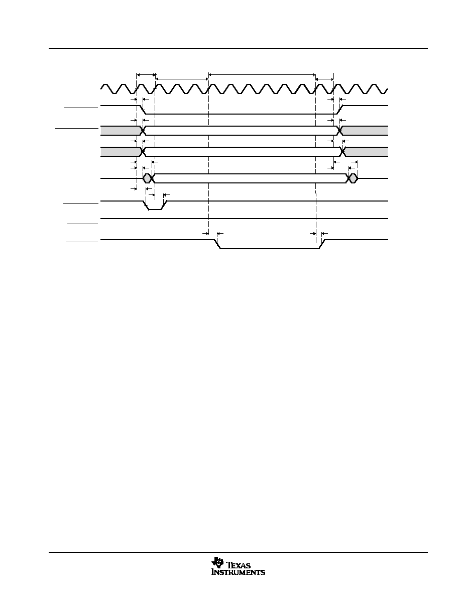
Electrical Specifications
135
August 2002 - Revised August 2004
SPRS197D
F1
F2
F4
F5
F3
F1
Valid
A1
FLASH.CLK
FLASH.CSx
FLASH.BE[1:0]
FLASH.A[24:1]
FLASH.D[15:0]
FLASH.ADV
FLASH.OE
FLASH.WE
F15
F14
F16
F13
F8
F8
F12
F12
D1
(internal)
P cycles
N cycles
M cycles
Q cycles
ADV width
WE width
CS hold
Wait-states
FLASH.CLK is not driven during this mode of operation. The signal shown represents the internal FLASH.CLK signal given as a reference to
express relative timings.
Number of cycles is configurable via EMIFS setup registers.
Figure 5-10. Asynchronous Memory Write Timing

Electrical Specifications
136
August 2002 - Revised August 2004
SPRS197D
Valid
A1
FLASH.CLK
FLASH.CSx
FLASH.BE[1:0]
FLASH.A[24:1]
FLASH.D[15:0]
FLASH.ADV
FLASH.BAA
F1
F2
F1
F3
F4
F5
D1
D2
D3
D4
F6
F7
F6
F7
F8
F8
F17
F17
F9
F9
FLASH.OE
FLASH.WE
N cycles
M cycles
ADV width
Wait-states
Q cycles
CLK start
(external)
FLASH.CLK is only driven during the active portion of the cycle. For reference, the dashed line shows FLASH.CLK as if it were continuous.
Number of cycles is configurable via EMIFS setup registers.
Figure 5-11. Synchronous Burst Read

Electrical Specifications
137
August 2002 - Revised August 2004
SPRS197D
5.8.2 EMIFF/SDRAM Interface Timing
Table 5-12 and Table 5-13 assume testing over recommended operating conditions
(see Figure 5-12
through Figure 5-17).
Table 5-12. EMIFF/SDRAM Interface Timing Requirements
NO.
DV
DD4
= 1.8 V
Nominal
DV
DD4
= 2.75 V
Nominal
DV
DD4
= 3.3 V
Nominal
UNIT
NO.
MIN
MAX
MIN
MAX
MIN
MAX
UNIT
SD7
t
su(DV-CLKH)
Setup time, read data valid before
SDRAM.CLK high
2
2
2
ns
SD8
t
h(CLKH-DV)
Hold time, read data valid after
SDRAM.CLK high
1
1
1
ns
Timing requirements are with the SD_RET field equal to 1 in the EMIFF configuration register.
Table 5-13. EMIFF/SDRAM Interface Switching Characteristics
NO.
PARAMETER
DV
DD4
= 1.8 V
Nominal
DV
DD4
= 2.75 V
Nominal
DV
DD4
= 3.3 V
Nominal
UNIT
NO.
PARAMETER
MIN
MAX
MIN
MAX
MIN
MAX
UNIT
SD1
t
c(CLK)
Cycle time, SDRAM.CLK
H
H
H
ns
SD2
t
w(CLK)
Pulse duration, SDRAM.CLK high/low
2.5
2.5
2.5
ns
SD3
t
d(CLKH-DQMV)
Delay time, SDRAM.CLK high to
SDRAM.DQMx valid
1.5
9
1.5
9
1.5
9
ns
SD4
t
d(CLKH-DQMIV)
Delay time, SDRAM.CLK high to
SDRAM.DQMx invalid
1.5
9
1.5
9
1.5
9
ns
SD5
t
d(CLKH-AV)
Delay time, SDRAM.CLK high to
SDRAM.A[12:0] address valid
1.5
9
1.5
9
1.5
9
ns
SD6
t
d(CLKH-AIV)
Delay time, SDRAM.CLK high to
SDRAM.A[12:0] address invalid
1.5
9
1.5
9
1.5
9
ns
SD9
t
d(CLKH-SDCASL)
Delay time, SDRAM.CLK high to
SDRAM.CAS low
1.5
9
1.5
9
1.5
9
ns
SD10 t
d(CLKH-SDCASH)
Delay time, SDRAM.CLK high to
SDRAM.CAS high
1.5
9
1.5
9
1.5
9
ns
SD11 t
d(CLKH-DV)
Delay time, SDRAM.CLK high to
SDRAM.D[15:0] data valid
1.5
9
1.5
9
1.5
9
ns
SD12 t
d(CLKH-DIV)
Delay time, SDRAM.CLK high to
SDRAM.D[15:0] data invalid
1.5
9
1.5
9
1.5
9
ns
SD13 t
d(CLKH-SDWEL)
Delay time, SDRAM.CLK high to
SDRAM.WE low
1.5
9
1.5
9
1.5
9
ns
SD14 t
d(CLKH-SDWEH)
Delay time, SDRAM.CLK high to
SDRAM.WE high
1.5
9
1.5
9
1.5
9
ns
SD15 t
d(CLKH-BAV)
Delay time, SDRAM.CLK high to
SDRAM.BA[1:0] valid
1.5
9
1.5
9
1.5
9
ns
SD16 t
d(CLKH-BAIV)
Delay time, SDRAM.CLK high to
SDRAM.BA[1:0] invalid
1.5
9
1.5
9
1.5
9
ns
SD17 t
d(CLKH-RASL)
Delay time, SDRAM.CLK high to
SDRAM.RAS low
1.5
9
1.5
9
1.5
9
ns
SD18 t
d(CLKH-RASH)
Delay time, SDRAM.CLK high to
SDRAM.RAS high
1.5
9
1.5
9
1.5
9
ns
H = 1/2 CPU cycle.
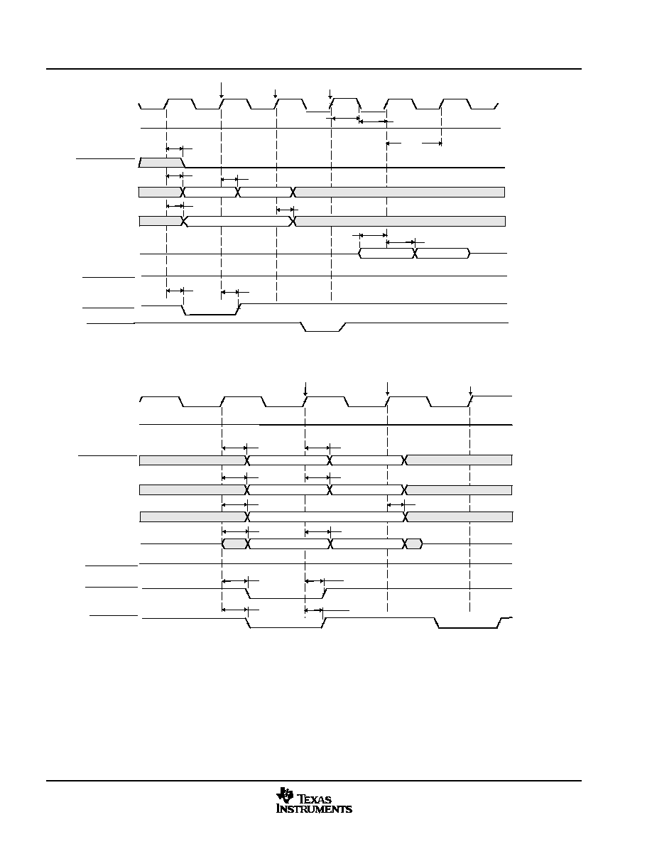
Electrical Specifications
138
August 2002 - Revised August 2004
SPRS197D
SDRAM.CLK
SDRAM.DQMx
SDRAM.A[12:0]
SDRAM.D[15:0]
SDRAM.RAS
SDRAM.CAS
SDRAM.WE
CA1
CA2
D1
D2
SD10
SD6
SD8
SD7
READ
SD3
SD9
SD5
SDRAM.CKE
SDRAM.BA[1:0]
Bank Address
SD15
SD1
SD2
SD2
READ
BURST TERMINATE
SD16
Figure 5-12. 32-Bit (2 x 16-Bit) SDRAM RD (Read) Command (Active Row)
SDRAM.CLK
SDRAM.DQMx
SDRAM.A[12:0]
SDRAM.D[15:0]
SDRAM.RAS
SDRAM.CAS
SDRAM.WE
BE1
BE2
CA1
CA2
D1
D2
SD14
SD10
SD12
SD16
SD4
WRITE
WRITE
SD3
SD15
SD11
SD9
SD13
SDRAM.CKE
SDRAM.BA[1:0]
Bank Address
SD16
SD15
BURST
TERMINATE
Figure 5-13. 32-Bit (2 x 16-Bit) SDRAM WRT (Write) Command (Active Row)

Electrical Specifications
139
August 2002 - Revised August 2004
SPRS197D
SDRAM.CLK
SDRAM.DQMx
SDRAM.A[12:0]
SDRAM.D[15:0]
SDRAM.RAS
SDRAM.CAS
SDRAM.WE
Row Address
SD18
ACTV
SD5
SD17
SDRAM.CKE
SDRAM.BA[1:0]
Bank Activate
SD15
Figure 5-14. SDRAM ACTV (Activate Row) Command
SDRAM.CLK
SDRAM.DQMx
SDRAM.A[12:11, 9:0]
SDRAM.D[15:0]
SDRAM.A[10]
SDRAM.RAS
SDRAM.CAS
SDRAM.WE
SD14
SD18
SD6
DCAB
SD5
SD17
SD13
SDRAM.CKE
SDRAM.BA[1:0]
Figure 5-15. SDRAM DCAB (Precharge/Deactivate Row) Command

Electrical Specifications
140
August 2002 - Revised August 2004
SPRS197D
SDRAM.CLK
SDRAM.DQMx
SDRAM.D[15:0]
SDRAM.A[10]
SDRAM.RAS
SDRAM.CAS
SDRAM.WE
SD10
SD18
REFR
SD17
SD9
SD5
SD6
SDRAM.CKE
SDRAM.A[12:11, 9:0]
SDRAM.BAx
Figure 5-16. SDRAM REFR (Refresh) Command
SDRAM.CLK
SDRAM.DQMx
SDRAM.D[15:0]
SDRAM.A10
SDRAM.RAS
SDRAM.CAS
SDRAM.WE
MRS Value
SD14
SD10
SD6
MRS
SDRAM.CKE
SDRAM.A[9:0]
SDRAM.BA[1:0]
SD5
SD5
SD6
SD17
SD18
SD9
SD13
Figure 5-17. SDRAM MRS (Mode Register Set) Command

Electrical Specifications
141
August 2002 - Revised August 2004
SPRS197D
5.9
Multichannel Buffered Serial Port (McBSP) Timings
5.9.1 McBSP Transmit and Receive Timings
Table 5-14 and Table 5-15 assume testing over recommended operating conditions (see Figure 5-18 and
Figure 5-19). In Table 5-14 and Table 5-15, "ext" indicates that the device pin is configured as an input (slave)
driven by an external device and "int" indicates that the pin is configured as an output (master).
Table 5-14. McBSP Timing Requirements
NO.
MIN
MAX
UNIT
M11
t
c(CKRX)
Cycle time, CLKR/X
CLKR/X ext
2P
ns
M12
t
w(CKRX)
Pulse duration, CLKR/X high or CLKR/X low
CLKR/X ext
0.45P
ns
McBSP1
CLKR/X ext
12
M13
t
r
Rise time, CLKR/X, MCBSP2.FSR/X
McBSP2
CLKR/X ext,
MCBSP2.FS
R/X ext
12
ns
McBSP3
CLKR/X ext
6
McBSP1
CLKR/X ext
12
M14
t
f
Fall time, CLKR/X, MCBSP2.FSR/X
McBSP2
CLKR/X ext,
MCBSP2.FS
R/X ext
12
ns
McBSP3
CLKR/X ext
6
McBSP1
CLKX int
�
25
McBSP1
(FSX)
CLKX ext
�
31
M15
t
Setup time, external receiver frame sync (FSR/X)
McBSP2
CLKR int
25
ns
M15
t
su(FRH-CKRL)
Setup time, external receiver frame sync (FSR/X)
high before CLKR/X low
�
McBSP2
(FSR)
CLKR ext
7
ns
McBSP3
CLKX int
�
24
McBSP3
(FSX)
CLKX ext
�
15
McBSP1
CLKX int
�
3
McBSP1
(FSX)
CLKX ext
�
16
M16
t
Hold time, external receiver frame sync (FSR/X) high McBSP2
CLKR int
3
ns
M16
t
h(CKRL-FRH)
Hold time, external receiver frame sync (FSR/X) high
after CLKR/X low
�
McBSP2
(FSR)
CLKR ext
3
ns
McBSP3
CLKX int
�
13
McBSP3
(FSX)
CLKX ext
�
13
McBSP1
CLKX int
�
21
McBSP1
CLKX ext
�
3
M17
t
Setup time DR valid before CLKR/X low
�
McBSP2
CLKR int
22
ns
M17
t
su(DRV-CKRL)
Setup time, DR valid before CLKR/X low
�
McBSP2
CLKR ext
3
ns
McBSP3
CLKX int
�
19
McBSP3
CLKX ext
�
10
Polarity bits CLKRP = CLKXP = FSRP = FSXP = 0. If the polarity of any of the signals is inverted, then the timing references of
that signal are
also inverted.
Regardless of whether MCBSP.CLKS is internally or externally clocked, P = 1/(DSPXOR_CK) for McBSP1 and McBSP3, and
P= 1/(AMPER_CK) for McBSP2. See the OMAP5910 Dual-Core Processor Clock Generation and System Reset Management Reference
Guide (literature number SPRU678) for additional details.
�
For McBSP1 and McBSP2, the receiver clock and frame sync inputs are driven by FSX and CLKX via internal loopback connections enabled
via software configuration.

Electrical Specifications
142
August 2002 - Revised August 2004
SPRS197D
Table 5-14. McBSP Timing Requirements
(Continued)
NO.
UNIT
MAX
MIN
McBSP1
CLKX int
�
3
McBSP1
CLKX ext
�
3
M18
t
Hold time DR valid after CLKR/X low
�
McBSP2
CLKR int
3
ns
M18
t
h(CKRL-DRV)
Hold time, DR valid after CLKR/X low
�
McBSP2
CLKR ext
3
ns
McBSP3
CLKX int
�
3
McBSP3
CLKX ext
�
3
McBSP1
CLKX int
30
McBSP1
CLKX ext
25
M19
t
Setup time external FSX high before CLKX low
McBSP2
CLKX int
28
ns
M19
t
su(FXH-CKXL)
Setup time, external FSX high before CLKX low
McBSP2
CLKX ext
27
ns
McBSP3
CLKX int
28
McBSP3
CLKX ext
27
McBSP1
CLKX int
3
McBSP1
CLKX ext
10
M20
t
Hold time external FSX high after CLKX low
McBSP2
CLKX int
3
ns
M20
t
h(CKXL-FXH)
Hold time, external FSX high after CLKX low
McBSP2
CLKX ext
3
ns
McBSP3
CLKX int
3
McBSP3
CLKX ext
3
Polarity bits CLKRP = CLKXP = FSRP = FSXP = 0. If the polarity of any of the signals is inverted, then the timing references of
that signal are
also inverted.
Regardless of whether MCBSP.CLKS is internally or externally clocked, P = 1/(DSPXOR_CK) for McBSP1 and McBSP3, and
P= 1/(AMPER_CK) for McBSP2. See the OMAP5910 Dual-Core Processor Clock Generation and System Reset Management Reference
Guide (literature number SPRU678) for additional details.
�
For McBSP1 and McBSP2, the receiver clock and frame sync inputs are driven by FSX and CLKX via internal loopback connections enabled
via software configuration.
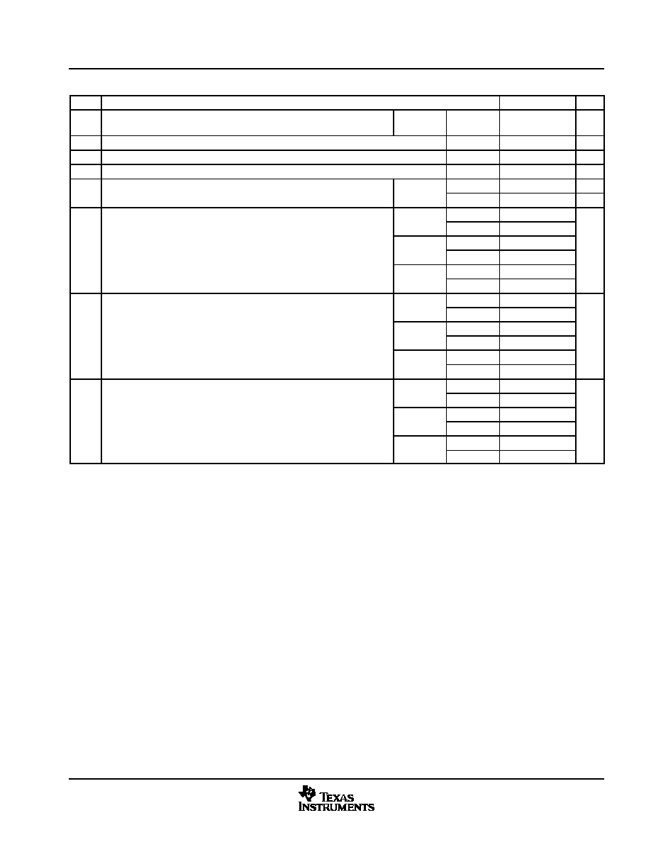
Electrical Specifications
143
August 2002 - Revised August 2004
SPRS197D
Table 5-15. McBSP Switching Characteristics
�
NO.
PARAMETER
MIN
MAX UNIT
M0
t
d(CKSH-CKRXH)
Delay time, CLKS high to CLKR/X high for internal
CLKR/X generated from CLKS input
McBSP1
CLKR/X int
2
33
ns
M1
t
c(CKRX)
Cycle time, CLKR/X
CLKR/X int
2P
ns
M2
t
w(CKRXH)
Pulse duration, CLKR/X high
CLKR/X int
0.45D
0.55D
ns
M3
t
w(CKRXL)
Pulse duration, CLKR/X low
CLKR/X int
0.45C
0.55C
ns
M4
t
Delay time CLKR high to internal FSR valid
McBSP2
CLKR int
-1
13
ns
M4
t
d(CKRH-FRV)
Delay time, CLKR high to internal FSR valid
McBSP2
CLKR ext
-3
24
ns
McBSP1
CLKX int
-4
13
McBSP1
CLKX ext
7
39
M5
t
Delay time CLKX high to internal FSX valid
McBSP2
CLKX int
-1
4
ns
M5
t
d(CKXH-FXV)
Delay time, CLKX high to internal FSX valid
McBSP2
CLKX ext
2
24
ns
McBSP3
CLKX int
-1
9
McBSP3
CLKX ext
2
37
McBSP1
CLKX int
-2
7
McBSP1
CLKX ext
7
40
M7
t
Delay time, CLKX high to DX valid.
This applies to all bits except the first bit transmitted McBSP2
CLKX int
0
10
ns
M7
t
d(CKXH-DXV)
This applies to all bits except the first bit transmitted
when in Data Delay 0 (XDATDLY=00b) mode.
McBSP2
CLKX ext
3
27
ns
when in Data Delay 0 (XDATDLY=00b) mode.
McBSP3
CLKX int
-1
10
McBSP3
CLKX ext
1
16
McBSP1
FSX int
28
�
McBSP1
FSX ext
25
M9
t
Delay time, FSX high to DX valid
�
O l
li fi bi
i d h i D
McBSP2
FSX int
30
ns
M9
t
d(FXH-DXV)
Only applies to first bit transmitted when in Data
Delay 0 (XDATDLY=00b) mode
McBSP2
FSX ext
27
ns
Delay 0 (XDATDLY=00b) mode.
McBSP3
FSX int
10
McBSP3
FSX ext
27
Polarity bits CLKRP = CLKXP = FSRP = FSXP = 0. If the polarity of any of the signals is inverted, then the timing references of
that signal are
also inverted.
P = 1/(Base frequency) for McBSP 1 and 3, or 1/(ARMPER_CK clock frequency) in ns for McBSP 2. Base frequency is 12 or 13 MHz.
�
T=CLKRX period = (1 + CLKGDV) * P
C=CLKRX low pulse width = T/2 when CLKGDV is odd or zero and = (CLKGDV/2) * P when CLKGDV is even
D=CLKRX high pulse width = T/2 when CLKGDV is odd or zero and = (CLKGDV/2 + 1) * P when CLKGDV is even
�
Only DXENA=0 is supported for all OMAP5910 McBSPs.
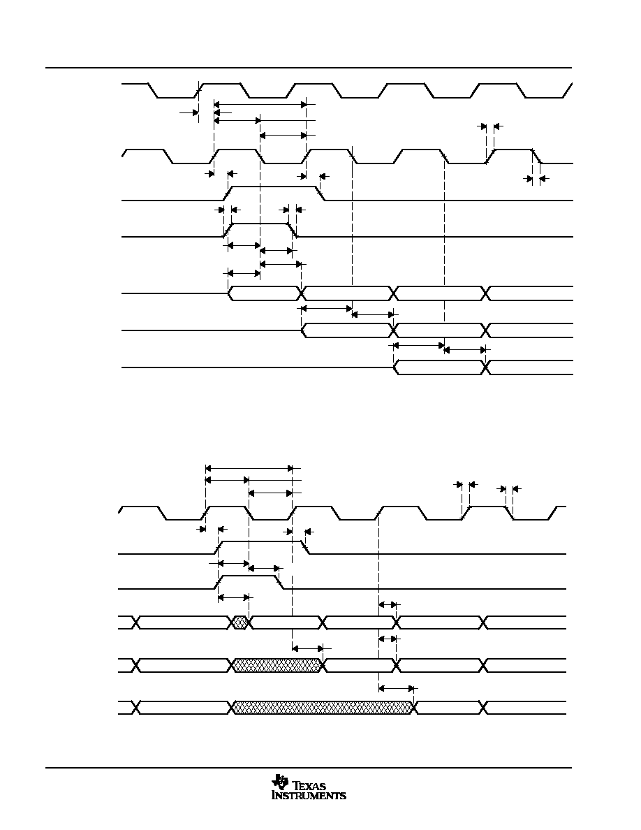
Electrical Specifications
144
August 2002 - Revised August 2004
SPRS197D
(n-2)
Bit (n-1)
(n-3)
(n-2)
Bit (n-1)
(n-4)
(n-3)
(n-2)
Bit (n-1)
M18
M17
M18
M17
M17
M18
M16
M15
M4
M4
M14
M13
M3, M12
M1, M11
M2, M12
(RDATDLY=10b)
MCBSPx.DR
(RDATDLY=01b)
MCBSPx.DR
(RDATDLY=00b)
MCBSPx.DR
MCBSPx.FSR/X
CBSP2.FSR (int)
CBSPx.CLKR/X
(ext)
M14
M13
MCBSP1.CLKS
M0
For McBSP1 and McBSP3, the receiver clock and frame sync inputs are driven by FSX and CLKX via internal loopback connections enabled
via software configuration. The M13 and M14 descriptors are applicable only to McBSP2.
Figure 5-18. McBSP Receive Timings
M7
M7
M7
M7
M9
(XDATDLY=10b)
MCBSPx.DX
(XDATDLY=01b)
MCBSPx.DX
(XDATDLY=00b)
MCBSPx.DX
(n-2)
Bit (n-1)
Bit 0
(n-4)
Bit (n-1)
(n-3)
(n-2)
Bit 0
(n-3)
(n-2)
Bit (n-1)
Bit 0
M20
M14
M13
M3, M12
M1, M11
M2, M12
MCBSPx.FSX
MCBSPx.FSX (int)
MCBSPx.CLKX
M5
M5
M19
(ext)
Figure 5-19. McBSP Transmit Timings

Electrical Specifications
145
August 2002 - Revised August 2004
SPRS197D
5.9.2 McBSP as SPI Master or Slave Timing
Table 5-16 to Table 5-23 assume testing over recommended operating conditions (see Figure 5-20 through
Figure 5-23).
Table 5-16. McBSP as SPI Master or Slave Timing Requirements (CLKSTP = 10b, CLKXP = 0)
NO
MASTER
SLAVE
UNIT
NO.
MIN
MAX
MIN
MAX
UNIT
M30
t
su(DRV-CKXL)
Setup time, MCBSPx.DR valid before MCBSPx.CLKX low
15
2 - 6P
ns
M31
t
h(CKXL-DRV)
Hold time, MCBSPx.DR valid after MCBSPx.CLKX low
2
6 + 6P
ns
S t ti
MCBSP FSX l
b f
McBSP1
21
M32
t
su(BFXL-CKXH)
Setup time, MCBSPx.FSX low before
MCBSPx.CLKX high
McBSP2
5
ns
su(BFXL CKXH)
MCBSPx.CLKX high
McBSP3
10
M33
t
c(CKX)
Cycle time, MCBSPx.CLKX
2P
16P
ns
For all SPI slave modes, CLKG is programmed as 1/2 of the internal reference clock by setting CLKSM = CLKGDV = 1.
P = 1/(Base frequency) for McBSP 1 and 3, or 1/(ARMPER_CK clock frequency) in ns for McBSP 2. Base frequency is 12 or 13 MHz.
Table 5-17. McBSP as SPI Master or Slave Switching Characteristics (CLKSTP = 10b, CLKXP = 0)
NO
PARAMETER
MASTER
�
SLAVE
UNIT
NO.
PARAMETER
MIN
MAX
MIN
MAX
UNIT
M24
t
h(CKXL-FXL)
Hold time, MCBSPx.FSX low after MCBSPx.CLKX low
�
0.45T
0.55T
ns
M25
t
d(FXL-CKXH)
Delay time, MCBSPx.FSX low to MCBSPx.CLKX high
#
0.45C
0.55C
ns
M26
t
d(CKXH-DXV)
Delay time, MCBSPx.CLKX high to MCBSPx.DX valid
-1
7
3P + 2
5P+ 18
ns
M29
t
d(FXL-DXV)
Delay time, MCBSPx.FSX low to MCBSPx.DX valid
4P + 18
ns
For all SPI slave modes, CLKG is programmed as 1/2 of the internal reference clock by setting CLKSM = CLKGDV = 1.
P = 1/(Base frequency) for McBSP 1 and 3, or 1/(ARMPER_CK clock frequency) in ns for McBSP 2. Base frequency is 12 or 13 MHz.
�
T = CLKX period = (1 + CLKGDV) * P
C = CLKX low pulse width = T/2 when CLKGDV is odd or zero and = (CLKGDV/2) * P when CLKGDV is even
�
FSRP = FSXP = 1. As a SPI master, MCBSPx.FSX is inverted to provide active-low slave-enable output. As a slave, the active-low signal input
on MCBSPx.FSX and MCBSPx.FSR is inverted before being used internally.
CLKXM = FSXM = 1, CLKRM = FSRM = 0 for master McBSP
CLKXM = CLKRM = FSXM = FSRM = 0 for slave McBSP
#
MCBSPx.FSX should be low before the rising edge of clock to enable slave devices and then begin a SPI transfer at the rising edge of the master
clock (MCBSPx.CLKX).
Bit 0
Bit(n-1)
(n-2)
(n-3)
(n-4)
Bit 0
Bit(n-1)
(n-2)
(n-3)
(n-4)
CLKX
FSX
DX
DR
M30
M26
M31
M24
M29
M25
LSB
MSB
M32
M33
Figure 5-20. McBSP Timing as SPI Master or Slave: CLKSTP = 10b, CLKXP = 0

Electrical Specifications
146
August 2002 - Revised August 2004
SPRS197D
Table 5-18. McBSP as SPI Master or Slave Timing Requirements (CLKSTP = 11b, CLKXP = 0)
NO
MASTER
SLAVE
UNIT
NO.
MIN
MAX
MIN
MAX
UNIT
M39
t
su(DRV-CKXH)
Setup time, MCBSPx.DR valid before MCBSPx.CLKX high
15
2 - 6P
ns
M40
t
h(CKXH-DRV)
Hold time, MCBSPx.DR valid after MCBSPx.CLKX high
2
6 +6P
ns
S t ti
MCBSP FSX l
b f
McBSP1
21
M41
t
su(FXL-CKXH)
Setup time, MCBSPx.FSX low before
MCBSPx.CLKX high
McBSP2
5
ns
su(FXL CKXH)
MCBSPx.CLKX high
McBSP3
10
M42
t
c(CKX)
Cycle time, MCBSPx.CLKX
2P
16P
ns
For all SPI slave modes, CLKG is programmed as 1/2 of the internal reference clock by setting CLKSM = CLKGDV = 1.
P = 1/(Base frequency) for McBSP 1 and 3, or 1/(ARMPER_CK clock frequency) in ns for McBSP 2. Base frequency is 12 or 13 MHz.
Table 5-19. McBSP as SPI Master or Slave Switching Characteristics (CLKSTP = 11b, CLKXP = 0)
NO
PARAMETER
MASTER
�
SLAVE
UNIT
NO.
PARAMETER
MIN
MAX
MIN
MAX
UNIT
M34
t
h(CKXL-FXL)
Hold time, MCBSPx.FSX low after MCBSPx.CLKX low
�
0.45C 0.55C
ns
M35
t
d(FXL-CKXH)
Delay time, MCBSPx.FSX low to MCBSPx.CLKX high
#
0.45T 0.55T
ns
M36
t
d(CKXL-DXV)
Delay time, MCBSPx.CLKX low to MCBSPx.DX valid
-1
7
3P + 2
5P + 18
ns
M38
t
d(FXL-DXV)
Delay time, MCBSPx.FSX low to MCBSPx.DX valid
D +20
4P + 18
ns
For all SPI slave modes, CLKG is programmed as 1/2 of the internal reference clock by setting CLKSM = CLKGDV = 1.
P = 1/(Base frequency) for McBSP 1 and 3, or 1/(ARMPER_CK clock frequency) in ns for McBSP 2. Base frequency is 12 or 13 MHz.
�
T = CLKX period = (1 + CLKGDV) * P
C = CLKX low pulse width = T/2 when CLKGDV is odd or zero and = (CLKGDV/2) * P when CLKGDV is even
D = CLKX high pulse width = T/2 when CLKGDV is odd or zero and = (CLKGDV/2 + 1) * P when CLKGDV is even
�
FSRP = FSXP = 1. As a SPI master, MCBSPx.FSX is inverted to provide active-low slave-enable output. As a slave, the active-low signal input
on MCBSPx.FSX and MCBSPx.FSR is inverted before being used internally.
CLKXM = FSXM = 1, CLKRM = FSRM = 0 for master McBSP
CLKXM = CLKRM = FSXM = FSRM = 0 for slave McBSP
#
MCBSPx.FSX should be low before the rising edge of clock to enable slave devices and then begin a SPI transfer at the rising edge of the master
clock (MCBSPx.CLKX).
Bit 0
Bit(n-1)
(n-2)
(n-3)
(n-4)
Bit 0
Bit(n-1)
(n-2)
(n-3)
(n-4)
MCBSPx.CLKX
MCBSPx.FSX
MCBSPx.DX
MCBSPx.DR
M35
M36
M40
M39
M38
M34
LSB
MSB
M41
M42
Figure 5-21. McBSP Timing as SPI Master or Slave: CLKSTP = 11b, CLKXP = 0

Electrical Specifications
147
August 2002 - Revised August 2004
SPRS197D
Table 5-20. McBSP as SPI Master or Slave Timing Requirements (CLKSTP = 10b, CLKXP = 1)
NO
MIN
MASTER
SLAVE
UNIT
NO.
MIN
MIN
MAX
MIN
MAX
UNIT
M49
t
su(DRV-CKXH)
Setup time, MCBSPx.DR valid before MCBSPx.CLKX high
15
2 - 2P
ns
M50
t
h(CKXH-DRV)
Hold time, MCBSPx.DR valid after MCBSPx.CLKX high
2
6 + 6P
ns
S t ti
MCBSP FSX l
b f
McBSP1
21
M51
t
su(FXL-CKXL)
Setup time, MCBSPx.FSX low before
MCBSPx.CLKX low
McBSP2
5
ns
su(FXL CKXL)
MCBSPx.CLKX low
McBSP3
10
M52
t
c(CKX)
Cycle time, MCBSPx.CLKX
2P
16P
ns
For all SPI slave modes, CLKG is programmed as 1/2 of the CPU clock by setting CLKSM = CLKGDV = 1.
P = 1/(Base frequency) for McBSP 1 and 3, or 1/(ARMPER_CK clock frequency) in ns for McBSP 2. Base frequency is 12 or 13 MHz.
Table 5-21. McBSP as SPI Master or Slave Switching Characteristics (CLKSTP = 10b, CLKXP = 1)
NO
PARAMETER
MASTER
�
SLAVE
UNIT
NO.
PARAMETER
MIN
MAX
MIN
MAX
UNIT
M43
t
h(CKXH-FXL)
Hold time, MCBSPx.FSX low after MCBSPx.CLKX high
�
0.45T 0.55T
ns
M44
t
d(FXL-CKXL)
Delay time, MCBSPx.FSX low to MCBSPx.CLKX low
#
0.45D 0.55D
ns
M45
t
d(CKXL-DXV)
Delay time, MCBSPx.CLKX low to MCBSPx.DX valid
-1
7
3P + 2
5P + 18
ns
M48
t
d(FXL-DXV)
Delay time, MCBSPx.FSX low to MCBSPx.DX valid
4P + 18
ns
For all SPI slave modes, CLKG is programmed as 1/2 of the internal reference clock by setting CLKSM = CLKGDV = 1.
P = 1/(Base frequency) for McBSP 1 and 3, or 1/(ARMPER_CK clock frequency) in ns for McBSP 2. Base frequency is 12 or 13 MHz.
�
T = CLKX period = (1 + CLKGDV) * P
D = CLKX high pulse width = T/2 when CLKGDV is odd or zero and = (CLKGDV/2 + 1) * P when CLKGDV is even
�
FSRP = FSXP = 1. As a SPI master, MCBSPx.FSX is inverted to provide active-low slave-enable output. As a slave, the active-low signal input
on MCBSPx.FSX and MCBSPx.FSR is inverted before being used internally.
CLKXM = FSXM = 1, CLKRM = FSRM = 0 for master McBSP
CLKXM = CLKRM = FSXM = FSRM = 0 for slave McBSP
#
MCBSPx.FSX should be low before the rising edge of clock to enable slave devices and then begin a SPI transfer at the rising edge of the master
clock (MCBSPx.CLKX).
M51
M50
Bit 0
Bit(n-1)
(n-2)
(n-3)
(n-4)
Bit 0
Bit(n-1)
(n-2)
(n-3)
(n-4)
MCBSPx.CLKX
MCBSPx.FSX
MCBSPx.DX
MCBSPx.DR
M44
M48
M45
M49
M43
LSB
M52
MSB
Figure 5-22. McBSP Timing as SPI Master or Slave: CLKSTP = 10b, CLKXP = 1
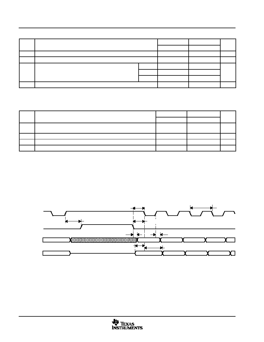
Electrical Specifications
148
August 2002 - Revised August 2004
SPRS197D
Table 5-22. McBSP as SPI Master or Slave Timing Requirements (CLKSTP = 11b, CLKXP = 1)
NO
MIN
MASTER
SLAVE
UNIT
NO.
MIN
MIN
MAX
MIN
MAX
UNIT
M58
t
su(DRV-CKXL)
Setup time, MCBSPx.DR valid before MCBSPx.CLKX low
15
2 - 6P
ns
M59
t
h(CKXL-DRV)
Hold time, MCBSPx.DR valid after MCBSPx.CLKX low
2
6 + 6P
ns
S t ti
MCBSP FSX l
b f
McBSP1
21
M60
t
su(FXL-CKXL)
Setup time, MCBSPx.FSX low before
MCBSPx.CLKX low
McBSP2
5
ns
su(FXL CKXL)
MCBSPx.CLKX low
McBSP3
10
M61
t
c(CKX)
Cycle time, MCBSPx.CLKX
2P
16P
ns
For all SPI slave modes, CLKG is programmed as 1/2 of the internal reference clock by setting CLKSM = CLKGDV = 1.
P = 1/(Base frequency) for McBSP 1 and 3, or 1/(ARMPER_CK clock frequency) in ns for McBSP 2. Base frequency is 12 or 13 MHz.
Table 5-23. McBSP as SPI Master or Slave Switching Characteristics (CLKSTP = 11b, CLKXP = 1)
NO
PARAMETER
MASTER
�
SLAVE
UNIT
NO.
PARAMETER
MIN
MAX
MIN
MAX
UNIT
M53
t
h(CKXH-FXL)
Hold time, MCBSPx.FSX low after MCBSPx.CLKX
high
�
0.45D
0.55D
ns
M54
t
d(FXL-CKXL)
Delay time, MCBSPx.FSX low to MCBSPx.CLKX low
#
0.45T
0.55T
ns
M55
t
d(CKXH-DXV)
Delay time, MCBSPx.CLKX high to MCBSPx.DX valid
-1
7
3P + 2
5P + 18
ns
M57
t
d(FXL-DXV)
Delay time, MCBSPx.FSX low to MCBSPx.DX valid
C + 20
4P + 18
ns
For all SPI slave modes, CLKG is programmed as 1/2 of the internal reference clock by setting CLKSM = CLKGDV = 1.
P = 1/(Base frequency) for McBSP 1 and 3, or 1/(ARMPER_CK clock frequency) in ns for McBSP 2. Base frequency is 12 or 13 MHz.
�
T = CLKX period = (1 + CLKGDV) * P
C = CLKX low pulse width = T/2 when CLKGDV is odd or zero and = (CLKGDV/2) * P when CLKGDV is even
D = CLKX high pulse width = T/2 when CLKGDV is odd or zero and = (CLKGDV/2 + 1) * P when CLKGDV is even
�
FSRP = FSXP = 1. As a SPI master, MCBSPx.FSX is inverted to provide active-low slave-enable output. As a slave, the active-low signal input
on MCBSPx.FSX and MCBSPx.FSR is inverted before being used internally.
CLKXM = FSXM = 1, CLKRM = FSRM = 0 for master McBSP
CLKXM = CLKRM = FSXM = FSRM = 0 for slave McBSP
#
MCBSPx.FSX should be low before the rising edge of clock to enable slave devices and then begin a SPI transfer at the rising edge of the master
clock (MCBSPx.CLKX).
Bit 0
Bit(n-1)
(n-2)
(n-3)
(n-4)
Bit 0
Bit(n-1)
(n-2)
(n-3)
(n-4)
MCBSPx.CLKX
MCBSPx.FSX
MCBSPx.DX
MCBSPx.DR
M54
M58
M53
M55
M59
M57
LSB
MSB
M60
M61
Figure 5-23. McBSP Timing as SPI Master or Slave: CLKSTP = 11b, CLKXP = 1

Electrical Specifications
149
August 2002 - Revised August 2004
SPRS197D
5.10 Multichannel Serial Interface (MCSI)
Table 5-24 and Table 5-25 assume testing over recommended operating conditions (see Figure 5-24 and
Figure 5-25).
Table 5-24. MCSI Timing Requirements
NO.
MIN
MAX
UNIT
MC11 f
op(CLK)
Operating frequency, MCSIx.CLK
Slave
B
MHz
MC12 t
w(CLKH)
Pulse duration, MCSIx.CLK high
Slave
0.45P
0.55P
ns
MC13 t
w(CLKL)
Pulse duration, MCSIx.CLK low
Slave
0.45P
0.55P
ns
MC14 t
r(CLK)
Rise time, MCSIx.CLK
Slave
12
ns
MC15 t
f(CLK)
Fall time, MCSIx.CLK
Slave
12
ns
MC16 t
Setup time external MCSIx SYNC high before MCSIx CLK low Slave
18
ns
MC16 t
su(FSH-CLKL)
Setup time, external MCSIx.SYNC high before MCSIx.CLK low Slave
18
ns
MC17 t
Hold time external MCSIx SYNC high after MCSIx CLK low
Slave
6
ns
MC17 t
h(CLKL-FSH)
Hold time, external MCSIx.SYNC high after MCSIx.CLK low
Slave
6
ns
MC18 t
Setup time MCSIx DIN valid before MCSIx CLK low
Master
27
ns
MC18 t
su(DIV-CLKL)
Setup time, MCSIx.DIN valid before MCSIx.CLK low
Slave
18
ns
MC19 t
Hold time MCSIx DIN valid after MCSIx CLK low
Master
0
ns
MC19 t
h(CLKL-DIV)
Hold time, MCSIx.DIN valid after MCSIx.CLK low
Slave
6
ns
P = MCSIx.CLK period [t
c(CLK)
] in nanoseconds.
B = Base frequency for OMAP5910 (12 or 13 MHz).
Table 5-25. MCSI Switching Characteristics
NO.
PARAMETER
MIN
MAX UNIT
MC1
f
op(CLK)
Operating frequency, MCSIx.CLK
Master
0.5B
MHz
MC2
t
w(CLKH)
Pulse duration, MCSIx.CLK high
Master
0.45P
0.55P
ns
MC3
t
w(CLKL)
Pulse duration, MCSIx.CLK low
Master
0.45P
0.55P
ns
MC4
t
Delay time MCSIx CLK high to MCSIx SYNC transition
Master
0
5
ns
MC4
t
d(CLKH-FS)
Delay time, MCSIx.CLK high to MCSIx.SYNC transition
Master
0
5
ns
MC7
t
Delay time MCSIx CLK high to MCSIx DOUT valid
Master
0
5
ns
MC7
t
d(CLKH-DOV)
Delay time, MCSIx.CLK high to MCSIx.DOUT valid
Slave
2
30
ns
MC8
t
Enable time MCSIx DOUT driven from MCSIx CLK high
Master
0
ns
MC8
t
en(CLKH-DO)
Enable time, MCSIx.DOUT driven from MCSIx.CLK high
Slave
2
ns
P = MCSIx.CLK period [t
c(CLK)
] in nanoseconds.
B = Base frequency for OMAP5910 (12 or 13 MHz).
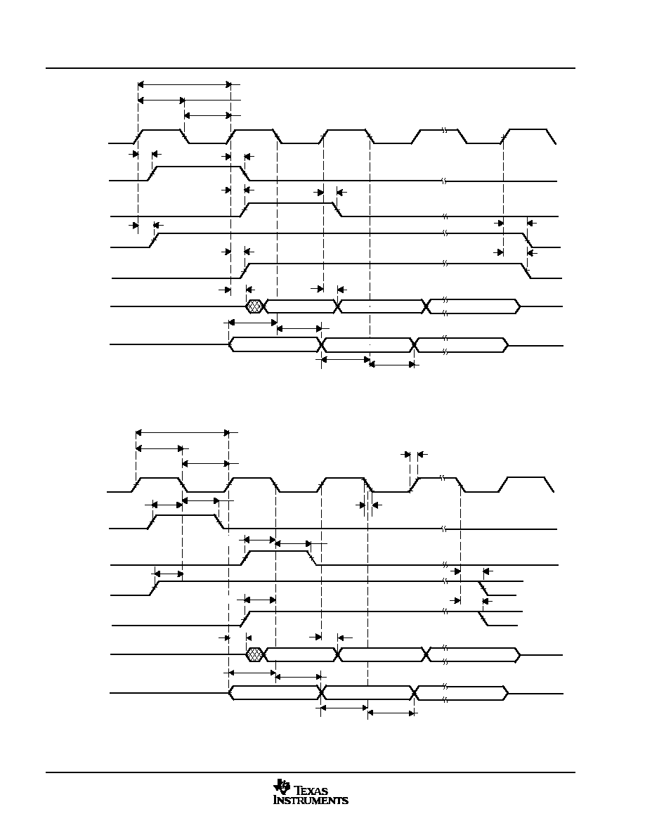
Electrical Specifications
150
August 2002 - Revised August 2004
SPRS197D
Bit (n)
MC19
MC19
MC18
MC4
MC4
MC3
1/MC1
MC2
MCSIx.DIN
MCSIx.SYNC
MCSIx.CLK
MC7
MC8
MCSIx.DOUT
Bit (n)
MC4
MC4
MCSIx.SYNC
(normal short)
(alt. short)
MC4
MC4
MCSIx.SYNC
(normal long)
MCSIx.SYNC
(alt. long)
(0)
(0)
MC4
MC4
MC18
(n-1)
(n-1)
Figure 5-24. MCSI Master Mode Timings
(n-1)
Bit (n)
MC19
MC19
MC18
MC16
MC15
MC14
MC13
1/MC11
MC12
MCSIx.DIN
MCSIx.SYNC
MCSIx.CLK
MC7
MC8
MCSIx.DOUT
(n-1)
Bit (n)
MCSIx.SYNC
(normal short)
(alt. short)
MC17
MCSIx.SYNC
(normal long)
MCSIx.SYNC
(alt. long)
(0)
(0)
M17
MC16
MC17
MC16
MC16
MC18
MC17
Figure 5-25. MCSI Slave Mode Timings
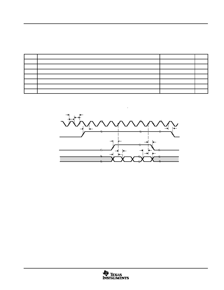
Electrical Specifications
151
August 2002 - Revised August 2004
SPRS197D
5.11 Camera Interface Timings
Table 5-26 assumes testing over recommended operating conditions (see Figure 5-26).
Table 5-26. Camera Interface Timing Requirements
NO.
MIN
MAX
UNIT
C1
1 / [ t
c(LCKH-HSV)
]
Operating frequency, CAM.LCLK
13
MHz
C2
1 / [ t
c(XCKH-HSV)
]
Operating frequency, CAM.EXCLK
24
MHz
C3
t
w(LCK)
Pulse duration, CAM.LCLK high or low
0.45P
0.55P
ns
C5
t
su(LCKH-DV)
Setup time, CAM.D[7:0] data valid before CAM.LCLK high
1
ns
C6
t
h(DV-LCKH)
Hold time, CAM.D[7:0] data valid after CAM.LCLK high
9
ns
C7
t
su(LCKH-DV)
Setup time, CAM.VS/CAM.HS active before CAM.LCLK high
1
ns
C8
t
h(DV-CLKH)
Hold time, CAM.VS/CAM.HS active after CAM.LCLK high
9
ns
P = period of CAM.LCLK in nanoseconds (ns).
Polarity of CAM.LCLK is selectable via the POLCLK bit in the CTRLCLOCK register. Although data is latched on rising CAM.LCLK in the timing
diagrams, these timing parameters also apply to falling CAM.LCLK when POLCLK = 1.
CAM.LCLK
CAM.HS
CAM.D[7:0]
CAM.VS
U1
Y1
V1
Yn
C7
C6
C7
C8
C8
C5
C6
C5
C3
C3
C1
Figure 5-26. Camera Interface Timings
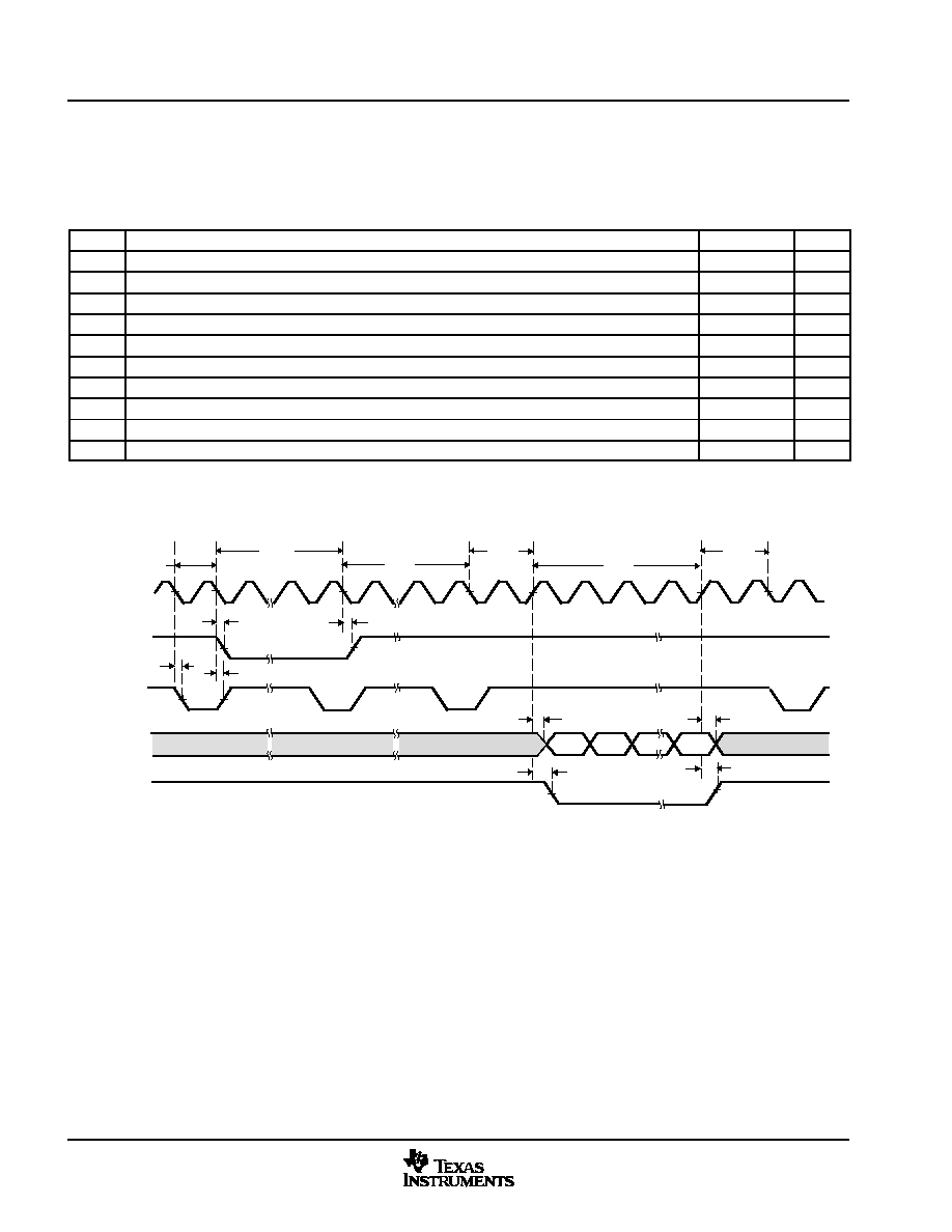
Electrical Specifications
152
August 2002 - Revised August 2004
SPRS197D
5.12 LCD Controller Timings
Table 5-27 assumes testing over recommended operating conditions (see Figure 5-27 and Figure 5-28).
Table 5-27. LCD Controller Switching Characteristics
NO.
PARAMETER
MIN
MAX
UNIT
L1
t
d(CLKH-HSV)
Delay time, LCD.PCLK high to LCD.HS transition
1
11
ns
L2
t
d(CLKL-HSV)
Delay time, LCD.PCLK low to LCD.HS transition
1
11
ns
L3
t
d(CLKH-VSV)
Delay time, LCD.PCLK high to LCD.VS transition
1
11
ns
L4
t
d(CLKL-VSV)
Delay time, LCD.PCLK low to LCD.VS transition
1
11
ns
L5
t
d(CLKH-PV)
Delay time, LCD.PCLK high to pixel data valid (LCD.P[15:0])
11
ns
L6
t
d(CLKH-PIV)
Delay time, LCD.PCLK high to pixel data invalid (LCD.P[15:0])
1
ns
L7
t
d(CLKL-PV)
Delay time, LCD.PCLK low to pixel data valid (LCD.P[15:0])
11
ns
L8
t
d(CLKL-PIV)
Delay time, LCD.PCLK low to pixel data invalid (LCD.P[15:0])
1
ns
L9
t
d(CLKL-ACV)
Delay time, LCD.PCLK high to LCD.AC transition
1
5+P
ns
L10
t
d(CLKL-ACV)
Delay time, LCD.PCLK low to LCD.AC transition
1
5+P
ns
Although timing diagrams illustrate the logical function of the TFT mode, static timings apply to all supported modes of operation. Likewise,
LCD.HS, LCD.VS, and LCD.AC are shown as active-low, but each may optionally be configured as active-high.
P = period of internal undivided pixel clock
LCD.PCLK
LCD.VS
LCD.P[15:0]
LCD.AC
LCD.HS
L4
L9
L5
D1
D2
D3
Dn
L6
L9
L4
L2
L2
HSW
VSW
VFP
HFP
HBP
PPL
Delays for HSW (LCD.HS Width), VSW (LCD.VS Width), VFP (Vertical Front Porch), HFP (Horizontal Front Porch), HBP (Horizontal Back Porch)
and PPL (Pixels per Line) are programmable in number of LCD.PCLK cycles via the LCD configuration registers.
Figure 5-27. TFT Mode (LCD.HS/LCD.VS on Falling and LCD.Px on Rising LCD.PCLK)
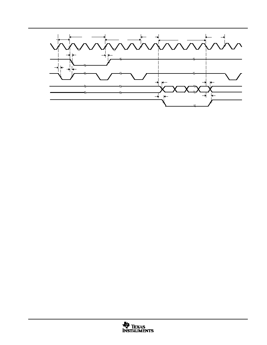
Electrical Specifications
153
August 2002 - Revised August 2004
SPRS197D
LCD.PCLK
LCD.VS
LCD.P[15:0]
LCD.AC
LCD.HS
L3
L7
D1
D2
D3
Dn
L8
L3
L1
L1
HSW
HBP
PPL
L10
L10
VSW
VFP
HFP
Delays for HSW (LCD.HS Width), VSW (LCD.VS Width), VFP (Vertical Front Porch), HFP (Horizontal Front Porch), HBP (Horizontal Back Porch)
and PPL (Pixels per Line) are programmable in number of LCD.PCLK cycles via the LCD configuration registers.
Figure 5-28. TFT Mode (LCD.HS/LCD.VS on Rising and LCD.Px on Falling LCD.PCLK)

Electrical Specifications
154
August 2002 - Revised August 2004
SPRS197D
5.13 Multimedia Card/Secure Digital (MMC/SD) Timings
Table 5-28 and Table 5-29 assume testing over recommended operating conditions (see Figure 5-29
through Figure 5-32).
Table 5-28. MMC/SD Timing Requirements
NO.
MIN
MAX
UNIT
M1
t
su(CMDV-CLKH)
Setup time, MMC.CMD valid before MMC.CLK high
12
ns
M2
t
h(CLKH-CMDV)
Hold time, MMC.CMD invalid after MMC.CLK high
2
ns
M3
t
su(DATV-CLKH)
Setup time, MMC.DATx valid before MMC.CLK high
12
ns
M4
t
h(CLKH-DATV)
Hold time, MMC.DATx invalid after MMC.CLK high
2
ns
Table 5-29. MMC/SD Switching Characteristics
NO.
PARAMETER
MIN
MAX
UNIT
M7
t
Cycle time MMC CLK
41.7
ns
M7
t
c(CLK)
Cycle time, MMC.CLK
5.31
us
M8
t
w(CLKH)
Pulse Duration, MMC.CLK high
20
ns
M9
t
w(CLKL)
Pulse Duration, MMC.CLK low
20
ns
M10
t
d(CLKH-CMD)
Delay time, MMC.CLK high to MMC.CMD transition
4
48
ns
M11
t
d(CLKH-DAT)
Delay time, MMC.CLK high to MMC.DATx transition
4
48
ns
MMC.CLK period and pulse duration depends upon software configuration.
MMC.CLK
MMC.CMD
XMIT
Valid
M10
M10
M10
M10
Valid
Valid
Start
End
M9
M8
M7
Figure 5-29. MMC/SD Host Command Timings
MMC.CLK
MMC.CMD
M7
XMIT
Valid
Valid
Valid
Start
End
M1
M1
M2
M9
M8
M2
Figure 5-30. MMC/SD Card Response Timings

Electrical Specifications
155
August 2002 - Revised August 2004
SPRS197D
MMC.CLK
MMC.DATx
M11
M11
M11
M11
End
Start
D0
D1
D2
Dx
M9
M8
M7
Figure 5-31. MMC/SD Host Write Timings
MMC.CLK
MMC.DATx
M4
M3
End
Start
D0
D1
D2
Dx
M3
M4
M7
M9
M8
Figure 5-32. MMC/SD Host Read and Card CRC Status Timings

Electrical Specifications
156
August 2002 - Revised August 2004
SPRS197D
5.14 I
2
C Timings
Table 5-30 assumes testing over recommended operating conditions (see Figure 5-33).
Table 5-30. I
2
C Signals (I2C.SDA and I2C.SCL) Switching Characteristics
NO.
PARAMETER
STANDARD
MODE
FAST
MODE
UNIT
NO.
PARAMETER
MIN
MAX
MIN
MAX
UNIT
IC1
t
c(SCL)
Cycle time, I2C.SCL
10
2.5
�s
IC2
t
su(SCLH-SDAL)
Setup time, I2C.SCL high before I2C.SDA low (for a repeated START
condition)
4.7
0.6
�s
IC3
t
h(SCLL-SDAL)
Hold time, I2C.SCL low after I2C.SDA low (for a repeated START
condition)
4
0.6
�s
IC4
t
w(SCLL)
Pulse duration, I2C.SCL low
4.7
1.3
�s
IC5
t
w(SCLH)
Pulse duration, I2C.SCL high
4
0.6
�s
IC6
t
su(SDA-SDLH)
Setup time, I2C.SDA valid before I2C.SCL high
250
100
ns
IC7
t
h(SDA-SDLL)
Hold time, I2C.SDA valid after I2C.SCL low (for I
2
C bus devices)
0
0
0.9
�s
IC8
t
w(SDAH)
Pulse duration, I2C.SDA high between STOP and START conditions
4.7
1.3
�s
IC9
t
r(SDA)
Rise time, I2C.SDA
1000
300
ns
IC10
t
r(SCL)
Rise time, I2C.SCL
1000
300
ns
IC11
t
f(SDA)
Fall time, I2C.SDA
300
300
ns
IC12
t
f(SCL)
Fall time, I2C.SCL
300
300
ns
IC13
t
su(SCLH-SDAH)
Setup time, I2C.SCL high before I2C.SDA high (for STOP condition)
4.0
0.6
�s
IC14
t
w(SP)
Pulse duration, spike (must be suppressed)
0
50
ns
IC15
C
b
�
Capacitive load for each bus line
400
400
pF
In the master-only I
2
C operating mode of OMAP5910, minimum cycle time for I2C.SCL is 12 �s.
The maximum t
h(SCLL-SDAL)
has only to be met if the device does not stretch the low period (t
w(SCLL)
) of the I2C.SCL signal.
�
C
b
= The total capacitance of one bus line in pF.
IC10
IC8
IC4
IC3
IC7
IC12
IC5
IC6
IC14
IC2
IC3
IC13
Stop
Start
Repeated
Start
Stop
I2C.SDA
I2C.SCL
IC1
NOTES: A. A device must internally provide a hold time of at least 300 ns for the I2C.SDA signal (referred to the V
IHmin
of the I2C.SCL signal
)
to bridge the undefined region of the falling edge of I2C.SCL.
B. The maximum t
h(SCLL-SDAL)
has only to be met if the device does not stretch the LOW period (t
w(SCLL)
) of the I2C.SCL signal.
C. A Fast-mode I
2
C-bus device can be used in a standard-mode I
2
C-bus system, but the requirement t
su(SDA-SDLH)
� 250 ns must then
be met. This is automatically the case if the device does not stretch the LOW period of the I2C.SCL signal. If such a device does
stretch the LOW period of the I2C.SCL signal, it must output the next data bit to the I2C.SDA line t
r
max + t
su(SDA-SDLH)
=
1000 + 250 = 1250 ns (according to the standard-mode I
2
C-bus specification) before the I2C.SCL line is released.
D. C
b
= total capacitance of one bus line in pF. If mixed with fast-mode devices, faster fall times are allowed.
Figure 5-33. I
2
C Timings
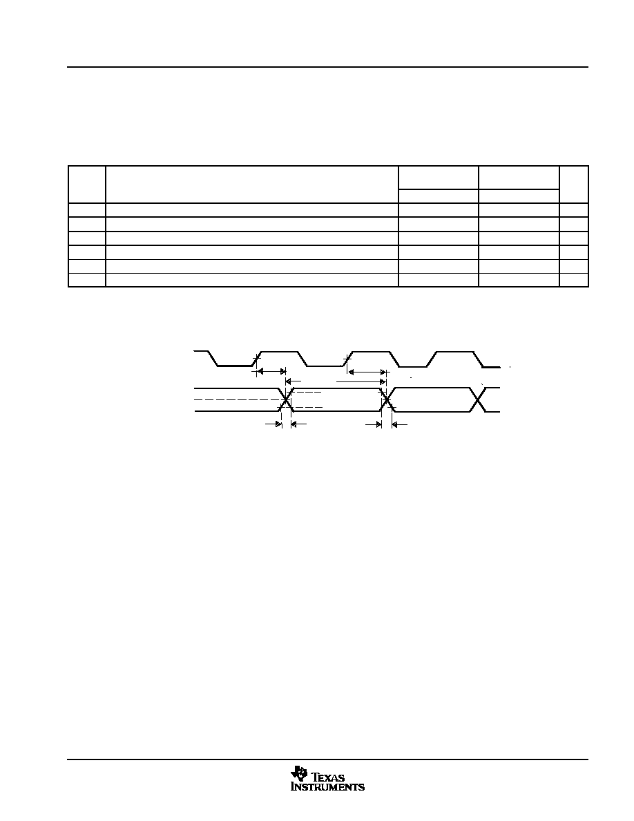
Electrical Specifications
157
August 2002 - Revised August 2004
SPRS197D
5.15 Universal Serial Bus (USB) Timings
All OMAP5910 USB interfaces are compliant with the Universal Serial Bus Specification, Revision 2.0.
Table 5-31 assumes testing over recommended operating conditions (see Figure 5-34).
Table 5-31. USB Integrated Transceiver Interface Switching Characteristics
NO.
PARAMETER
LOW SPEED
1.5 Mbps
FULL SPEED
12 Mbps
UNIT
NO.
PARAMETER
MIN
MAX
MIN
MAX
UNIT
U1
t
r
Rise time, USB.DP and USB.DM signals
75
300
4
20
ns
U2
t
f
Fall time, USB.DP and USB.DM signals
75
300
4
20
ns
U3
t
RFM
Rise/Fall time matching
80
125
90
111.11
%
U4
V
CRS
Output signal cross-over voltage
1.3
2.0
1.3
2.0
V
U5
t
jr
Differential propagation jitter
�
-25
�
25
�
-2
�
2
�
ns
U6
f
op
Operating frequency
�
1.5
12
MHz
Low Speed: C
L
= 200 pF, Full Speed: C
L
= 50 pF
t
RFM =
(t
r
/t
f
) x 100
�
t
jr =
t
px(1)
- t
px(0)
�
f
op =
1/t
per
V
OL
U1
U2
V
CRS
V
OH
90%
10%
REF clock
USB.DM
USB.DP
t
px(0)
t
px(1)
t
per -
t
jr
"REF clock" is not an actual device signal, but an ideal reference clock against which relative timings are specified. REF clock is assumed to be
12 MHz for full-speed mode or 1.5 MHz for low-speed mode).
Figure 5-34. USB Integrated Transceiver Interface Timings

Electrical Specifications
158
August 2002 - Revised August 2004
SPRS197D
5.16 MICROWIRE Interface Timings
Table 5-32 and Table 5-33 assume testing over recommended operating conditions (see Figure 5-35).
Table 5-32. MICROWIRE Timing Requirements
NO.
MIN
MAX
UNIT
W5
t
su(SDI-SCLK)
Setup time, UWIRE.SDI valid before UWIRE.SCLK active edge
21
ns
W6
t
h(SCLK-SDI)
Hold time, UWIRE.SDI invalid after UWIRE.SCLK active edge
6
ns
Polarity of UWIRE.SCLK and the active clock edge (rising or falling) on which SDO data is driven and SDI data is latched is all software
configurable. These timings apply to all configurations regardless of UWIRE.SCLK polarity and which clock edges are used to drive output data
and capture input data.
Table 5-33. MICROWIRE Switching Characteristics
NO.
PARAMETER
MIN
MAX
UNIT
W1
f
op(SCLK)
Operating Frequency, UWIRE.SCLK
3
MHz
W2
t
w(SCLK)
Pulse Duration, UWIRE.SCLK high/low
0.45P
0.55P
ns
W3
t
d(SCLK-SDO)
Delay time, UWIRE.SCLK active edge to UWIRE.SDO transition
-3
6
ns
W4
t
d(CS-SCLK)
Delay time, UWIRE.CSx active to UWIRE.SCLK active
1.5P
ns
Polarity of UWIRE.SCLK and the active clock edge (rising or falling) on which SDO data is driven and SDI data is latched is all software
configurable. These timings apply to all configurations regardless of UWIRE.SCLK polarity and which clock edges are used to drive output data
and capture input data.
P = UWIRE.SCLK cycle time in ns.
UWIRE.SCLK
UWIRE.CSx
W2
W2
UWIRE.SDO
W3
[1/W1]
UWIRE.SDI
Valid
Valid
Valid
Valid
Valid
Valid
W3
W5
W6
W4
W4
NOTE: The polarities of UWIRE.CSx and UWIRE.SCLK and the active UWIRE.SCLK edges on which SDO is driven and SDI is sampled are all
software configurable.
Figure 5-35. MICROWIRE Timings
Electrical Specifications
159
August 2002 - Revised August 2004
SPRS197D
5.17 HDQ/1-Wire Interface Timings
Table 5-34 and Table 5-35 assume testing over recommended operating conditions (see Figure 5-36
through Figure 5-39).
Table 5-34. HDQ/1-Wire Timing Requirements
MIN
MAX
UNIT
H1
t
c
Cycle time, master read
190
250
�s
H2
t
v
Read one data valid after HDQ low
32
50
�s
H3
t
v
Read zero data hold after HDQ low
80
145
�s
H4
t
Response time from HDQ slave device
OMAP5910 base
frequency = 12 MHz
190
320
�s
H4
t
v
Response time from HDQ slave device
OMAP5910 base
frequency = 13 MHz
190
303
�s
W1
t
c
Cycle time, master read
190
�s
W2
t
v
Read data valid after HDQ low (master sample window)
12
13.6
�s
W3
t
dis
Recovery time after slave device inactive
1
�s
HDQ timing is OMAP5910 default. 1-Wire timing is selectable through software.
Table 5-35. HDQ/1-Wire Switching Characteristics
PARAMETER
MIN
MAX
UNIT
H5
t
c
Cycle time, master write
190
�s
H6
t
d
Write one data valid after HDQ low
32
50
�s
H7
t
Write zero data hold after HDQ low
OMAP5910 base
frequency = 12 MHz
100
145
�s
H7
t
d
Write zero data hold after HDQ low
OMAP5910 base
frequency = 13 MHz
92
145
�s
H8
t
w
Pulse width, HDQ low for break pulse (reset)
190
�s
H9
t
w
Pulse width, HDQ high for break pulse recovery
40
�s
W4
t
c
Cycle time, master write
190
�s
W5
t
d
Write zero master inactive after HDQ low
15
90
�s
W6
t
d
Write one master inactive after HDQ low
1.1
1.4
�s
W7
t
dis
Recovery time after master inactive
1
�s
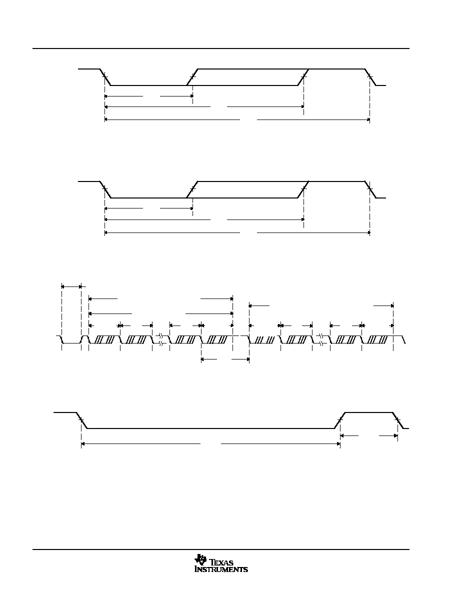
Electrical Specifications
160
August 2002 - Revised August 2004
SPRS197D
HDQ
H2
H3
H1
Read 0
Read 1
Figure 5-36. OMAP5910 HDQ Interface Reading From HDQ Slave Device
HDQ
H6
H7
H5
Write 0
Write 1
Figure 5-37. OMAP5910 HDQ Interface Writing to HDQ Slave Device
Break
1
6
Register Address
Command Byte
(Written by OMAP5910)
1
6
Data Byte
(Received by OMAP5910 from Slave)
H4
HDQ
0
(LSB)
7
(MSB)
7
(MSB)
0
(LSB)
Figure 5-38. Typical Communication Between OMAP5910 HDQ and HDQ Slave
H11
H12
HDQ
H8
H9
HDQ
Figure 5-39. HDQ/1-Wire Break (Reset) Timing

Glossary
161
August 2002 - Revised August 2004
SPRS197D
6
Glossary
ACRONYM
DEFINITION
1-wire
a serial protocol defined by Dallas Semiconductor Corporation
AAC
Advanced Audio Coding (standard) (ISO/IEC 13818-7)
AC97
Interface Standard for Codecs
ALU
arithmetic/logic unit
AMR
Adaptive Multi-Rate
ASRAM
asynchronous static RAM
AU
address unit
BCD
binary coded decimal
BGA
ball grid array
CMOS
complementary metal oxide semiconductor
CP15
coprocessor 15
CRC
cyclic redundancy check
CSL
Chip Support Library
CTS
clear-to-send
DARAM
dual-access RAM
DCT
discrete cosine transform
DMA
direct memory access
DPLL
digital phase-locked loop
DSP
digital signal processor
DSPLIB
DSP Library
DSR
data-set-ready
DTR
data-terminal-ready
DU
data unit
EMIFF
external memory interface fast
EMIFS
external memory interface slow
EP
endpoint
ESD
electrostatic discharge
ETM
FAC
frame adjustment counter
FFT
Fast Fourier Transform
FIFO
first-in first out
FIQ
fast interrupt request
GPRS
General Packet Radio Service
GSM
Global System for Mobile Communications
H.26x
an ITU-TSS standard
HBM
Human Body Model
HBP
Horizontal Back Porch

Glossary
162
August 2002 - Revised August 2004
SPRS197D
DEFINITION
ACRONYM
HDQ
a single-wire serial interface protocol defined by Benchmarq Controls Inc.
HFP
Horizontal Front Porch
HOM
host-only mode
HS
high-speed
I-cache
instruction cache
I
2
C
Inter-integrated circuit
I
2
S
Inter-IC Sound (specification)
iDCT
Inverse Discrete Cosine Transform
I/F
interface
IFR
Interrupt Flag Register
IMGLIB
Image/Video Processing Library
IMIF
internal memory interface
IMR
Interrupt Mask Register
IOM-2
ISDN Oriented Modular Interface Revision 2
IrDA
infrared data adapter
IRQ
low-priority interrupt request
IU
instruction unit
JPEG
Joint Photographic Experts Group - standard for compressed still-picture data
LB
local bus
LCD
liquid crystal display
LPG
LED pulse generator
LSB
least significant bit
LVCMOS
low-voltage CMOS
MAC
multiply-accumulate
MCSI
multichannel serial interface
McBSP
multichannel buffered serial port
MMC
multimedia card
MMC/SD
multimedia card/secure digital
MMU
memory management unit
MPEG
Moving Picture Experts Group - proposed standard for compressed video data
MPU
microprocessor unit
MPUI
microprocessor unit interface
MPUIO
microprocessor unit I/O
MSB
most significant bit
MVIP
multi-vendor integration protocol
ODM
original design manufacturer
OEM
original equipment manufacturer
OHCI
Open Host Controller Interface
OS
operating system
Benchmarq is a trademark of Texas Instruments.

Glossary
163
August 2002 - Revised August 2004
SPRS197D
DEFINITION
ACRONYM
PPL
pixels per line
PU
program unit
PWL
pulse-width light
PWT
pulse-width tone
RISC
reduced instruction set computer
RTC
real-time clock
RTS
request-to-send
SAM
shared-access mode
SARAM
single-access RAM
SD
secure digital
SDRAM
synchronous dynamic RAM
SDW
short distance wireless
SIR
slow infrared
SPI
serial peripheral interface
SRAM
static RAM
SRG
Sample Rate Generator
STN
super twisted nematic
T1/E1
T1 is a digital transmission link with a capacity of 1.544 Mbps. It uses two pairs of nor-
mal twisted-wires and can handle 24-voice conversations, each digitized using mu-law
coding at 64 kbps. T1 is used in USA, Canada, Hong Kong, and Japan. E1 is a digital
transmission link with a capacity of 2.048 Mbps. It is the European equivalent of T1. It
can handle 30-voice conversations, each digitized using A-law coding at 64 kbps.
TAP
test access port
TC
traffic controller
TFT
thin-film transistor
TI
Texas Instruments
TIPB
TI peripheral bus
TLB
Translation Look-Aside Buffer
TTB
Translation Table Base
UART
universal asynchronous receiver/transmitter
ULPD
ultra low-power device
URL
uniform resource locator
USB
universal serial bus
USB2.0
Universal Serial Bus Specification Revision 2.0
VFP
Vertical Front Porch
VIVT
virtual index virtual tag
WB
write buffer
WDT
watchdog timer
WMA
Windows Media Audio
WMV
Windows Media Video

Mechanical Data
164
August 2002 - Revised August 2004
SPRS197D
7
Mechanical Data
The following mechanical package diagram(s) reflect the most current released mechanical data available
for the designated device(s).
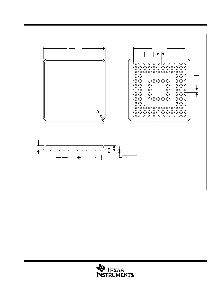
MECHANICAL DATA
MPBG179A � FEBRUARY 2001 � REVISED JANUARY 2002
1
POST OFFICE BOX 655303
�
DALLAS, TEXAS 75265
GZG (S-PBGA-N289)
PLASTIC BALL GRID ARRAY
0,08
M
0,05
0,50
0,50
1,20 MAX
0,85
0,25
0,35
0,30
0,20
0,95
12,10
11,90
SQ
4173512-6/D 11/01
Seating Plane
8
L
B
A
1
F
D
C
E
H
K
G
J
3
2
4
7
5
6
R
M
P
N
V
T
U
W
AA
Y
15
11
9
10
13
12 14
18
17
16
21
19
20
10,00 TYP
A1 Corner
Bottom View
NOTES: A. All linear dimensions are in millimeters.
B. This drawing is subject to change without notice.
C. MicroStar BGA
configuration
MicroStar BGA is a trademark of Texas Instruments.