
www.ti.com
FEATURES
DESCRIPTION
APPLICATIONS
ONET4201PA
SLLS652 ≠ NOVEMBER 2005
155 Mbps to 4.25 Gbps Limiting Amplifier With LOS and RSSI
∑
Multi-Rate Operation from 155 Mbps up to
The ONET4201PA is a versatile high-speed, 3.3-V
4.25 Gbps
limiting amplifier for multiple fiber optic applications
with data rates up to 4.25 Gbps.
∑
89 mW Power Consumption
∑
Input Offset Cancellation
This device provides a gain of about 50 dB, which
ensures a fully differential output swing for input
∑
High Input Dynamic Range
signals as low as 3 mV
p-p
.
∑
Output Disable
The high input signal dynamic range ensures low
∑
CML Data Outputs
jitter output signals even when overdriven with input
∑
Receive Signal Strength Indicator (RSSI)
signal swings as high as 1200 mV
p-p
.
∑
Loss of Signal Detection
The ONET4201PA provides a loss of signal detection
∑
Polarity Select
as well as a received signal strength indicator.
∑
Single 3.3-V Supply
The part is available in a small footprint 3-mm
◊
∑
Surface Mount Small Footprint 3-mm
◊
3-mm
3-mm 16-pin QFN package and is pin-compatible with
16-Pin QFN Package
the ONET2501PA and ONET3301PA.
∑
Pin-Compatible with the ONET2501PA and
This
power
efficient
limiting
amplifier
typically
ONET3301PA
dissipates less than 89 mW and it is characterized for
operation from ≠40
∞
C to 85
∞
C.
∑
Multi-Rate OC3 to OC-48 FEC SONET/SDH
Transmission Systems
∑
1.0625 Gbps, 2.125 Gbps, and 4.25 Gbps Fibre
Channel Receivers
∑
Gigabit Ethernet Receivers
Please be aware that an important notice concerning availability, standard warranty, and use in critical applications of Texas
Instruments semiconductor products and disclaimers thereto appears at the end of this data sheet.
PRODUCTION DATA information is current as of publication date.
Copyright © 2005, Texas Instruments Incorporated
Products conform to specifications per the terms of the Texas
Instruments standard warranty. Production processing does not
necessarily include testing of all parameters.
www.ti.com
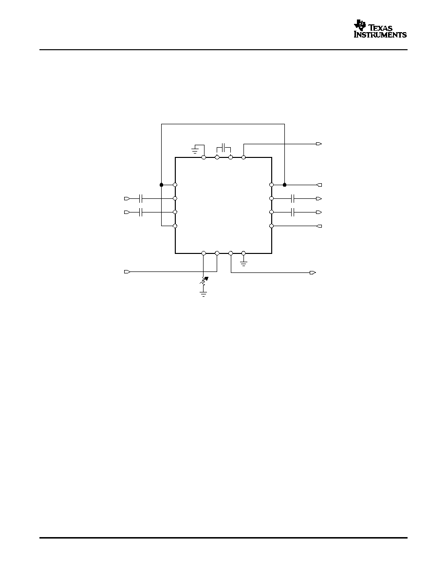
BLOCK DIAGRAM
Input Buffer
DOUT+
DOUT-
DIN+
DIN-
+
Gain Stage
+
+
+
COC2
COC1
DISABLE
LOS
TH
VCC
GND
OUTPOL
Bandgap Voltage
Reference and
Bias Current
Generation
Gain Stage
Gain Stage
Loss of Signal
and
RSSI Detection
Offset
Cancellation
-
RSSI
CML
Output
Buffer
+
-
-
-
-
B0052-01
HIGH SPEED DATA PATH
LOSS OF SIGNAL AND RSSI DETECTION
ONET4201PA
SLLS652 ≠ NOVEMBER 2005
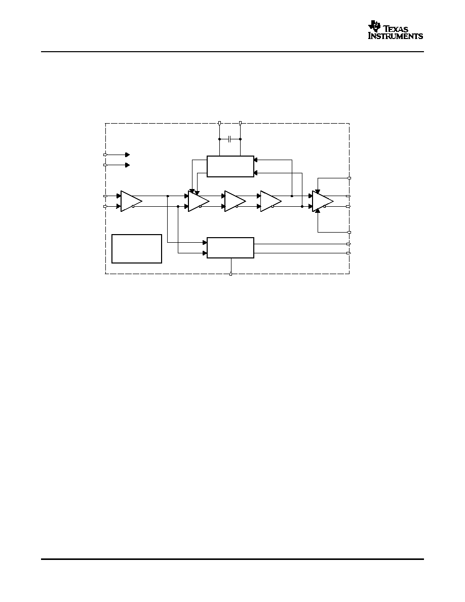
A simplified block diagram of the ONET4201PA is shown in
Figure 1
.
This compact, low power 4.25 Gbps limiting amplifier consists of a high-speed data path with offset cancellation
block, a loss of signal and RSSI detection block, and a bandgap voltage reference and bias current generation
block.
Figure 1. Simplified Block Diagram of the ONET4201PA
The high-speed data signal is applied to the data path by means of the input signal pins DIN+/DIN≠. The data
path consists of the input stage with 2
◊
50-
on-chip line termination to VCC, three gain stages, which provide
the required typical gain of about 50 dB, and a CML output stage. The amplified data output signal is available at
the output pins DOUT+/DOUT≠, which provide 2
◊
50-
back-termination to VCC. The output stage also includes
a data polarity switching function, which is controlled by the OUTPOL input, and a disable function, controlled by
the signal applied to the DISABLE input pin.
Offset cancellation compensates for internal offset voltages and thus ensures proper operation even for very
small input data signals.
The low frequency cutoff is typically as low as 25 kHz with the built-in filter capacitor.
For applications which require even lower cutoff frequencies, an additional external filter capacitor may be
connected to the COC1/COC2 pins.
The output signal of the input buffer is monitored by the loss of signal and RSSI detection circuitry. In this block a
signal is generated that is linearly proportional to the input amplitude over a wide input voltage range. This signal
is available at the RSSI output pin.
Furthermore, this circuit block compares the input signal to a threshold which can be programmed by means of
an external resistor connected to the TH pin. If the input signal falls below the specified threshold, a loss of signal
is indicated at the LOS pin.
The relation between the LOS assert voltage V
AST
(in mV
p-p
) and the external resistor R
TH
(in k
) connected to
the TH pin can be approximated as given below:
2

www.ti.com
R
TH
[
20.8 k
W
V
AST
mVp
*
p
*
1
)
300
W
(1)
V
AST
[
20.8 mVp
*
p
R
TH
k
W *
0.3
)
1 mVp
*
p
(2)
BANDGAP VOLTAGE AND BIAS GENERATION
PACKAGE
GND
COC2
COC1
RSSI
1
2
3
4
VCC
DIN+
DIN-
VCC
RGT PACKAGE
(TOP VIEW)
12
11
10
9
16
VCC
DOUT+
DOUT-
OUTPOL
15
14
13
5
6
7
8
TH
DISABLE
LOS
GND
P0019-01
EP
ONET4201PA
SLLS652 ≠ NOVEMBER 2005
The ONET4201PA limiting amplifier is supplied by a single 3.3-V
±
10% supply voltage connected to the VCC
pins. This voltage is referred to ground (GND).
An on-chip bandgap voltage circuit generates a supply voltage independent reference from which all other
internally required voltages and bias currents are derived.
For the ONET4201PA a small footprint 3-mm
◊
3-mm 16-pin QFN package, with a lead pitch of 0,5 mm, is used.
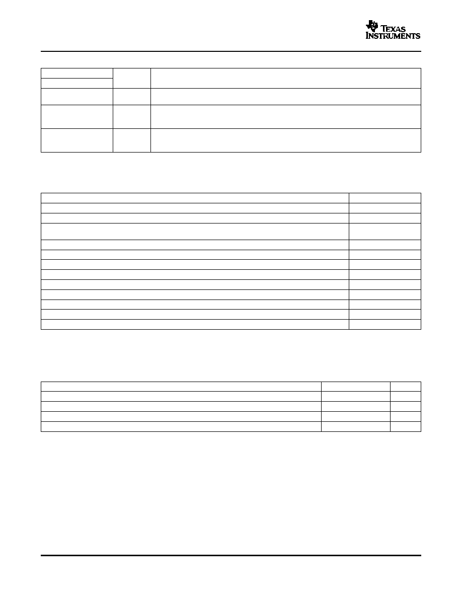
The pin out is shown in
Figure 2
.
Figure 2. Pinout of ONET4201PA in a 3mm x 3mm 16 Pin QFN Package (Top View)
TERMINAL FUNCTIONS
TERMINAL
TYPE
DESCRIPTION
NO.
NAME
1, 4, 12
VCC
supply
3.3-V
±
10% supply voltage
2
DIN+
analog-in
Non-inverted data input. On-chip 50-
terminated to VCC.
3
DIN≠
analog-in
Inverted data input. On-chip 50-
terminated to VCC.
5
TH
analog-in
LOS threshold adjustment with resistor to GND.
6
DISABLE
CMOS-in
Disables CML output stage when set to high level.
7
LOS
CMOS-out
High level indicates that the input signal amplitude is below the programmed threshold level.
8, 16, EP
GND
supply
Circuit ground. Exposed die pad (EP) must be grounded.
Output data signal polarity select (internally pulled high). Setting to a high level or leaving the pin
9
OUTPOL
CMOS-in
open selects normal polarity. Low level selects inverted polarity.
10
DOUT≠
CML-out
Inverted data output. On-chip 50-
back-terminated toVCC.
11
DOUT+
CML-out
Non-inverted data output. On-chip 50-
back-terminated to VCC.
3
www.ti.com
ABSOLUTE MAXIMUM RATINGS
RECOMMENDED OPERATING CONDITIONS
ONET4201PA
SLLS652 ≠ NOVEMBER 2005
TERMINAL FUNCTIONS (continued)
TERMINAL
TYPE
DESCRIPTION
NO.
NAME
Analog output voltage proportional to the input data amplitude. Indicates the strength of the
13
RSSI
analog-out
received signal (RSSI).
Offset cancellation filter capacitor terminal 1. Connect an additional filter capacitor between this pin
14
COC1
analog
and COC2 (pin 15).
To disable the offset cancellation loop connect COC1 and COC2 (pins 14 and 15).
Offset cancellation filter capacitor terminal 2. Connect an additional filter capacitor between this pin
15
COC2
analog
and COC1 (pin 14).
To disable the offset cancellation loop connect COC1 and COC2 (pins 14 and 15).
over operating free-air temperature range (unless otherwise noted)
(1)
VALUE/UNIT
V
CC
Supply voltage
(2)
≠0.3 V to 4.0 V
V
DIN+
, V
DIN-
Voltage at DIN+, DIN≠
(2)
0.5 V to 4.0 V
V
TH
, V
DISABLE
, V
LOS
, V
OUTPOL
, V
DOUT+
,
Voltage at TH, DISABLE, LOS, OUTPOL, DOUT+, DOUT-, RSSI,
≠0.3 V to 4.0 V
V
DOUT≠
, V
RSSI
, V
COC1
, V
COC2
COC1, COC2
(2)
V
COC,DIFF
Differential voltage between COC1 and COC2
±1 V
V
DIN,DIFF
Differential voltage between DIN+ and DIN≠
±2.5 V
I
LOS
Current into LOS
-1 to 9 mA
I
DIN+
, I
DIN≠
, I
DOUT+
, I
DOUT≠
Continuous current at inputs and outputs
≠25 mA to 25 mA
ESD
ESD rating at all pins
2 kV (HBM)
T
J(max)
Maximum junction temperature
125∞C
T
STG
Storage temperature range
≠65 to 85∞C
T
A
Characterized free-air operating temperature range
≠40 to 85∞C
T
LEAD
Lead temperature 1,6 mm (1/16 inch) from case for 10 seconds
260∞C
(1)
Stresses beyond those listed under "absolute maximum ratings" may cause permanent damage to the device. These are stress ratings
only, and functional operation of the device at these or any other conditions beyond those indicated under "recommended operating
conditions" is not implied. Exposure to absolute-maximum-rated conditions for extended periods may affect device reliability.
(2)
All voltage values are with respect to network ground terminal.
MIN
TYP
MAX
UNIT
V
CC
Supply voltage
3
3.3
3.6
V
T
A
Operating free-air temperature
≠40
85
∞
C
V
IH
CMOS input high voltage
2.1
V
V
IL
CMOS input low voltage
0.6
V
4
www.ti.com
DC ELECTRICAL CHARACTERISTICS
AC ELECTRICAL CHARACTERISTICS
ONET4201PA
SLLS652 ≠ NOVEMBER 2005
over recommended operating conditions (unless otherwise noted)
PARAMETER
TEST CONDITIONS
MIN
TYP
MAX
UNIT
V
CC
Supply voltage
3
3.3
3.6
V
DISABLE = low (includes CML output current)
35
45
I
VCC
Supply current
mA
DISABLE = low (excludes CML output current)
27
35
DISABLE = high
0.25
10
V
OD
Differential data output voltage swing
mV
p-p
DISABLE = low, 5 mV
p-p
V
IN
1200 mV
p-p
520
760
1200
R
IN
, R
OUT
Data input/output resistance
Single-ended
50
Input = 8 mV
p-p
, R
RSSI
10 k
200
RSSI output voltage
mV
Input = 80 mV
p-p
, R
RSSI
10 k
1900
RSSI linearity
8 mV
p-p
V
IN
80 mV
p-p
±
3%
V
IN(MIN)
Data input sensitivity
BER < 10
≠10
3
5
mV
p-p
V
IN(MAX)
Data input overload
1200
mV
p-p
LOS high voltage
I
SOURCE
= 30 µA
2.4
V
LOS low voltage
I
SINK
= 1 mA
0.4
V
over recommended operating conditions, typical operating condition is at V
CC
= 3.3 V and T
A
= 25
∞
C (unless otherwise noted)
PARAMETER
TEST CONDITIONS
MIN
TYP
MAX
UNIT
C
OC
= open
25
Low frequency ≠3 dB bandwidth
kHz
C
OC
= 0.54 µF
0.8
Data rate
4.25
Gb/s
v
NI
Input referred noise
230
µV
RMS
K28.5 pattern at 4.25 Gbps
3
19
DJ
Deterministic jitter
K28.5 pattern at 2.125 Gbps
4
35
ps
p-p
K28.5 pattern at 1.0625 Gbps
4
72
Input = 5 mVpp
9
RJ
Random jitter
ps
RMS
Input = 10 mVpp
4
t
R
Output rise time
20% to 80%
45
85
ps
t
F
Output fall time
20% to 80%
45
85
ps
LOS hysteresis
K28.5 pattern at 4.25 Gbps, 20log (V
DEA
/V
AST
)
2.5
4.5
dB
R
TH
LOS threshold adjustment resistor
See
(1)
1.2
6.8
k
range
R
TH
= 2.5 k
, K28.5 pattern at 4.25 Gbps
(1)
10
V
AST
LOS assert voltage
mV
p-p
R
TH
= 6.8 k
, K28.5 pattern at 4.25 Gbps
(1)
2
5
R
TH
= 2.5 k
, K28.5 pattern at 4.25 Gbps
(1)
17
V
DEA
LOS de-assert voltage
mV
p-p
R
TH
= 6.8 k
, K28.5 pattern at 4.25 Gbps
(1)
8
20
T
LOS
LOS assert/deassert time
2
100
µs
T
DIS
Disable response time
20
ns
(1)
For a given external resistor connected to the TH pin the LOS assert voltage value may vary due to part-to-part variations. If high
precision is required, adjustment of this resistor for each device is mandatory.
5
www.ti.com
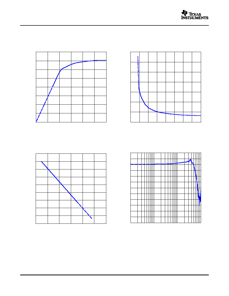
TYPICAL CHARACTERISTICS
V
ID
- Differential Input Voltage - mV
P-P
0
100
200
300
400
500
600
700
800
0
1
2
3
4
5
6
V
O
D
- Differential Output V
oltage - mV
P
-
P
G001
V
ID
- Differential Input Voltage - mV
P-P
0
2
4
6
8
10
12
14
0
5
10
15
20
25
30
35
40
Random Jitter - ps
R
M
S
G002
0
5
10
15
20
25
30
35
40
45
50
55
60
f - Frequency - GHz
Small Signal Gain - dB
0.01
10
0.1
1
G004
V
ID
- Differential Input Voltage - mV
P-P
1
2
3
4
5
6
7
Bit Error Ratio
10
-18
10
0
10
-2
10
-4
10
-6
10
-8
10
-10
10
-12
10
-14
10
-16
G003
ONET4201PA
SLLS652 ≠ NOVEMBER 2005
Typical operating condition is at V
CC
= 3.3 V and T
A
= 25
∞
C (unless otherwise noted).
TRANSFER FUNCTION
RANDOM JITTER
vs INPUT AMPLITUDE
Figure 3.
Figure 4.
BIT-ERROR RATIO
FREQUENCY RESPONSE
INPUT AMPLITUDE
Figure 5.
Figure 6.
6

www.ti.com
t - Time - 50 ps/Div
V
O
D
- Differential Output V
oltage - 160 mV/Div
G005
t - Time - 50 ps/Div
V
O
D
- Differential Output V
oltage - 160 mV/Div
G006
t - Time - 50 ps/Div
V
O
D
- Differential Output V
oltage - 160 mV/Div
G007
ONET4201PA
SLLS652 ≠ NOVEMBER 2005
TYPICAL CHARACTERISTICS (continued)
Typical operating condition is at V
CC
= 3.3 V and T
A
= 25
∞
C (unless otherwise noted).
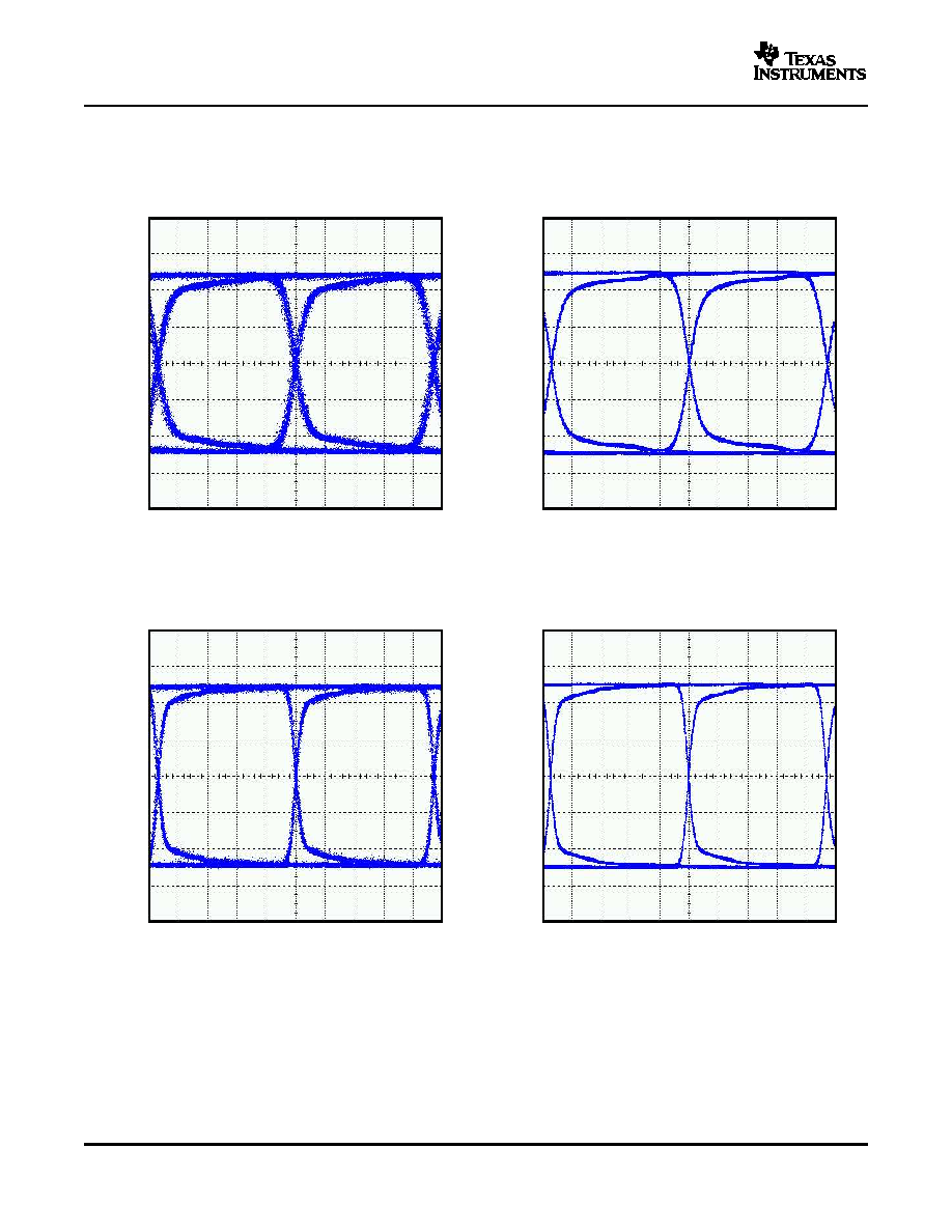
OUTPUT EYE-DIAGRAM AT 4.25 GBPS
OUTPUT EYE-DIAGRAM AT 4.25 GBPS
AND MINIMUM INPUT VOLTAGE (5 mV
p-p
)
AND MAXIMUM INPUT VOLTAGE (1200 mV
p-p
)
Figure 7.
Figure 8.
OUTPUT EYE-DIAGRAM AT 4.25 GBPS AND 85
∞
C
AND MINIMUM INPUT VOLTAGE (5 mV
p-p
)
Figure 9.
7
www.ti.com
t - Time - 100 ps/Div
V
O
D
- Differential Output V
oltage - 160 mV/Div
G008
t - Time - 100 ps/Div
V
O
D
- Differential Output V
oltage - 160 mV/Div
G009
t - Time - 200 ps/Div
V
O
D
- Differential Output V
oltage - 160 mV/Div
G010
t - Time - 200 ps/Div
V
O
D
- Differential Output V
oltage - 160 mV/Div
G011
ONET4201PA
SLLS652 ≠ NOVEMBER 2005
TYPICAL CHARACTERISTICS (continued)
Typical operating condition is at V
CC
= 3.3 V and T
A
= 25
∞
C (unless otherwise noted).
OUTPUT EYE-DIAGRAM AT 2.125 GBPS
OUTPUT EYE-DIAGRAM AT 2.125 GBPS
AND MINIMUM INPUT VOLTAGE (5 mV
p-p
)
AND MAXIMUM INPUT VOLTAGE (1200 mV
p-p
)
Figure 10.
Figure 11.
OUTPUT EYE-DIAGRAM AT 1.0625 GBPS
OUTPUT EYE-DIAGRAM AT 1.0625 GBPS
AND MINIMUM INPUT VOLTAGE (5 mV
p-p
)
AND MAXIMUM INPUT VOLTAGE (1200 mV
p-p
)
Figure 12.
Figure 13.
8
www.ti.com
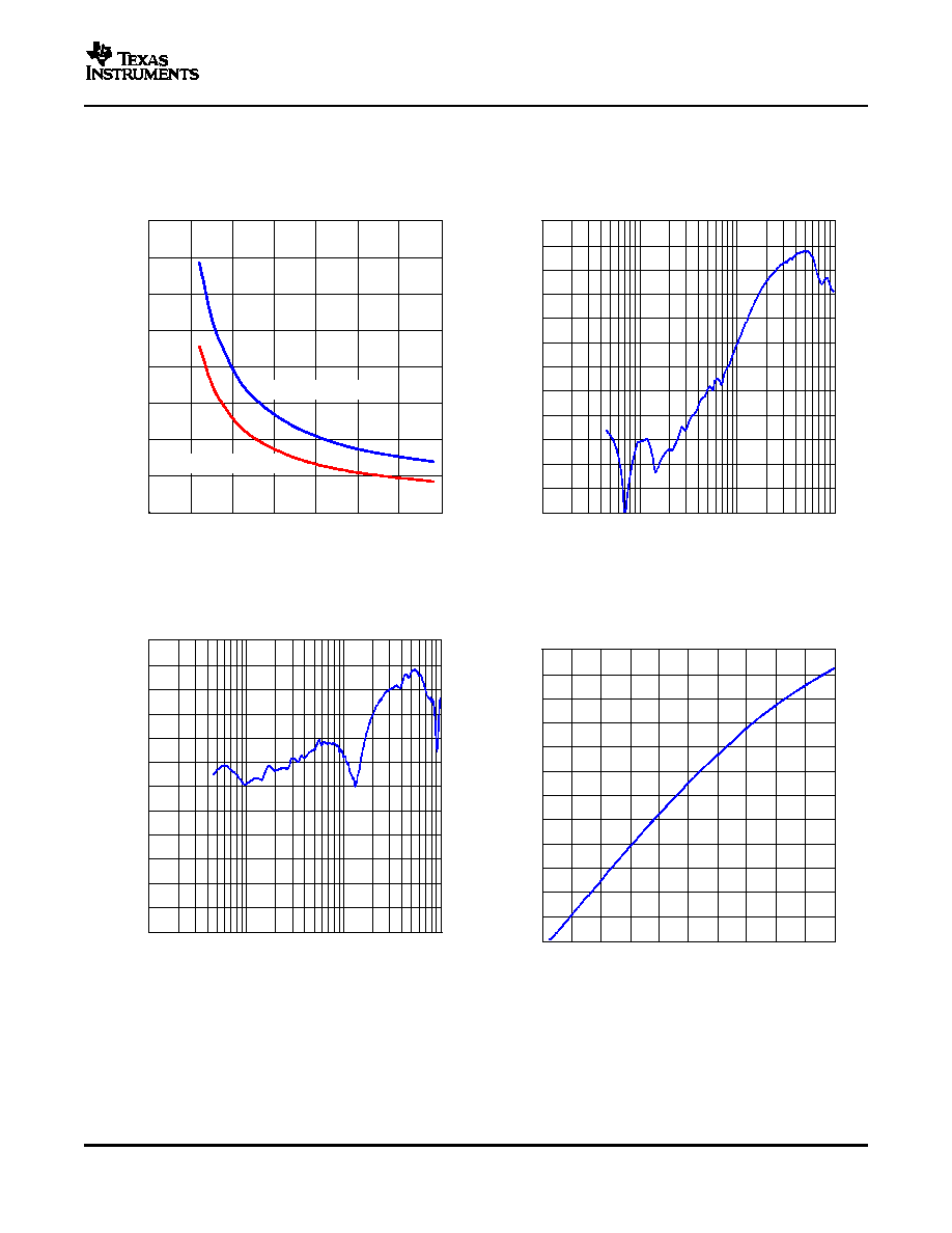
R
th
- Threshold Resistance - k
0
5
10
15
20
25
30
35
40
0
1
2
3
4
5
6
7
LOS Assert/Deassert V
oltage - mV
P
-
P
LOS Deassert Voltage
LOS Assert Voltage
G012
-60
-55
-50
-45
-40
-35
-30
-25
-20
-15
-10
-5
0
SDD1
1 - Differential Input Return Gain - dB
f - Frequency - MHz
G013
10
10k
100
1k
-60
-55
-50
-45
-40
-35
-30
-25
-20
-15
-10
-5
0
SDD22 - Differential Output Return Gain - dB
f - Frequency - MHz
G014
10
10k
100
1k
V
ID
- Differential Input Voltage - mV
P-P
0
200
400
600
800
1000
1200
1400
1600
1800
2000
2200
2400
0
10
20
30
40
50
60
70
80
90
100
RSSI - Receive Signals Strength Indicator V
oltage - mV
G015
ONET4201PA
SLLS652 ≠ NOVEMBER 2005
TYPICAL CHARACTERISTICS (continued)
Typical operating condition is at V
CC
= 3.3 V and T
A
= 25
∞
C (unless otherwise noted).
ASSERT/DEASSERT VOLTAGE
DIFFERENTIAL INPUT RETURN GAIN
vs THRESHOLD RESISTANCE
vs FREQUENCY
Figure 14.
Figure 15.
DIFFERENTIAL OUTPUT RETURN GAIN
RSSI VOLTAGE
vs FREQUENCY
vs INPUT AMPLITUDE
Figure 16.
Figure 17.
9
www.ti.com
APPLICATION INFORMATION
VCC
DIN+
DIN-
DISABLE
LOS
DOUT-
DOUT+
GND
DIN+
DIN-
DOUT-
DOUT+
GND
VCC
OUTPOL
VCC
VCC
RSSI
LOS
DISABLE
ONET4201PA
16-Pin QFN
COC2
COC1
OUTPOL
TH
RSSI
C
OC
Optional
C
1
C
2
C
3
C
4
R
TH
S0072-01
ONET4201PA
SLLS652 ≠ NOVEMBER 2005
Figure 18
shows the ONET4201PA connected with an ac-coupled interface to the data signal source as well as
to the output load.
Besides the ac-coupling capacitors C
1
through C
4
in the input and output data signal lines, the only required
external component is the LOS threshold setting resistor R
th
. In addition, an optional external filter capacitor
(C
OC
) may be used if a lower cutoff frequency is desired.
Figure 18. Basic Application Circuit With AC-Coupled I/Os
10
PACKAGING INFORMATION
Orderable Device
Status
(1)
Package
Type
Package
Drawing
Pins Package
Qty
Eco Plan
(2)
Lead/Ball Finish
MSL Peak Temp
(3)
ONET4201PARGTR
ACTIVE
QFN
RGT
16
3000 Green (RoHS &
no Sb/Br)
CU
Level-2-260C-1 YEAR
ONET4201PARGTRG4
ACTIVE
QFN
RGT
16
3000 Green (RoHS &
no Sb/Br)
CU
Level-2-260C-1 YEAR
ONET4201PARGTT
ACTIVE
QFN
RGT
16
250
Green (RoHS &
no Sb/Br)
CU
Level-2-260C-1 YEAR
ONET4201PARGTTG4
ACTIVE
QFN
RGT
16
250
Green (RoHS &
no Sb/Br)
CU
Level-2-260C-1 YEAR
(1)
The marketing status values are defined as follows:
ACTIVE: Product device recommended for new designs.
LIFEBUY: TI has announced that the device will be discontinued, and a lifetime-buy period is in effect.
NRND: Not recommended for new designs. Device is in production to support existing customers, but TI does not recommend using this part in
a new design.
PREVIEW: Device has been announced but is not in production. Samples may or may not be available.
OBSOLETE: TI has discontinued the production of the device.
(2)
Eco Plan - The planned eco-friendly classification: Pb-Free (RoHS), Pb-Free (RoHS Exempt), or Green (RoHS & no Sb/Br) - please check
http://www.ti.com/productcontent
for the latest availability information and additional product content details.
TBD: The Pb-Free/Green conversion plan has not been defined.
Pb-Free (RoHS): TI's terms "Lead-Free" or "Pb-Free" mean semiconductor products that are compatible with the current RoHS requirements
for all 6 substances, including the requirement that lead not exceed 0.1% by weight in homogeneous materials. Where designed to be soldered
at high temperatures, TI Pb-Free products are suitable for use in specified lead-free processes.
Pb-Free (RoHS Exempt): This component has a RoHS exemption for either 1) lead-based flip-chip solder bumps used between the die and
package, or 2) lead-based die adhesive used between the die and leadframe. The component is otherwise considered Pb-Free (RoHS
compatible) as defined above.
Green (RoHS & no Sb/Br): TI defines "Green" to mean Pb-Free (RoHS compatible), and free of Bromine (Br) and Antimony (Sb) based flame
retardants (Br or Sb do not exceed 0.1% by weight in homogeneous material)
(3)
MSL, Peak Temp. -- The Moisture Sensitivity Level rating according to the JEDEC industry standard classifications, and peak solder
temperature.
Important Information and Disclaimer:The information provided on this page represents TI's knowledge and belief as of the date that it is
provided. TI bases its knowledge and belief on information provided by third parties, and makes no representation or warranty as to the
accuracy of such information. Efforts are underway to better integrate information from third parties. TI has taken and continues to take
reasonable steps to provide representative and accurate information but may not have conducted destructive testing or chemical analysis on
incoming materials and chemicals. TI and TI suppliers consider certain information to be proprietary, and thus CAS numbers and other limited
information may not be available for release.
In no event shall TI's liability arising out of such information exceed the total purchase price of the TI part(s) at issue in this document sold by TI
to Customer on an annual basis.
PACKAGE OPTION ADDENDUM
www.ti.com
12-Jan-2006
Addendum-Page 1


IMPORTANT NOTICE
Texas Instruments Incorporated and its subsidiaries (TI) reserve the right to make corrections, modifications,
enhancements, improvements, and other changes to its products and services at any time and to discontinue
any product or service without notice. Customers should obtain the latest relevant information before placing
orders and should verify that such information is current and complete. All products are sold subject to TI's terms
and conditions of sale supplied at the time of order acknowledgment.
TI warrants performance of its hardware products to the specifications applicable at the time of sale in
accordance with TI's standard warranty. Testing and other quality control techniques are used to the extent TI
deems necessary to support this warranty. Except where mandated by government requirements, testing of all
parameters of each product is not necessarily performed.
TI assumes no liability for applications assistance or customer product design. Customers are responsible for
their products and applications using TI components. To minimize the risks associated with customer products
and applications, customers should provide adequate design and operating safeguards.
TI does not warrant or represent that any license, either express or implied, is granted under any TI patent right,
copyright, mask work right, or other TI intellectual property right relating to any combination, machine, or process
in which TI products or services are used. Information published by TI regarding third-party products or services
does not constitute a license from TI to use such products or services or a warranty or endorsement thereof.
Use of such information may require a license from a third party under the patents or other intellectual property
of the third party, or a license from TI under the patents or other intellectual property of TI.
Reproduction of information in TI data books or data sheets is permissible only if reproduction is without
alteration and is accompanied by all associated warranties, conditions, limitations, and notices. Reproduction
of this information with alteration is an unfair and deceptive business practice. TI is not responsible or liable for
such altered documentation.
Resale of TI products or services with statements different from or beyond the parameters stated by TI for that
product or service voids all express and any implied warranties for the associated TI product or service and
is an unfair and deceptive business practice. TI is not responsible or liable for any such statements.
Following are URLs where you can obtain information on other Texas Instruments products and application
solutions:
Products
Applications
Amplifiers
amplifier.ti.com
Audio
www.ti.com/audio
Data Converters
dataconverter.ti.com
Automotive
www.ti.com/automotive
DSP
dsp.ti.com
Broadband
www.ti.com/broadband
Interface
interface.ti.com
Digital Control
www.ti.com/digitalcontrol
Logic
logic.ti.com
Military
www.ti.com/military
Power Mgmt
power.ti.com
Optical Networking
www.ti.com/opticalnetwork
Microcontrollers
microcontroller.ti.com
Security
www.ti.com/security
Telephony
www.ti.com/telephony
Video & Imaging
www.ti.com/video
Wireless
www.ti.com/wireless
Mailing Address:
Texas Instruments
Post Office Box 655303 Dallas, Texas 75265
Copyright 2006, Texas Instruments Incorporated