
www.ti.com
FEATURES
APPLICATIONS
DESCRIPTION
ONET4211LD
SLLS688 ≠ NOVEMBER 2005
155 Mbps to 4.25 Gbps LASER DRIVER
∑
SONET/SDH Transmission Systems
∑
Multirate Operation From 155 Mbps up to
4.25 Gbps
∑
Fibre Channel Optical Modules
∑
Fiber Optic Data Links
∑
Bias Current Programmable From 1 mA
to 100 mA
∑
Digital Cross-Connects
∑
Optical Transmitters
∑
Modulation Current Programmable From 5 mA
to 85 mA
∑
APC and Fault Detection
∑
Fault Mode Selection
The ONET4211LD is a laser driver for multiple fiber
optic applications up to 4.25 Gbps. The device
∑
Bias and Photodiode Current Monitors
accepts CML input data and provides bias and
∑
CML Data Inputs
modulation currents for driving a laser diode. Also
∑
Temperature Compensation of Modulation
provided
are
automatic
power
control
(APC),
temperature compensation of modulation current,
Current
fault detection, and current monitor features.
∑
Single 3.3-V Supply
The device is available in a small-footprint, 4 mm
◊
4
∑
Surface-Mount, Small-Footprint, 4 mm
◊
4 mm
mm 24-pin QFN package. The circuit requires a
24-Lead QFN Package
single 3.3-V supply.
A
This power-efficient laser driver is characterized for
operation from ≠40
∞
C to 85
∞
C.
Please be aware that an important notice concerning availability, standard warranty, and use in critical applications of Texas
Instruments semiconductor products and disclaimers thereto appears at the end of this data sheet.
PRODUCTION DATA information is current as of publication date.
Copyright © 2005, Texas Instruments Incorporated
Products conform to specifications per the terms of the Texas
Instruments standard warranty. Production processing does not
necessarily include testing of all parameters.
www.ti.com
DETAILED DESCRIPTION
BLOCK DIAGRAM
B0092-01
VCC
GND
DIN+
DIN-
MOD+
MOD-
MODSET
Current Modulator
OUTPOL
MODTC
BIAS
MONB
IBMAX
MONP
PD
APCSET
SDOWN
DISABLE
CAPC
FLTMODE
Input Buffer Stage
Modulation Current Generator
MODCTRL
MODSET
IMODEN
MODTC
IMODMON
Reference
Voltage
and Bias
Generation
VCC
GND
4
3
Bias Current Generator
BIAS
IBMAX
IBEN
IBMON
IBSET
MONB
Control
IMODEN
IMODMON
IBEN
IBMON
DISABLE
SDOWN
APCCTRL
APCMON
FLTMODE
Automatic Power Control
(APC)
IBSET
APCMON
APCCTRL
MONP
APCSET
PD
CAPC
ONET4211LD
SLLS688 ≠ NOVEMBER 2005
These devices have limited built-in ESD protection. The leads should be shorted together or the device
placed in conductive foam during storage or handling to prevent electrostatic damage to the MOS gates.
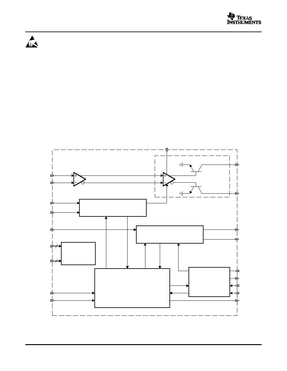
A simplified block diagram of the ONET4211LD is shown in
Figure 1
.
This compact, low-power, 4.25-Gbps laser driver circuit consists of a high-speed data path and a
bias-and-control block.
The function of the data path is to buffer the input data and then modulate the laser diode current according to
the input data stream.
The bias-and-control block generates the laser diode bias current, contains automatic power control (APC) to
maintain constant optical output power, generates a modulation current that can be temperature compensated,
and controls power on during start-up and shutdown after failure detection. The circuit design is optimized for
high-speed and low-voltage operation (3.3 V).
The main circuit blocks are described in detail in the following paragraphs.
Figure 1. Simplified Block Diagram of the ONET4211LD
2

www.ti.com
HIGH-SPEED DATA PATH
BIAS AND CONTROL
BANDGAP VOLTAGE AND BIAS GENERATION
AUTOMATIC POWER CONTROL
I
PD
[A]
+
P
AVG
[W]
Ú
MON
[A W]
(1)
R
APCSET
[
W
]
+
4.69 V
I
PD
[A]
+
4.69 V
P
AVG
[W]
Ú
MON
[A W]
(2)
I
BIASMAX
[A]
+
343 V
R
BIASMAX
[
W
]
(3)
V
MONB
[V]
+
R
MONB
[
W
]
I
BIAS
[A]
68
(4)
ONET4211LD
SLLS688 ≠ NOVEMBER 2005
DETAILED DESCRIPTION (continued)
The high-speed data path consists of an input buffer stage and a current modulator.
The input buffer stage takes CML-compatible differential signals. It provides on-chip, 50-
termination to VCC.
AC-coupling may be used at the DIN+ and DIN- inputs.
The laser diode current modulator consists mainly of two common-emitter output transistors and the required
driver circuitry. According to the input data stream, the modulation current is sunk at the MOD+ or the MOD≠ pin.
Modulation current setting is performed by means of the modulation current generator block, which is supervised
by the control circuit block.
The laser diode can be either ac- or dc-coupled. In either case, the maximum modulation current is 85 mA. The
modulation output is optimized for driving a 20-
load.
For optimum power efficiency, the laser driver does not provide any on-chip back-termination.
The bias-and-control circuitry consists of the bandgap voltage and bias generation block, the bias current
generator, the automatic power control block, and the supervising control circuitry.
The bandgap voltage reference provides the process- and temperature-independent reference voltages needed
to set bias current, modulation current, and photodiode reference current. Additionally, this block provides the
biasing for all internal circuits.
The ONET4211LD laser driver incorporates an APC loop to compensate for the changes in laser threshold
current over temperature and lifetime. The internal APC is enabled when resistors are connected to the IBMAX
and APCSET pins. A back-facet photodiode mounted in the laser package is used to detect the average laser
output power. The photodiode current I
PD
that is proportional to the average laser power can be calculated by
using the laser-to-monitor transfer ratio,
MON
and the average power, P
AVG
:
In closed-loop operation, the APC modifies the laser diode bias current by comparing I
PD
with a reference current
I
APCSET
and generates a bias compensation current. I
PD
can be programmed by selecting the external resistor
R
APCSET
according to:
The bias compensation current subtracts from the maximum bias current to maintain the monitor photodiode
current. The maximum bias current is programmed by the resistor connected to IBMAX:
An external pin, MONB, is provided as a bias current monitor output. A fraction of the bias current (1/68) is
mirrored and develops a voltage drop across an external resistor to ground, R
MONB
. The voltage at MONB is
given as:
If the voltage at MONB is greater than the programmed threshold, a fault mode occurs.
MONP is also provided as a photocurrent monitor output. The photodiode current, I
PD
, is mirrored and develops a
voltage across an external resistor to ground, R
MONP
. The voltage at MONP is given as:
3

www.ti.com
V
MONP
[V]
+
R
MONP
[
W
]
I
PD
[A]
(5)
MODULATION CURRENT GENERATOR
I
MOD
[A]
+
265 V
R
MODSET
[
W
]
1
)
24
W
R
MODTC
[
W
]
)
630 ppm
T[
o
C]
*
T
0
[
o
C]
(6)
CONTROL
FAULT DETECTION
ONET4211LD
SLLS688 ≠ NOVEMBER 2005
DETAILED DESCRIPTION (continued)
If the voltage at MONP is greater than the programmed threshold, a fault mode occurs.
As with any negative-feedback system design, care must be taken to ensure stability of the loop. The loop
bandwidth must not be too high, in order to minimize pattern-dependent jitter. The dominant pole is determined
by the capacitor C
APC
. The recommended value for C
APC
is 200 nF. The capacitance of the monitor photodiode
C
PD
adds another pole to the system, and thus it must be small enough to maintain stability. The recommended
value for this capacitance is C
PD
50 pF.
The internal APC loop can be disabled by connecting a 100-k
resistor from APCSET to VCC and leaving PD
open. In open-loop operation, the laser diode current is set by I
BIASMAX
and I
MODSET
.
The modulation current generator defines the tail current of the modulator, which is sunk from either MOD+ or
MOD≠, depending on the data pattern. The modulation current consists of a current I
MOD0
at a reference
temperature T
0
= 60
∞
C (set by the resistor R
MODSET
) and a temperature-dependent modulation current defined by
the resistor R
MODTC
. The modulation current can be estimated as follows:
Note that the reference temperature, T
0
, and the temperature compensation set by R
MODTC
vary from part to part.
To reduce the variation, I
MOD
can be calibrated over temperature and set with a microcontroller DAC or digital
potentiometer.
The function of this block is to control the start-up sequence, detect faults, detect tracking failure of the APC loop,
and provide disable control. The laser driver has a controlled start-up sequence which helps prevent transient
glitches from being applied to the laser during power on. At start-up, the laser diode is off, SDOWN is low, and
the APC loop is open. Once V
CC
reaches ~2.8 V, the laser diode bias generator and modulation current
generator circuitry are activated (if DISABLE is low). The slow-start circuitry gradually brings up the current
delivered to the laser diode. From the time when V
CC
reaches ~2.8 V until the modulation current and bias
current reach 95% of their steady state value, is considered the initialization time. If DISABLE is asserted during
power on, the slow-start circuitry does not activate until DISABLE is negated.
The fault detection circuitry monitors the operation of the ONET4211LD. If FLTMODE is set to a low level,
(hard-fault mode) this circuitry disables the bias and modulation circuits and latches the SDOWN output on
detection of a fault. The fault mode is reset by toggling DISABLE (for a minimum time of T
RES
) or by toggling
VCC.
Once DISABLE is toggled, SDOWN is set low and the circuit is re-initialized.
If FLTMODE is set to a high level (soft-fault mode), a fault is indicated at the SDOWN output; however, the bias
and modulation circuits are not disabled. The SDOWN output is reset once the fault-causing condition
disappears. Toggling DISABLE or VCC is not required.
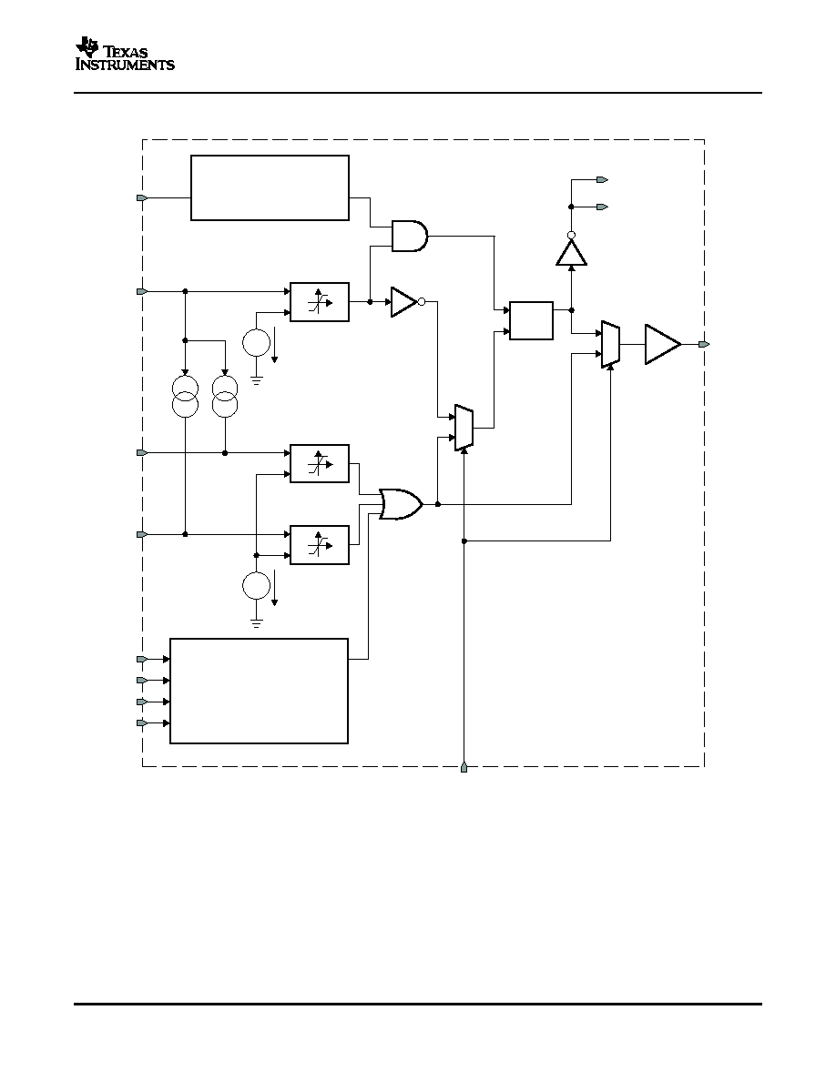
A functional representation of the fault-detection circuitry is shown in
Figure 2
.
4
www.ti.com
B0093-01
DISABLE
SDOWN
Inverter
Inverter
MUX
MUX
IBEN
IMODEN
MONP
MONB
I1
I0
I0
I1
VCC
I
PD
I
BIAS/68
1.25 V
2.8 V
Comparator
Comparator
Flipflop
CMOS
Buffer
Comparator
APCSET
MODSET
MODTC
IBMAX
APCSET
MODSET
MODTC
RES
T
Counter
RES
-
-
S
-
Q
Q
Q
Q
Q
Q
+
+
R
+
SHORT
START
IBMAX
FLTMODE
Short Circuit
to VCC or
GND Detect
+
-
+
-
ONET4211LD
SLLS688 ≠ NOVEMBER 2005
DETAILED DESCRIPTION (continued)
Figure 2. Functional Representation of the Fault Detection Circuitry
A fault mode is produced if the laser cathode is grounded and the photocurrent causes MONP to exceed its
programmed threshold. Another fault mode can be produced if the laser diode end-of-life condition causes
excessive bias current and photocurrent that results in monitor voltages (MONP, MONB) being greater than their
programmed threshold. Other fault modes can occur if there are any I/O pin single-point failures (short to VCC or
GND) and the monitor voltages exceed their programmed threshold (see
Table 1
).
5

www.ti.com
PACKAGE
ONET4211LD
SLLS688 ≠ NOVEMBER 2005
DETAILED DESCRIPTION (continued)
Table 1. Response to I/O-Pin Shorts to VCC or GND
FLTMODE = LOW
FLTMODE = HIGH
PIN
Response to Short to GND
Response to Short to V
CC
Response to Short to GND
Response to Short to V
CC
APCSET
SDOWN latched high, I
BIAS
and
No fault, I
MOD
unaffected
SDOWN high, I
BIAS
and I
MOD
No fault
I
MOD
disabled
unaffected
BIAS
SDOWN latched high, I
MOD
No fault, I
BIAS
goes to zero
SDOWN high, I
MOD
No fault, I
MOD
unaffected
disabled
unaffected
CAPC
No fault
No fault, I
BIAS
goes to zero
No fault, I
MOD
unaffected
No fault, I
BIAS
goes to zero
DIN+
No fault, I
MOD
disabled
No fault
No fault, I
MOD
disabled
No fault
DIN≠
No fault, I
MOD
disabled
No fault
No fault, I
MOD
disabled
No fault
DISABLE
Normal circuit operation
Normal circuit operation
Normal circuit operation
Normal circuit operation
IBMAX
SDOWN latched high, I
BIAS
and
SDOWN latched high, I
BIAS
SDOWN high, I
MOD
SDOWN high, I
MOD
unaffected
I
MOD
disabled
and I
MOD
disabled
unaffected
MOD+
SDOWN latched high, I
BIAS
and
No fault
SDOWN high, I
BIAS
No fault
I
MOD
disabled
unaffected
MOD≠
SDOWN latched high, I
BIAS
and
No fault
SDOWN high, I
BIAS
No fault
I
MOD
disabled
unaffected
MODSET
SDOWN latched high, I
BIAS
and
No fault, I
MOD
disabled
SDOWN high, I
BIAS
No fault, I
MOD
disabled
I
MOD
disabled
unaffected
MODTC
SDOWN latched high, I
BIAS
and
No fault
SDOWN high, I
BIAS
and I
MOD
No fault
I
MOD
disabled
unaffected
MONB
No fault
SDOWN latched high, I
BIAS
No fault
SDOWN high, I
BIAS
and I
MOD
and I
MOD
disabled
unaffected
MONP
No fault
SDOWN latched high, I
BIAS
No fault
SDOWN high, I
BIAS
and I
MOD
and I
MOD
disabled
unaffected
OUTPOL
No fault, polarity reverses
No fault
No fault, polarity reverses
No fault
PD
No fault, I
MOD
unaffected
No fault, I
BIAS
goes to zero
No fault, I
MOD
unaffected
No fault, I
BIAS
goes to zero
SDOWN
No fault
No fault
No fault
No fault
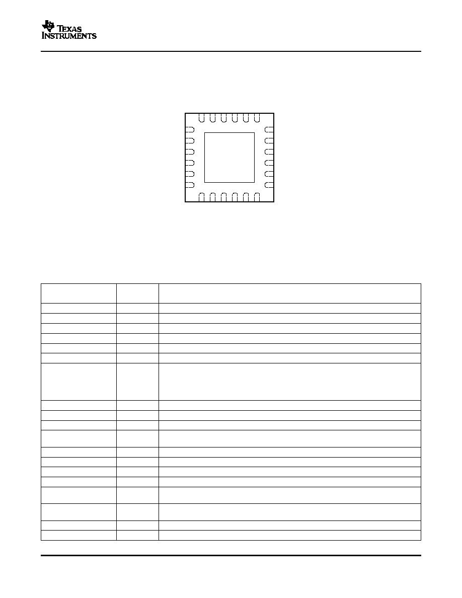
For the ONET4211LD, a small-footprint, 4-mm
◊
4-mm, 24-lead QFN package is used, with a lead pitch of 0,5
mm. The pinout is shown in
Figure 3
.
To achieve the required low thermal resistance of about 38 K/W, which keeps the maximum junction temperature
below 115
∞
C, a good thermal connection of the exposed die pad is mandatory.
6
www.ti.com
P0024-03
GND
DISABLE
VCC
APCSET
MOD-
OUTPOL
MOD+
IBMAX
VCC
CAPC
BIAS
PD
18
17
16
15
14
13
1
2
3
4
5
6
GND
MONP
VCC
MONB
DIN+
SDOWN
DIN-
FL
TMODE
VCC
MODSET
GND
MODTC
24
23
22
21
20
19
7
8
9
10
11
12
RGE PACKAGE
(TOP VIEW)
ONET4211LD
SLLS688 ≠ NOVEMBER 2005
Figure 3. Pinout of the ONET4211LD in a 4-mm
◊
4-mm, 24-Lead QFN Package (Top View)
TERMINAL FUNCTIONS
TERMINAL
TYPE
DESCRIPTION
NAME
NO.
APCSET
23
Analog-in
Set photodiode reference current with resistor to GND.
BIAS
13
Analog-out
Laser-diode bias-current sink. Connect to laser cathode.
CAPC
20
Analog
APC loop capacitor
DIN+
3
CML-in
Non-inverted data input. On-chip, 50-
terminated to VCC.
DIN≠
4
CML-in
Inverted data input. On-chip, 50-
terminated to VCC.
DISABLE
24
LVTTL-in
Disable modulation and bias-current outputs.
FLTMODE
10
CMOS-in
Fault mode selection input. If a low level is applied to this pin, any fault event is latched and the
bias and modulation currents are disabled in a fault condition. Toggling of DISABLE or VCC
resets the fault condition. If pin is set to a high level, fault events are flagged at the SDOWN
output but not latched. The bias and modulation currents are not disabled. SDOWN is reset
once the fault condition disappears.
GND
1, 6, 18, EP
Supply
Circuit ground. The exposed die pad (EP) must be grounded.
IBMAX
21
Analog-in
Set maximum laser diode current with resistor to GND.
MOD+
15
Analog-out
Laser modulation current output. Connect to laser cathode. Avoid usage of vias on board.
MOD≠
16
Analog-out
Complementary laser modulation current output. Connect to VCC adjacent to anode of laser
diode. Avoid usage of vias on board.
MODSET
11
Analog-in
Set temperature-independent modulation current with resistor to GND.
MODTC
12
Analog-in
Set modulation-current temperature compensation with resistor to GND.
MONB
8
Analog-out
Bias current monitor. Sources 1/68 of the bias current.
MONP
7
Analog-out
Photodiode current monitor. Sources a current identical to the photodiode current.
OUTPOL
22
LVTTL-in
Alters modulation current output polarity. Open or high: normal polarity; low: inverted polarity.
OUTPOL is pulled up internally. Normal polarity: when DIN+ is high, current is sunk into MOD+.
PD
19
Analog-in
Monitor photodiode input. Connect to photodiode anode for APC. Sinks the photodiode current
to GND.
SDOWN
9
LVTTL-out
Fault detection flag
VCC
2, 5, 14, 17
Supply
3.3-V,
±
10% supply voltage
7

www.ti.com
ABSOLUTE MAXIMUM RATINGS
ONET4211LD
SLLS688 ≠ NOVEMBER 2005
over operating free-air temperature range (unless otherwise noted)
(1)
V
CC
Supply voltage
(2)
≠0.3 V to 4 V
I
IBIAS
Current into BIAS
≠20 mA to 120 mA
I
IMOD+
, I
IMOD≠
Current into MOD+, MOD≠
≠ 20 mA to 120 mA
I
PD
Current into PD
≠5 mA to 5 mA
V
DIN+
, V
DIN≠,
V
DISABLE
, V
MONB
,
Voltage at DIN+, DIN≠, DISABLE, MONB, MONP, FLTMODE, SDOWN
(2)
≠0.3 V to 4V
V
MONP
, V
FLTMODE
, V
SDOWN
V
CAPC
, V
IBMAX
, V
MODSET
,
Voltage at CAPC, IBMAX, MODSET, APCSET, MODTC
(2)
≠0.3 V to 3 V
V
APCSET
, V
MODTC
V
MOD+
, V
MOD≠
Voltage at MOD+, MOD≠
(2)
0.6 V to VCC + 1.5 V
V
BIAS
Voltage at BIAS
(2)
1 V to 3.5 V
ESD rating at all pins except MOD+, MOD≠
2 kV (HBM)
ESD
ESD rating at MOD+, MOD-
1 kV (HBM)
T
J,max
Maximum junction temperature
150
∞
C
T
STG
Storage temperature range
≠65
∞
C to 150
∞
C
T
A
Characterized free-air operating temperature range
≠40
∞
C to 85
∞
C
T
LEAD
Lead temperature 1,6 mm (1/16 inch) from case for 10 seconds
260
∞
C
(1)
Stresses beyond those listed under absolute maximum ratings may cause permanent damage to the device. These are stress ratings
only, and functional operation of the device at these or any other conditions beyond those indicated under recommended operating
conditions is not implied. Exposure to absolute≠maximum≠rated conditions for extended periods may affect device reliability.
(2)
All voltage values are with respect to network ground terminal.
8
www.ti.com
RECOMMENDED OPERATING CONDITIONS
DC ELECTRICAL CHARACTERISTICS
AC ELECTRICAL CHARACTERISTICS
ONET4211LD
SLLS688 ≠ NOVEMBER 2005
over operating free-air temperature range (unless otherwise noted)
MIN
NOM
MAX
UNIT
V
CC
Supply voltage
3
3.3
3.6
V
T
A
Operating free-air temperature
≠40
85
∞
C
over recommended operating conditions (unless otherwise noted)
PARAMETER
TEST CONDITIONS
MIN
TYP
MAX
UNIT
V
CC
Supply voltage
3
3.3
3.6
V
I
MOD
= 30 mA, I
BIAS
= 20 mA (excluding I
MOD
,
22
mA
I
BIAS
)
I
VCC
Supply current
I
MOD
= 60 mA, I
BIAS
= 100 mA (excluding I
MOD
,
45
mA
I
BIAS
)
I
BIAS
Bias current range
100
mA
DISABLE = high or hard-fault mode; V
BIAS
I
BIAS-OFF
Bias off-current
25
µ
A
3.5 V
During module hot plugging. V
CC
turnon time
Bias overshoot
10%
must be
0.8 s
Bias current temperature stability
APC open loop
≠480
480
ppm/
∞
C
I
BIAS
1 mA
≠15%
15%
Bias current absolute accuracy
(1)
I
BIAS
= 1 mA, T
A
= 25
∞
C
±
15%
Bias current monitor gain, I
BIAS
/I
MONB
68
mA/ mA
A fault is never detected for V
MONB/P
1 V and
MONB and MONP threshold range
1
1.25
1.35
V
a fault always occurs for V
MONB/P
1.35 V
PD current monitor gain, I
PD
/I
MONP
1
mA/mA
VID
Differential input signal
200
1600
mVp-p
SDOWN output high voltage
I
OH
= 100
µ
A sourcing
2.4
V
SDOWN output low voltage
I
OL
= 1 mA sinking
0.4
V
DISABLE input impedance
4.7
7.4
10
k
DISABLE input high voltage
2
V
DISABLE input low voltage
0.8
V
V
PD
Monitor diode voltage
1.6
V
Monitor diode dc current range
18
1500
µ
A
(1)
Absolute accuracy refers to part-to-part variation.
Typical operating condition is at V
CC
= 3.3 V, I
MOD
= 30 mA, I
BIAS
= 20 mA and T
A
= 25
∞
C.
over recommended operating conditions (unless otherwise noted)
PARAMETER
TEST CONDITIONS
MIN
TYP
MAX
UNIT
Data rate
4.25
Gbps
Current into MOD+/MOD≠ pin;
I
MOD
Modulation current range
5
85
mA
V
MOD+
, V
MOD≠
0.6 V
I
MOD-OFF
Modulation off-current
DISABLE = high or hard-fault occurred
25
µ
A
Modulation current stability
≠600
600
ppm/
∞
C
I
MOD
= 10 mA
±
40%
Modulation current absolute
accuracy
(1)
I
MOD
= 80 mA
±
25%
(1)
Absolute accuracy refers to part-to-part variation.
9
www.ti.com
ONET4211LD
SLLS688 ≠ NOVEMBER 2005
AC ELECTRICAL CHARACTERISTICS (continued)
Typical operating condition is at V
CC
= 3.3 V, I
MOD
= 30 mA, I
BIAS
= 20 mA and T
A
= 25
∞
C.
over recommended operating conditions (unless otherwise noted)
PARAMETER
TEST CONDITIONS
MIN
TYP
MAX
UNIT
R
MODTC
= 3.125 k
8300
Modulation current
ppm/
∞
C
temperature compensation
(2)
R
MODTC
open
630
t
r
Output rise time (20% to 80%)
V
MOD+
1 V, V
MOD≠
1 V, I
MOD
= 30 mA
35
55
ps
t
f
Output fall time (80% to 20%)
V
MOD+
1 V, V
MOD≠
1 V, I
MOD
= 30 mA
35
55
ps
Time from rising edge of DISABLE until output
t
OFF
Disable assert time (see
Figure 4
)
currents fall below the maximum limits of
0.06
5
µ
s
I
MOD-OFF
and I
BIAS-OFF
Time from falling edge of DISABLE until output
t
ON
Disable negate time (see
Figure 5
)
200
µ
s
is 90% of nominal
From power on or negation of SDOWN using
t
INIT
Time to initialize
200
µ
s
DISABLE
t
FAULT
Fault assert time
Time from fault to SDOWN rising edge
3.3
50
µ
s
Maximum spike pulse duration at DISABLE
10
µ
s
being ignored
t
RESET
DISABLE reset (see
Figure 6
)
DISABLE high time required to reset SDOWN
20
µ
s
Output overshoot/undershoot
≠29%
29%
Random jitter
I
MOD
= 60 mA
0.6
0.9
ps
RMS
10 mA
I
MOD
60 mA, with K28.5 pattern
15
30
ps
p-p
at 4.25 Gbps
10 mA
I
MOD
60 mA, with 2
23
≠1 PRBS or
13
32
ps
p-p
equivalent pattern at 2.67 Gbps
DJ
Deterministic jitter
(3)
K28.5 pattern at 1.06 Gbps
5
ps
p-p
2
23
≠ 1 PRBS or equivalent pattern at 155
10
ps
p-p
Mbps
(2)
For a given external resistor connected to the MODTC pin, the modulation-current temperature compensation varies due to part-to-part
variations.
(3)
Jitter measured at positive edge and negative edge crossing of eye diagram.
10
www.ti.com
t
OFF
t
t
t
t
V
HIGH
V
HIGH
I
MOD
I
BIAS
V
LOW
V
LOW
I
MOD-OFF
I
BIAS-OFF
SDOWN
DISABLE
I
MOD
I
BIAS
T0102-01
ONET4211LD
SLLS688 ≠ NOVEMBER 2005
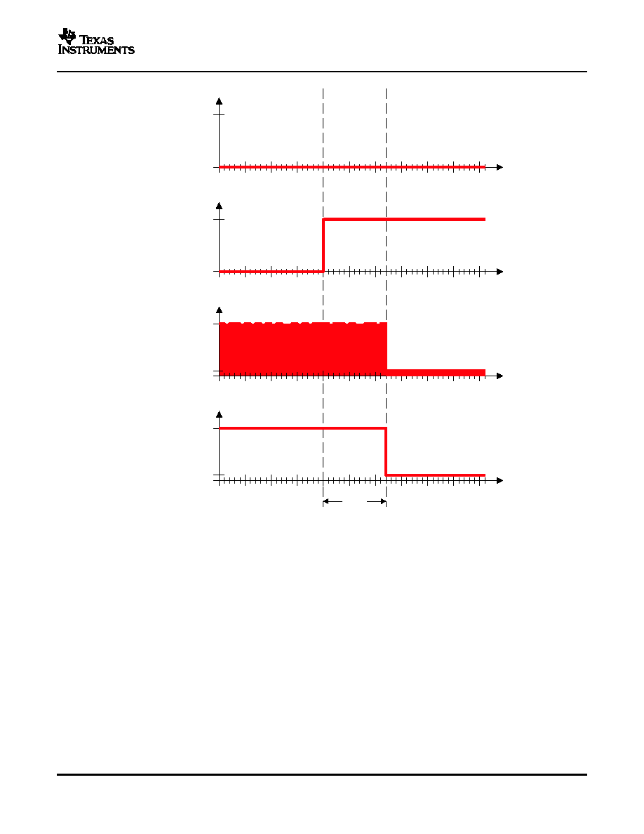
Figure 4. DISABLE Assert Time TOFF
11
www.ti.com
t
ON
t
t
t
t
V
HIGH
V
HIGH
I
MOD
I
BIAS
V
LOW
V
LOW
I
MOD-OFF
I
BIAS-OFF
SDOWN
DISABLE
I
MOD
I
BIAS
T0103-01
ONET4211LD
SLLS688 ≠ NOVEMBER 2005
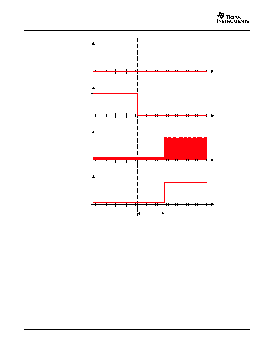
Figure 5. DISABLE Negate Time TON
12
www.ti.com
t
RESET
t
RESET
t
ON
t
t
t
t
V
HIGH
V
HIGH
I
MOD
I
BIAS
V
LOW
V
LOW
I
MOD-OFF
I
BIAS-OFF
SDOWN
DISABLE
I
MOD
I
BIAS
T0104-01
ONET4211LD
SLLS688 ≠ NOVEMBER 2005
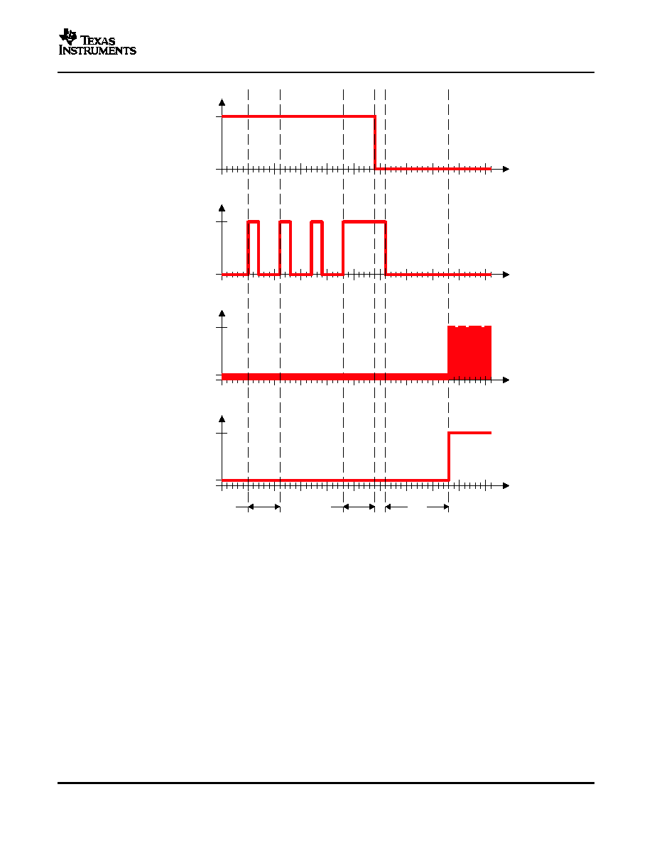
Figure 6. SDOWN Reset Time TRESET
13
www.ti.com
TYPICAL CHARACTERISTICS
Time [50ps/Div]
Single-Ended Output V
oltage
[50mV/Div]
G001
Time [100ps/Div]
Single-Ended Output V
oltage
[50mV/Div]
Time [100ps/Div]
Single-Ended Output V
oltage
[50mV/Div]
G002
Time [200ps/Div]
Single-Ended Output V
oltage
[50mV/Div]
Time [200ps/Div]
Single-Ended Output V
oltage
[50mV/Div]
G003
Modulation Current - mA
0
10
20
30
40
50
60
10
15
20
25
30
35
40
45
50
55
60
Deterministic Jitter Including PWD - ps
p
-
p
G004
ONET4211LD
SLLS688 ≠ NOVEMBER 2005
Typical operating condition is at V
CC
= 3.3 V, I
MOD
= 30 mA, I
BIAS
= 20 mA and T
A
= 25
∞
C (unless otherwise noted)
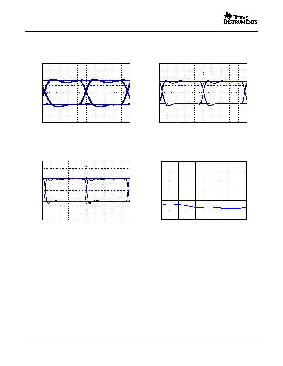
ELECTRICAL EYE-DIAGRAM AT 4.25 Gbps
ELECTRICAL EYE-DIAGRAM AT 2.125 Gbps
WITH K28.5 PATTERN
WITH K28.5 PATTERN
Figure 7.
Figure 8.
ELECTRICAL EYE-DIAGRAM AT 1.0625 Gbps
DETERMINISTIC JITTER
WITH K28.5 PATTERN
vs
MODULATION CURRENT
Figure 9.
Figure 10.
14
www.ti.com
Modulation Current - mA
0.0
0.5
1.0
1.5
2.0
2.5
3.0
10
15
20
25
30
35
40
45
50
55
60
Random Jitter - ps
R
M
S
G005
T
A
- Free-Air Temperature -
∞
C
0.0
0.5
1.0
1.5
2.0
2.5
3.0
-40 -30 -20 -10 0
10 20 30 40
50 60 70 80 90
Random Jitter - ps
R
M
S
G006
Modulation Current - mA
20
30
40
50
60
70
80
10
15
20
25
30
35
40
45
50
55
60
Rise T
ime and Fall T
ime - ps
G007
Fall Time
Rise Time
Bias Current - mA
10
11
12
13
14
15
16
17
18
19
20
10
15
20
25
30
35
40
45
50
55
60
Bias Monitor Current Gain - mA/A
G008
ONET4211LD
SLLS688 ≠ NOVEMBER 2005
TYPICAL CHARACTERISTICS (continued)
Typical operating condition is at V
CC
= 3.3 V, I
MOD
= 30 mA, I
BIAS
= 20 mA and T
A
= 25
∞
C (unless otherwise noted)
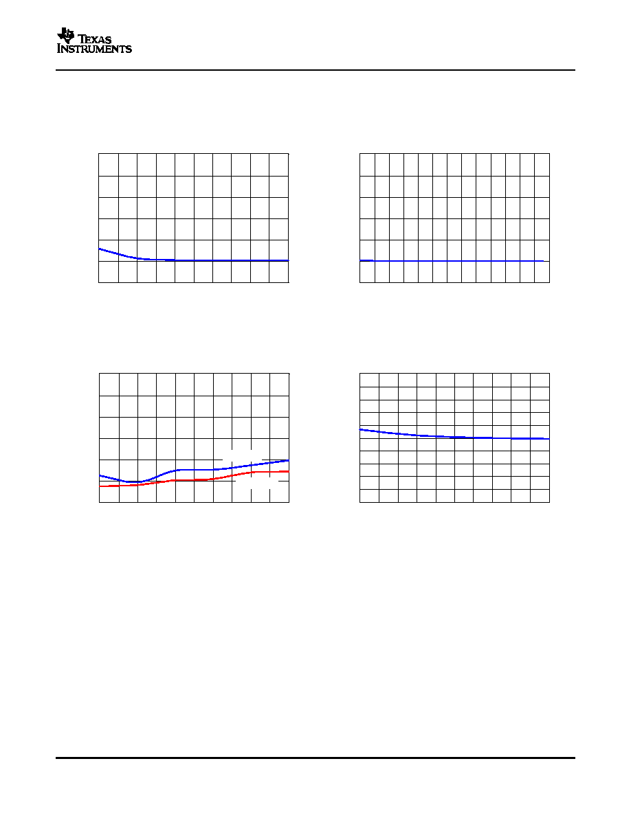
RANDOM JITTER
RANDOM JITTER
vs
vs
MODULATION CURRENT
TEMPERATURE
Figure 11.
Figure 12.
RISE TIME AND FALL TIME
BIAS-MONITOR CURRENT GAIN I
MONB
/I
BIAS
vs
vs
MODULATION CURRENT
BIAS CURRENT I
BIAS
Figure 13.
Figure 14.
15
www.ti.com
R
BIASMAX
- External Resistor - k
0
20
40
60
80
100
120
0
10
20
30
40
50
60
70
80
90
100
I
B
I
A
S
- Bias Current - mA
G009
R
MODSET
- External Resistor - k
0
10
20
30
40
50
60
70
80
90
100
0
10
20
30
40
50
60
70
80
90
100
I
M
O
D
- Modulation Current - mA
G010
R
APCSET
- External Resistor - k
0.0
0.2
0.4
0.6
0.8
1.0
1.2
1.4
1.6
1.8
0
10
20
30
40
50
60
70
80
90
100
I
P
D
- Monitor Diode Current - mA
G011
T
A
- Free-Air Temperature -
∞
C
0.0
0.5
1.0
1.5
2.0
2.5
3.0
-40 -30 -20 -10 0
10 20 30 40
50 60 70 80 90
Photodiode Monitor Gain - mA/mA
G012
ONET4211LD
SLLS688 ≠ NOVEMBER 2005
TYPICAL CHARACTERISTICS (continued)
Typical operating condition is at V
CC
= 3.3 V, I
MOD
= 30 mA, I
BIAS
= 20 mA and T
A
= 25
∞
C (unless otherwise noted)
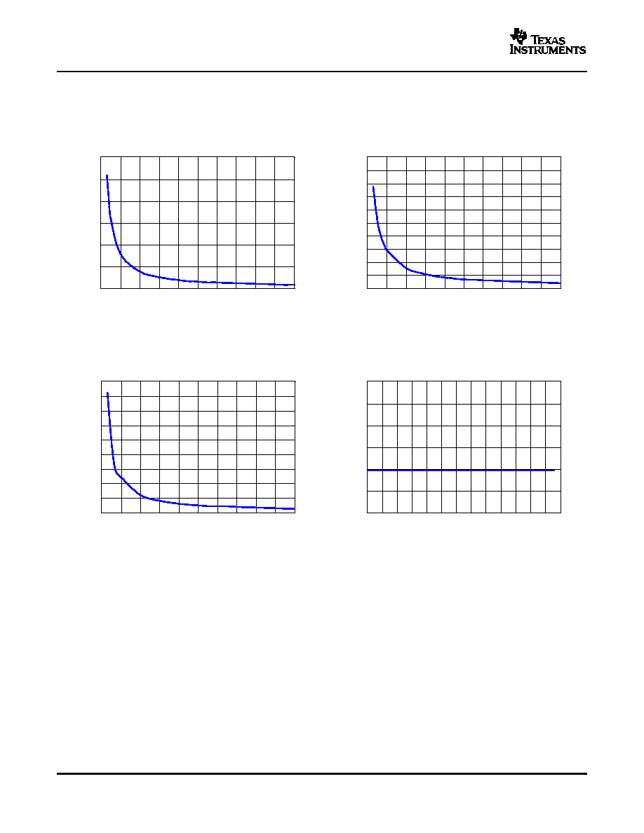
BIAS CURRENT I
BIAS
IN OPEN-LOOP MODE
MODULATION CURRENT I
MOD
vs
vs
EXTERNAL RESISTOR R
BIASMAX
EXTERNAL RESISTOR R
MODSET
Figure 15.
Figure 16.
MONITOR DIODE CURRENT I
PD
PHOTODIODE MONITOR GAIN I
MONP
/I
PD
vs
vs
EXTERNAL RESISTOR R
APCSET
TEMPERATURE
Figure 17.
Figure 18.
16

www.ti.com
T
A
- Free-Air Temperature -
∞
C
10
12
14
16
18
20
-40 -30 -20 -10 0
10 20 30 40
50 60 70 80 90
Bias Current Monitor Gain - mA/A
G013
T
A
- Free-Air Temperature -
∞
C
10
20
30
40
50
60
70
80
-40 -30 -20 -10 0
10 20 30 40
50 60 70 80 90
Supply Current - mA
G014
V
SDOWN
Time [500 ns/Div]
V
DISABLE
I
MOD+
I
BIAS
t = 2.15
µ
s
G016
T
A
- Free-Air Temperature -
∞
C
10
20
30
40
50
60
70
80
-40 -30 -20 -10 0
10 20 30 40
50 60 70 80 90
Modulation Current - mA
G015
R
MODTC
=
(Open)
R
MODTC
= 5.6 k
R
MODTC
= 3.1 k
V
SDOWN
V
DISABLE
I
MOD+
I
BIAS
t = 236
µ
s
G017
Time [100
µ
s/Div]
V
SDOWN
V
DISABLE
I
MOD+
I
BIAS
t = 12.8
µ
s
G018
Time [5
µ
s/Div]
ONET4211LD
SLLS688 ≠ NOVEMBER 2005
TYPICAL CHARACTERISTICS (continued)
Typical operating condition is at V
CC
= 3.3 V, I
MOD
= 30 mA, I
BIAS
= 20 mA and T
A
= 25
∞
C (unless otherwise noted)
BIAS CURRENT MONITOR GAIN I
MONB
/I
BIAS
SUPPLY CURRENT (excl. I
MOD
and I
BIAS
)
vs
vs
TEMPERATURE
TEMPERATURE
Figure 19.
Figure 20.
MODULATION CURRENT vs TEMPERATURE
DISABLE ASSERT TIME T
OFF
FOR DIFFERENT SETTINGS OF R
MODTC
Figure 21.
Figure 22.
DISABLE NEGATE TIME T
ON
SHUTDOWN RESET TIME T
RESET
Figure 23.
Figure 24.
17

www.ti.com
APPLICATION INFORMATION
S0154-01
ONET4211LD
24-Lead QFN
Monitor
Photodiode
Laser
Diode
GND
VCC
MOD
!
MOD+
VCC
BIAS
DISABLE
APCSET
OUTPOL
IBMAX
CAPC
PD
GND
R
APC
SET
R
BI
ASMAX
R
MO
N
P
R
MO
N
B
R
MO
D
SET
R
MO
N
T
C
C
APC
VCC
DIN+
20 W
R
D
DIN
!
VCC
GND
MONP
MONB
SDOWN
FL
TMODE
MODSET
MODTC
DISABLE
VCC
FLTMODE
SDOWN
DIN+
DIN
!
MONP
MONB
OUTPOL
ONET4211LD
SLLS688 ≠ NOVEMBER 2005
Figure 25
shows the ONET4211LD connected with a dc-coupled interface to the laser diode; alternatively, the
ONET4211LD laser driver can be ac-coupled.
Figure 25. Basic Application Circuit With DC-Coupled Interface Between
the ONET4211LD and the Laser Diode
APC loop instability can occur with large inductive loading on the BIAS pin. To ensure loop stability in this case, it
is recommended to connect a 1-nF capacitor to ground at the BIAS pin.
18
www.ti.com
SELECT A LASER
SELECT APCSET RESISTOR
I
PD
[A]
+
P
AVG
[W]
Ú
MON
[A W]
(7)
R
APCSET
[
W
]
+
4.69 V
I
PD
[A]
+
4.69 V
P
AVG
[W]
Ú
MON
[A W]
(8)
R
APCSET
[
W
]
+
4.69 V
P
AVG
[W]
Ú
MON
[A W]
+
4.69 V
5 mW
0.05 mA mW
+
18.75 k
W
(9)
SELECT MODSET RESISTOR
I
MOD
[A]
+
Pp
*
p[W]
h
[W A]
+
2
P
AVG
[W]
re
*
1
re
)
1
h
[W A]
(10)
I
MOD
+
2
5 mW
6.3
*
1
6.3
)
1
0.2 mW mA
+
36.3 mA
(11)
I
MOD
[A]
+
I
MOD0
[A]
1
)
TC
T[
o
C]
*
T
0
[
o
C]
(12)
ONET4211LD
SLLS688 ≠ NOVEMBER 2005
APPLICATION INFORMATION (continued)
In the design example according to
Figure 25
, the ONET4211LD is dc-coupled to a typical communication-grade
laser diode capable of operating at 4.25 Gb/s with the following specifications shown in
Table 2
.
Table 2. Laser Diode Specifications
PARAMETER
VALUE
UNITS
Wavelength
1310
nm
P
AVG
Average Optical Output Power
5
mW
I
TH
Threshold current
10
mA
MON
Laser-to-monitor transfer
0.05
mA/mW
Laser slope efficiency
0.2
mW/mA
When the APC loop is activated, the desired average optical output power P
AVG
is defined by characteristics of
the monitor diode and by the APCSET resistor R
APCSET
. The relation between the monitor photodiode current I
PD
and the average optical output power P
AVG
is given by
Equation 7
:
The R
APCSET
resistor is calculated by
Equation 8
:
For the laser diode specified in
Table 2
and the desired average optical output power of 5 mW, R
APCSET
is
calculated as in
Equation 9
:
Note that the monitor photodiode current I
PD
must not exceed 1.5 mA, corresponding to a minimum APCSET
resistor R
APCSET,MIN
= 3.1 k
.
Modulation current I
MOD
is dependent on the required optical output peak-to-peak power P
p-p
or the average
optical power P
AVG
. I
MOD
can be calculated using the laser slope efficiency
and the desired extinction ratio r
e
:
Using the laser diode parameters from
Table 2
and assuming an extinction ratio r
e
= 8 dB (
6.3) for an average
optical power P
AVG
= 5 mW, the required modulation current results as:
The modulation current is adjustable, with a selectable temperature coefficient TC according to the relation:
where T is the ambient temperature in
∞
C and T
0
is the reference temperature (T
0
= 60
∞
C).
The temperature coefficient TC of the modulation current is typically adjustable between 630 ppm/
∞
C and 8300
ppm/
∞
C.
For calculation of the required external resistor R
MODSET
for a given modulation current and a given temperature,
the formula can be modified as follows:
19

www.ti.com
R
MODSET
[
W
]
+
265 V
I
MOD
[A]
1
)
TC
T[
o
C]
*
T
0
[
o
C]
(13)
R
MODSET
[
W
]
+
265 V
36.3 mA
1
)
4000 ppm
o
C
(25
o
C
*
60
o
C)
+
6.3 k
W
(14)
SELECT MODTC RESISTOR
TC
LD
1
o
C
+
h
2
[W A]
* h
1
[W A]
h
1
[W A]
T
2
[
o
C]
*
T
1
[
o
C]
10
6
(15)
TC
LD
+
0.15 mW mA
*
0.2 mW mA
0.2 mW mA
(85
o
C
*
25
o
C)
10
6
+ *
4167 1
o
C
(16)
R
MODTC
+
24
W
(TC
*
630 ppm)
1
o
C
o
C
(17)
R
MODTC
+
24
W
4167 ppm
*
630 ppm
o
C
o
C
+
6.8 k
W
(18)
SELECT BIASMAX RESISTOR
I
BIASMAX
[A]
+
I
THMAX
[A]
(19)
R
BIASMAX
[
W
]
+
343 V
I
BIASMAX
[A]
+
343 V
I
THMAX
[A]
(20)
ONET4211LD
SLLS688 ≠ NOVEMBER 2005
If 4000 ppm/
∞
C is the desired temperature coefficient and the modulation current from the preceding example,
36.3 mA, is required at a temperature of 25
∞
C, the MODSET resistor R
MODSET
is given by
Equation 14
.
Note that the modulation current I
MOD
must not exceed 85 mA over the complete temperature range,
corresponding to a minimum MODSET resistor R
MODSET,MIN
= 3.1 k
.
The R
MODTC
resistor is used to program a modulation temperature coefficient that can be used to compensate for
the decreased slope efficiency of the laser at a higher temperature. The temperature coefficient TC
LD
of the laser
can be calculated using the slope efficiency
1
at temperature T
1
and
2
at temperature T
2
as shown in
Equation 15
:
As an example, for the laser in
Table 2
, the slope efficiency at temperature T
1
= 25
∞
C is
1
= 0.2 mW/mA. At
temperature T
2
= 85
∞
C, the slope efficiency is
2
= 0.15 mW/mA. The corresponding temperature coefficient
TC
LD
of the laser can be calculated:
The MODTC resistor R
MODTC
can be used to compensate the laser temperature coefficient TC
LD
in order to
maintain the same optical output swing within a range of 630 ppm up to 8300 ppm. For this, R
MODTC
may be
programmed as follows:
To compensate for the decreased slope efficiency of the laser in
Table 2
, TC must be 4167 ppm/
∞
C.
This leads to the following MODTC resistor R
MODTC
:
The BIASMAX resistor R
BIASMAX
is used to limit the bias current applied to the laser diode.
To calculate R
BIASMAX
, the maximum threshold current at 85
∞
C and end of life must be determined. The
maximum bias current for the dc-coupled interface can be approximated by
Equation 19
.
R
BIASMAX
can be set by
Equation 20
.
For the example laser diode, the maximum threshold current is 40 mA at 85
∞
C. Therefore, R
BIASMAX
can be
approximated by
Equation 21
.
20

www.ti.com
R
BIASMAX
+
343 V
40 mA
+
8.6 k
W
(21)
SELECT V
MONB
AND V
MONP
RANGE
V
MONB
[V]
+
R
MONB
[
W
]
I
BIAS
[A]
68
+
768
W
I
BIAS
[A]
68
+
11.29
W
I
BIAS
[A]
(22)
V
MONP
[V]
+
R
MONP
[
W
]
I
PD
[A]
+
200
W
I
PD
[A]
(23)
LASER DIODE INTERFACE
ONET4211LD
SLLS688 ≠ NOVEMBER 2005
Monitoring the bias current is achieved by taking the fractional (1/68) bias current and developing a voltage
across an external resistor to ground.
Equation 22
provides the value for V
MONB
for a resistor value equal to
768
.
Monitoring of the photo current is achieved by taking a mirror of I
PD
and developing a voltage across an external
resistor to ground.
Equation 23
provides the value for V
MONP
for a resistor equal to 200
.
The output stage of the ONET4211LD is optimized for driving a 20-
load. The combination of a damping
resistor, R
D
, along with the resistance of the laser diode, must be 20
for impedance matching. The suggested
typical value for R
D
is 6
to 15
. A bypass capacitor of 10 nF placed close to the laser anode also helps to
optimize performance.
21

PACKAGING INFORMATION
Orderable Device
Status
(1)
Package
Type
Package
Drawing
Pins Package
Qty
Eco Plan
(2)
Lead/Ball Finish
MSL Peak Temp
(3)
ONET4211LDRGER
ACTIVE
QFN
RGE
24
3000 Green (RoHS &
no Sb/Br)
CU NIPDAU
Level-2-260C-1 YEAR
ONET4211LDRGET
ACTIVE
QFN
RGE
24
250
Green (RoHS &
no Sb/Br)
CU NIPDAU
Level-2-260C-1 YEAR
(1)
The marketing status values are defined as follows:
ACTIVE: Product device recommended for new designs.
LIFEBUY: TI has announced that the device will be discontinued, and a lifetime-buy period is in effect.
NRND: Not recommended for new designs. Device is in production to support existing customers, but TI does not recommend using this part in
a new design.
PREVIEW: Device has been announced but is not in production. Samples may or may not be available.
OBSOLETE: TI has discontinued the production of the device.
(2)
Eco
Plan
-
The
planned
eco-friendly
classification:
Pb-Free
(RoHS)
or
Green
(RoHS
&
no
Sb/Br)
-
please
check
http://www.ti.com/productcontent
for the latest availability information and additional product content details.
TBD: The Pb-Free/Green conversion plan has not been defined.
Pb-Free (RoHS): TI's terms "Lead-Free" or "Pb-Free" mean semiconductor products that are compatible with the current RoHS requirements
for all 6 substances, including the requirement that lead not exceed 0.1% by weight in homogeneous materials. Where designed to be soldered
at high temperatures, TI Pb-Free products are suitable for use in specified lead-free processes.
Green (RoHS & no Sb/Br): TI defines "Green" to mean Pb-Free (RoHS compatible), and free of Bromine (Br) and Antimony (Sb) based flame
retardants (Br or Sb do not exceed 0.1% by weight in homogeneous material)
(3)
MSL, Peak Temp. -- The Moisture Sensitivity Level rating according to the JEDEC industry standard classifications, and peak solder
temperature.
Important Information and Disclaimer:The information provided on this page represents TI's knowledge and belief as of the date that it is
provided. TI bases its knowledge and belief on information provided by third parties, and makes no representation or warranty as to the
accuracy of such information. Efforts are underway to better integrate information from third parties. TI has taken and continues to take
reasonable steps to provide representative and accurate information but may not have conducted destructive testing or chemical analysis on
incoming materials and chemicals. TI and TI suppliers consider certain information to be proprietary, and thus CAS numbers and other limited
information may not be available for release.
In no event shall TI's liability arising out of such information exceed the total purchase price of the TI part(s) at issue in this document sold by TI
to Customer on an annual basis.
PACKAGE OPTION ADDENDUM
www.ti.com
18-Nov-2005
Addendum-Page 1

IMPORTANT NOTICE
Texas Instruments Incorporated and its subsidiaries (TI) reserve the right to make corrections, modifications,
enhancements, improvements, and other changes to its products and services at any time and to discontinue
any product or service without notice. Customers should obtain the latest relevant information before placing
orders and should verify that such information is current and complete. All products are sold subject to TI's terms
and conditions of sale supplied at the time of order acknowledgment.
TI warrants performance of its hardware products to the specifications applicable at the time of sale in
accordance with TI's standard warranty. Testing and other quality control techniques are used to the extent TI
deems necessary to support this warranty. Except where mandated by government requirements, testing of all
parameters of each product is not necessarily performed.
TI assumes no liability for applications assistance or customer product design. Customers are responsible for
their products and applications using TI components. To minimize the risks associated with customer products
and applications, customers should provide adequate design and operating safeguards.
TI does not warrant or represent that any license, either express or implied, is granted under any TI patent right,
copyright, mask work right, or other TI intellectual property right relating to any combination, machine, or process
in which TI products or services are used. Information published by TI regarding third-party products or services
does not constitute a license from TI to use such products or services or a warranty or endorsement thereof.
Use of such information may require a license from a third party under the patents or other intellectual property
of the third party, or a license from TI under the patents or other intellectual property of TI.
Reproduction of information in TI data books or data sheets is permissible only if reproduction is without
alteration and is accompanied by all associated warranties, conditions, limitations, and notices. Reproduction
of this information with alteration is an unfair and deceptive business practice. TI is not responsible or liable for
such altered documentation.
Resale of TI products or services with statements different from or beyond the parameters stated by TI for that
product or service voids all express and any implied warranties for the associated TI product or service and
is an unfair and deceptive business practice. TI is not responsible or liable for any such statements.
Following are URLs where you can obtain information on other Texas Instruments products and application
solutions:
Products
Applications
Amplifiers
amplifier.ti.com
Audio
www.ti.com/audio
Data Converters
dataconverter.ti.com
Automotive
www.ti.com/automotive
DSP
dsp.ti.com
Broadband
www.ti.com/broadband
Interface
interface.ti.com
Digital Control
www.ti.com/digitalcontrol
Logic
logic.ti.com
Military
www.ti.com/military
Power Mgmt
power.ti.com
Optical Networking
www.ti.com/opticalnetwork
Microcontrollers
microcontroller.ti.com
Security
www.ti.com/security
Telephony
www.ti.com/telephony
Video & Imaging
www.ti.com/video
Wireless
www.ti.com/wireless
Mailing Address:
Texas Instruments
Post Office Box 655303 Dallas, Texas 75265
Copyright
2005, Texas Instruments Incorporated