Æ
OPA124
1
FEATURES
q
LOW NOISE: 6nV/
Hz (10kHz)
q
LOW BIAS CURRENT: 1pA max
q
LOW OFFSET: 250
µ
V max
q
LOW DRIFT: 2
µ
V/
∞
C max
q
HIGH OPEN-LOOP GAIN: 120dB min
q
HIGH COMMON-MODE REJECTION:
100dB min
q
AVAILABLE IN 8-PIN PLASTIC DIP
AND 8-PIN SOIC PACKAGES
APPLICATIONS
q
PRECISION PHOTODIODE PREAMP
q
MEDICAL EQUIPMENT
q
OPTOELECTRONICS
q
DATA ACQUISITION
q
TEST EQUIPMENT
OPA124
DESCRIPTION
The OPA124 is a precision monolithic FET opera-
tional amplifier using a
Difet
(dielectrical isolation)
manufacturing process. Outstanding DC and AC per-
formance characteristics allow its use in the most
critical instrumentation applications.
Bias current, noise, voltage offset, drift, open-loop
gain, common-mode rejection and power supply re-
jection are superior to BIFET and CMOS amplifiers.
Difet
fabrication achieves extremely low input bias
currents without compromising input voltage noise
performance. Low input bias current is maintained
over a wide input common-mode voltage range with
unique cascode circuitry. This cascode design also
allows high precision input specifications and reduced
susceptibility to flicker noise. Laser trimming of thin-
film resistors gives very low offset and drift.
Compared to the popular OPA111, the OPA124 gives
comparable performance and is available in an 8-pin
PDIP and 8-pin SOIC package.
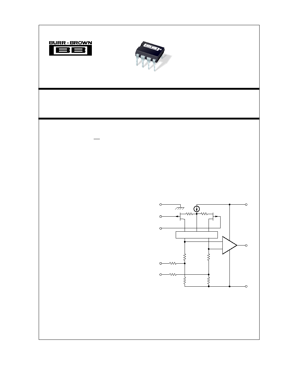
BIFET
Æ
National Semiconductor Corp.,
Difet
Æ
Burr-Brown Corp.
Æ
Low Noise Precision
Difet
Æ
OPERATIONAL AMPLIFIER
8
2
3
1
5
7
6
4
Substrate
Output
Trim
(1)
+V
CC
Noise-Free Cascode
(2)
Trim
(1)
+In
≠In
≠V
CC
2k
2k
2k
10k
10k
NOTES: (1) Omitted on SOIC. (2) Patented.
2k
OPA124 Simplified Circuit
International Airport Industrial Park ∑ Mailing Address: PO Box 11400, Tucson, AZ 85734 ∑ Street Address: 6730 S. Tucson Blvd., Tucson, AZ 85706 ∑ Tel: (520) 746-1111 ∑ Twx: 910-952-1111
Internet: http://www.burr-brown.com/ ∑ FAXLine: (800) 548-6133 (US/Canada Only) ∑ Cable: BBRCORP ∑ Telex: 066-6491 ∑ FAX: (520) 889-1510 ∑ Immediate Product Info: (800) 548-6132
© 1993 Burr-Brown Corporation
PDS-1203C
Printed in U.S.A. March, 1998
OPA124
SBOS028

Æ
OPA124
2
SPECIFICATIONS
ELECTRICAL
At V
CC
=
±
15VDC and T
A
= +25
∞
C, unless otherwise noted.
OPA124U, P
OPA124UA, PA
OPA124PB
PARAMETER
CONDITION
MIN
TYP
MAX
MIN
TYP
MAX
MIN
TYP
MAX
UNITS
INPUT NOISE
Voltage, f
O
= 10Hz
(4)
40
80
T
T
T
T
nV/
Hz
f
O
= 100Hz
(4)
15
40
T
T
T
T
nV/
Hz
f
O
= 1kHz
(4)
8
15
T
T
T
T
nV/
Hz
f
O
= 10kHz
(5)
6
8
T
T
T
T
nV/
Hz
f
B
= 10Hz to 10kHz
(5)
0.7
1.2
T
T
T
T
µ
Vrms
f
B
= 0.1Hz to 10Hz
1.6
3.3
T
T
T
T
µ
Vp-p
Current, f
B
= 0.1Hz to 10Hz
9.5
15
T
T
T
T
fAp-p
f
O
= 0.1Hz thru 20kHz
0.5
0.8
T
T
T
T
fA/
Hz
OFFSET VOLTAGE
(1)
Input Offset Voltage
V
CM
= 0VDC
±
200
±
800
±
150
±
500
±
100
±
250
µ
V
vs Temperature
T
A
= T
MIN
to T
MAX
±
4
±
7.5
±
2
±
4
±
1
±
2
µ
V/
∞
C
Supply Rejection
V
CC
=
±
10V to
±
18V
88
110
90
T
100
T
dB
vs Temperature
T
A
= T
MIN
to T
MAX
84
100
86
T
90
T
dB
BIAS CURRENT
(1)
Input Bias Current
V
CM
= 0VDC
±
1
±
5
±
0.5
±
2
±
0.35
±
1
pA
OFFSET CURRENT
(1)
Input Offset Current
V
CM
= 0VDC
±
1
±
5
±
0.5
±
1
±
0.25
±
0.5
pA
IMPEDANCE
Differential
10
13
|| 1
T
T
|| pF
Common-Mode
10
14
|| 3
T
T
|| pF
VOLTAGE RANGE
Common-Mode Input Range
±
10
±
11
T
T
T
T
V
Common-Mode Rejection
V
IN
=
±
10VDC
92
110
94
T
100
T
dB
vs Temperature
T
A
= T
MIN
to T
MAX
86
100
T
T
90
T
dB
OPEN-LOOP GAIN, DC
Open-Loop Voltage Gain
R
L
2k
106
125
T
T
120
T
dB
FREQUENCY RESPONSE
Unity Gain, Small Signal
1.5
T
T
MHz
Full Power Response
20Vp-p, R
L
= 2k
16
32
T
T
T
T
kHz
Slew Rate
V
O
=
±
10V, R
L
= 2k
1
1.6
T
T
T
T
V/
µ
s
THD
0.0003
T
T
%
Settling Time, 0.1%
Gain = ≠1, R
L
= 2k
6
T
T
µ
s
0.01%
10V Step
10
T
T
µ
s
Overload Recovery,
50% Overdrive
(2)
Gain = ≠1
5
T
T
µ
s
RATED OUTPUT
Voltage Output
R
L
= 2k
±
11
±
12
T
T
T
T
V
Current Output
V
O
=
±
10VDC
±
5.5
±
10
T
T
T
T
mA
Output Resistance
DC, Open Loop
100
T
T
Load Capacitance Stability
Gain = +1
1000
T
T
pF
Short Circuit Current
10
40
T
T
T
T
mA
POWER SUPPLY
Rated Voltage
±
15
T
T
VDC
Voltage Range, Derated
±
5
±
18
T
T
T
T
VDC
Current, Quiescent
I
O
= 0mADC
2.5
3.5
T
T
T
T
mA
TEMPERATURE RANGE
Specification
T
MIN
and T
MAX
≠25
+85
T
T
T
T
∞
C
Storage
≠65
+125
T
T
T
T
∞
C
Junction-Ambient: PDIP
90
T
T
∞
C/W
SOIC
100
T
T
∞
C/W
T
Specification same as OPA124U, P
NOTES: (1) Offset voltage, offset current, and bias current are measured with the units fully warmed up. For performance at other temperatures see Typical Performance
Curves. (2) Overload recovery is defined as the time required for the output to return from saturation to linear operation following the removal of a 50% input overdrive.
(3) For performance at other temperatures see Typical Performance Curves. (4) Sample tested, 98% confidence. (5) Guaranteed by design.

Æ
OPA124
3
CONNECTION DIAGRAMS
Top View
DIP
1
2
3
4
8
7
6
5
Substrate
+V
S
Output
Offset Trim
Offset Trim
≠In
+In
≠V
S
Top View
SOIC
1
2
3
4
8
7
6
5
Substrate
+V
S
Output
NC
NC
≠In
+In
≠V
S
NC = No Connect
The information provided herein is believed to be reliable; however, BURR-BROWN assumes no responsibility for inaccuracies or omissions. BURR-BROWN assumes
no responsibility for the use of this information, and all use of such information shall be entirely at the user's own risk. Prices and specifications are subject to change
without notice. No patent rights or licenses to any of the circuits described herein are implied or granted to any third party. BURR-BROWN does not authorize or warrant
any BURR-BROWN product for use in life support devices and/or systems.
PACKAGE/ORDERING INFORMATION
BIAS
OFFSET
PACKAGE
TEMPERATURE
CURRENT
DRIFT
PRODUCT
PACKAGE
DRAWING NUMBER
(1)
RANGE
pA, max
µ
V/
∞
C, max
OPA124U
8-Lead SOIC
182
≠25
∞
C to +85
∞
C
5
7.5
OPA124P
8-Pin Plastic DIP
006
≠25
∞
C to +85
∞
C
5
7.5
OPA124UA
8-Lead SOIC
182
≠25
∞
C to +85
∞
C
2
4
OPA124PA
8-Pin Plastic DIP
006
≠25
∞
C to +85
∞
C
2
4
OPA124PB
8-Pin Plastic DIP
006
≠25
∞
C to +85
∞
C
1
2
NOTE: (1) For detailed drawing and dimension table, please see end of data sheet, or Appendix C of Burr-Brown IC Data Book.
ABSOLUTE MAXIMUM RATINGS
(1)
Supply ...........................................................................................
±
18VDC
Internal Power Dissipation
(2)
......................................................... 750mW
Differential Input Voltage
(3)
..........................................................
±
36VDC
Input Voltage Range
(3)
.................................................................
±
18VDC
Storage Temperature Range .......................................... ≠65
∞
C to +150
∞
C
Operating Temperature Range ....................................... ≠40
∞
C to +125
∞
C
Lead Temperature (soldering, 10s) ................................................ +300
∞
C
Output Short Circuit Duration
(4)
............................................... Continuous
Junction Temperature .................................................................... +175
∞
C
NOTES: (1) Stresses above these ratings may cause permanent damage.
(2) Packages must be derated based on
JA
= 90
∞
C/W for PDIP and 100
∞
C/W
for SOIC. (3) For supply voltages less than
±
18VDC, the absolute maximum
input voltage is equal to +18V > V
IN
> ≠V
CC
≠ 6V. See Figure 2. (4) Short circuit
may be to power supply common only. Rating applies to +25
∞
C ambient.
Observe dissipation limit and T
J
.
ELECTROSTATIC
DISCHARGE SENSITIVITY
This integrated circuit can be damaged by ESD. Burr-Brown
recommends that all integrated circuits be handled with
appropriate precautions. Failure to observe proper handling
and installation procedures can cause damage.
ESD damage can range from subtle performance degrada-
tion to complete device failure. Precision integrated circuits
may be more susceptible to damage because very small
parametric changes could cause the device not to meet its
published specifications.
Æ
OPA124
4
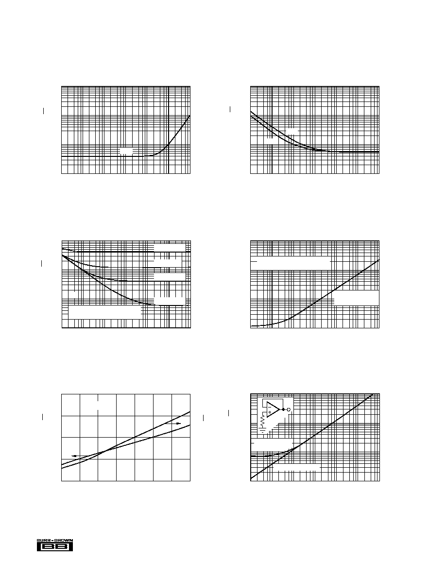
VOLTAGE AND CURRENT NOISE SPECTRAL
DENSITY vs TEMPERATURE
12
10
8
6
4
≠50
≠25
0
25
50
75
100
125
Temperature (∞C)
100
10
1
0.1
0.01
f
O
= 1kHz
Voltage Noise (nV/
Hz)
Current Noise (fA/
Hz)
TYPICAL PERFORMANCE CURVES
At T
A
= +25
∞
C, and V
CC
=
±
15VDC, unless otherwise noted.
INPUT CURRENT NOISE SPECTRAL DENSITY
1k
Frequency (Hz)
100
10
1
10k
100k
1M
100
10
1
0.1
Current Noise (fA/
Hz)
PB
INPUT VOLTAGE NOISE SPECTRAL DENSITY
1k
Frequency (Hz)
10k
100k
1M
100
10
1
1k
100
10
1
U, P
PB
Voltage Noise (nV/
Hz)
TOTAL
(1)
INPUT VOLTAGE NOISE SPECTRAL
DENSITY vs SOURCE RESISTANCE
100
Frequency (Hz)
1k
10k
100k
10
1
0.1
1k
100
10
1
R
S
= 10M
R
S
= 1M
R
S
= 100k
R
S
= 100
PB
NOTE: (1) Includes contribution
from source resistance.
Voltage Noise (nV/
Hz)
TOTAL
(1)
INPUT VOLTAGE NOISE (PEAK-TO-PEAK)
vs SOURCE RESISTANCE
10
1k
100
10
1
Voltage Noise (µVp-p)
NOTE: (1) Includes contribution
from source resistance.
4
Source Resistance (
)
10
5
10
6
10
7
10
8
10
9
10
10
PB
f
B
= 0.1Hz to 10Hz
TOTAL INPUT VOLTAGE NOISE SPECTRAL DENSITY
AT 1kHz vs SOURCE RESISTANCE
1k
100
10
1
100
1k
10k
100k
1M
10M
100M
Source Resistance ( )
Resistor Noise Only
OPA124PB +
Resistor
E
O
R
S
Voltage Noise, E
O
(nV/
Hz)
Æ
OPA124
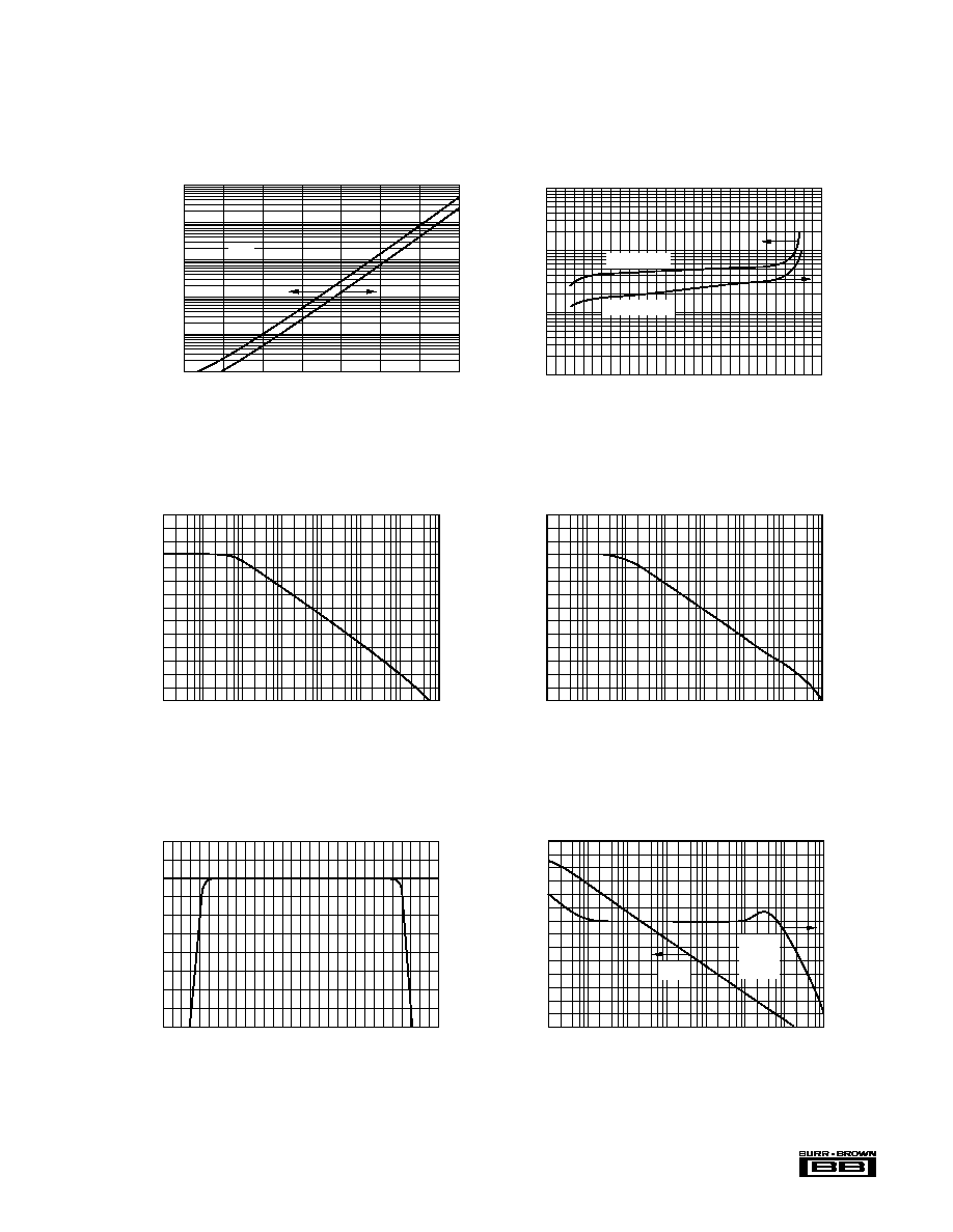
5
COMMON-MODE REJECTION
vs INPUT COMMON-MODE VOLTAGE
≠15
Common-Mode Voltage (V)
≠10
≠5
0
5
10
15
Common-Mode Rejection (dB)
120
110
100
90
80
70
BIAS AND OFFSET CURRENT
vs INPUT COMMON-MODE VOLTAGE
≠15
≠10
≠5
0
5
10
15
10
1
0.1
0.01
Bias Current (pA)
10
1
0.1
0.01
Offset Current (pA)
Common-Mode Voltage (V)
Bias Current
Offset Current
OPEN-LOOP FREQUENCY RESPONSE
1
Frequency (Hz)
10
100
1k
10k
100k
1M
10M
Voltage Gain (dB)
140
120
100
80
60
40
20
0
Phase
Margin
65∞
≠45
≠90
≠135
≠180
Phase Shift (Degrees)
Gain
COMMON-MODE REJECTION
vs FREQUENCY
1
Frequency (Hz)
10
100
1k
10k
100k
1M
10M
Common-Mode Rejection (dB)
140
120
100
80
60
40
20
0
POWER SUPPLY REJECTION
vs FREQUENCY
1
Frequency (Hz)
10
100
1k
10k
100k
1M
10M
Power Supply Rejection (dB)
140
120
100
80
60
40
20
0
TYPICAL PERFORMANCE CURVES
(CONT)
At T
A
= +25
∞
C, and V
CC
=
±
15VDC, unless otherwise noted.
BIAS AND OFFSET CURRENT
vs TEMPERATURE
≠50
Ambient Temperature (∞C)
≠25
0
25
50
75
100
125
1k
100
10
1
0.1
0.01
Bias Current (pA)
PB
1k
100
10
1
0.1
0.01
Offset Current (pA)
Æ
OPA124
6
SMALL SIGNAL TRANSIENT RESPONSE
1
Time (µs)
0
5
60
40
20
0
≠20
≠40
≠60
Output Voltage (mV)
2
3
4
LARGE SIGNAL TRANSIENT RESPONSE
10
Time (µs)
0
50
15
10
5
0
≠5
≠10
≠15
Output Voltage (V)
20
30
40
MAXIMUM UNDISTORTED OUTPUT
VOLTAGE vs FREQUENCY
100k
Frequency (Hz)
1k
10k
1M
30
20
10
0
Output Voltage (Vp-p)
OPEN-LOOP GAIN vs TEMPERATURE
140
130
120
110
100
≠50
≠25
0
25
50
75
100
125
Ambient Temperature (∞C)
Voltage Gain (dB)
GAIN-BANDWIDTH AND SLEW RATE
vs SUPPLY VOLTAGE
Gain Bandwidth (MHz)
0
3
2
1
0
Slew Rate (V/µs)
3
2
1
0
5
10
15
20
Supply Voltage (±V
CC
)
GAIN-BANDWIDTH AND SLEW RATE
vs TEMPERATURE
4
3
2
1
0
≠50
≠25
0
25
50
75
100
125
Ambient Temperature (∞C)
Gain Bandwidth (MHz)
4
3
2
1
0
Slew Rate (V/µs)
4
3
2
1
0
TYPICAL PERFORMANCE CURVES
(CONT)
At T
A
= +25
∞
C, and V
CC
=
±
15VDC, unless otherwise noted.

Æ
OPA124
7
INPUT OFFSET VOLTAGE WARM-UP DRIFT
20
10
0
≠10
≠20
Time From Power Turn-On (Minutes)
Offset Voltage Change (µV)
0
1
2
3
4
5
6
SUPPLY CURRENT vs TEMPERATURE
4
3
2
1
0
≠50
≠25
0
25
50
75
100
125
Ambient Temperature (∞C)
Supply Current (mA)
SETTLING TIME vs CLOSED-LOOP GAIN
1
Closed-Loop Gain (V/V)
10
100
1k
100
80
60
40
20
0
Settling Time (µs)
0.1%
0.01%
TYPICAL PERFORMANCE CURVES
(CONT)
At T
A
= +25
∞
C, and V
CC
=
±
15VDC, unless otherwise noted.
INPUT OFFSET VOLTAGE CHANGE
DUE TO THERMAL SHOCK
150
75
0
≠75
≠150
Time From Thermal Shock (Minutes)
Offset Voltage Change (µV)
≠1
0
1
2
3
4
5
+25∞C
+85∞C
PB
U, P
T
A
= +25∞C to T
A
= +85∞C
Air Environment

Æ
OPA124
8
APPLICATIONS INFORMATION
OFFSET VOLTAGE ADJUSTMENT
The OPA124 offset voltage is laser-trimmed and will require
no further trim for most applications. In order to reduce
layout leakage errors, the offset adjust capability has been
removed from the SOIC versions (OPA124UA and
OPA124U). The PDIP versions (OPA124PB, OPA124PA,
and OPA124P) do have pins available for offset adjustment.
As with most amplifiers, externally trimming the remaining
offset can change drift performance by about 0.3
µ
V/
∞
C for
each 100
µ
V of adjusted offset. The correct circuit configu-
ration for offset adjust for the PDIP packages is shown in
Figure 1.
INPUT PROTECTION
Conventional monolithic FET operational amplifiers require
external current-limiting resistors to protect their inputs
against destructive currents that can flow when input FET
gate-to-substrate isolation diodes are forward-biased. Most
BIFET amplifiers can be destroyed by the loss of ≠V
CC
.
Unlike BIFET amplifiers, the
Difet
OPA124 requires input
current limiting resistors only if its input voltage is greater
than 6V more negative than ≠V
CC
. A 10k
series resistor
will limit input current to a safe level with up to
±
15V input
levels, even if both supply voltages are lost (Figure 2).
Static damage can cause subtle changes in amplifier input
characteristics without necessarily destroying the device. In
precision operational amplifiers (both bipolar and FET types),
this may cause a noticeable degradation of offset voltage and
drift. Static protection is recommended when handling any
precision IC operational amplifier.
GUARDING AND SHIELDING
As in any situation where high impedances are involved,
careful shielding is required to reduce "hum" pickup in input
leads. If large feedback resistors are used, they should also
be shielded along with the external input circuitry.
Leakage currents across printed circuit boards can easily
exceed the bias current of the OPA124. To avoid leakage
problems, the OPA124 should be soldered directly into a
printed circuit board. Utmost care must be used in planning
the board layout. A "guard" pattern should completely
surround the high impedance input leads and should be
connected to a low impedance point which is at the signal
input potential.
The amplifier substrate should be connected to any input
shield or guard via pin 8 minimizing both leakage and noise
pickup (see Figure 3).
If guarding is not required, pin 8 should be connected to
ground.
OPA124P
2
3
7
+V
CC
4
5
1
6
≠V
CC
10k
(100k
to 1M
trim potentiometer.
±10mV typical trim range.
recommended).
NOTE: No trim on SOIC.
FIGURE 3. Connection of Input Guard.
FIGURE 2. Input Current vs Input Voltage with
±
V
CC
Pins
Grounded.
V
I
IN
Maximum Safe Current
Maximum Safe Current
≠15
Input Voltage (V)
≠10
≠5
0
5
10
15
Input Current (mA)
2
1
0
≠1
≠2
FIGURE 1. Offset Voltage Trim for PDIP packages.
4
OPA124
2
3
6
8
In
Out
Inverting
OPA124
2
3
6
In
Out
Non-Inverting
8
OPA124
2
3
6
In
Out
Buffer
8
Board layout for PDIP input guarding: guard top and bottom of board.
Bottom View
8
7
6
5
1
PACKAGING INFORMATION
ORDERABLE DEVICE
STATUS(1)
PACKAGE TYPE
PACKAGE DRAWING
PINS
PACKAGE QTY
OPA124P
OBSOLETE
PDIP
P
8
OPA124PA
OBSOLETE
PDIP
P
8
OPA124PA2
OBSOLETE
PDIP
P
8
OPA124PB
OBSOLETE
PDIP
P
8
OPA124U
ACTIVE
SOIC
D
8
100
OPA124U/2K5
ACTIVE
SOIC
D
8
2500
OPA124UA
ACTIVE
SOIC
D
8
100
OPA124UA/2K5
ACTIVE
SOIC
D
8
2500
(1) The marketing status values are defined as follows:
ACTIVE: Product device recommended for new designs.
LIFEBUY: TI has announced that the device will be discontinued, and a lifetime-buy period is in effect.
NRND: Not recommended for new designs. Device is in production to support existing customers, but TI does not recommend using this part in
a new design.
PREVIEW: Device has been announced but is not in production. Samples may or may not be available.
OBSOLETE: TI has discontinued the production of the device.
PACKAGE OPTION ADDENDUM
www.ti.com
3-Oct-2003

IMPORTANT NOTICE
Texas Instruments Incorporated and its subsidiaries (TI) reserve the right to make corrections, modifications,
enhancements, improvements, and other changes to its products and services at any time and to discontinue
any product or service without notice. Customers should obtain the latest relevant information before placing
orders and should verify that such information is current and complete. All products are sold subject to TI's terms
and conditions of sale supplied at the time of order acknowledgment.
TI warrants performance of its hardware products to the specifications applicable at the time of sale in
accordance with TI's standard warranty. Testing and other quality control techniques are used to the extent TI
deems necessary to support this warranty. Except where mandated by government requirements, testing of all
parameters of each product is not necessarily performed.
TI assumes no liability for applications assistance or customer product design. Customers are responsible for
their products and applications using TI components. To minimize the risks associated with customer products
and applications, customers should provide adequate design and operating safeguards.
TI does not warrant or represent that any license, either express or implied, is granted under any TI patent right,
copyright, mask work right, or other TI intellectual property right relating to any combination, machine, or process
in which TI products or services are used. Information published by TI regarding third-party products or services
does not constitute a license from TI to use such products or services or a warranty or endorsement thereof.
Use of such information may require a license from a third party under the patents or other intellectual property
of the third party, or a license from TI under the patents or other intellectual property of TI.
Reproduction of information in TI data books or data sheets is permissible only if reproduction is without
alteration and is accompanied by all associated warranties, conditions, limitations, and notices. Reproduction
of this information with alteration is an unfair and deceptive business practice. TI is not responsible or liable for
such altered documentation.
Resale of TI products or services with statements different from or beyond the parameters stated by TI for that
product or service voids all express and any implied warranties for the associated TI product or service and
is an unfair and deceptive business practice. TI is not responsible or liable for any such statements.
Following are URLs where you can obtain information on other Texas Instruments products and application
solutions:
Products
Applications
Amplifiers
amplifier.ti.com
Audio
www.ti.com/audio
Data Converters
dataconverter.ti.com
Automotive
www.ti.com/automotive
DSP
dsp.ti.com
Broadband
www.ti.com/broadband
Interface
interface.ti.com
Digital Control
www.ti.com/digitalcontrol
Logic
logic.ti.com
Military
www.ti.com/military
Power Mgmt
power.ti.com
Optical Networking
www.ti.com/opticalnetwork
Microcontrollers
microcontroller.ti.com
Security
www.ti.com/security
Telephony
www.ti.com/telephony
Video & Imaging
www.ti.com/video
Wireless
www.ti.com/wireless
Mailing Address:
Texas Instruments
Post Office Box 655303 Dallas, Texas 75265
Copyright
2003, Texas Instruments Incorporated