Ultra-Low Bias Current
Difet
Æ
OPERATIONAL AMPLIFIER
FEATURES
q
ULTRA-LOW BIAS CURRENT: 100fA max
q
LOW OFFSET: 2mV max
q
LOW DRIFT: 10
µ
V/
∞
C max
q
HIGH OPEN-LOOP GAIN: 94dB min
q
LOW NOISE: 15nV/
Hz at 10kHz
q
PLASTIC DIP and SOIC PACKAGE
APPLICATIONS
q
PHOTODETECTOR PREAMP
q
CHROMATOGRAPHY
q
ELECTROMETER AMPLIFIERS
q
MASS SPECTROMETER
q
pH PROBE AMPLIFIER
q
ION GAGE MEASUREMENT
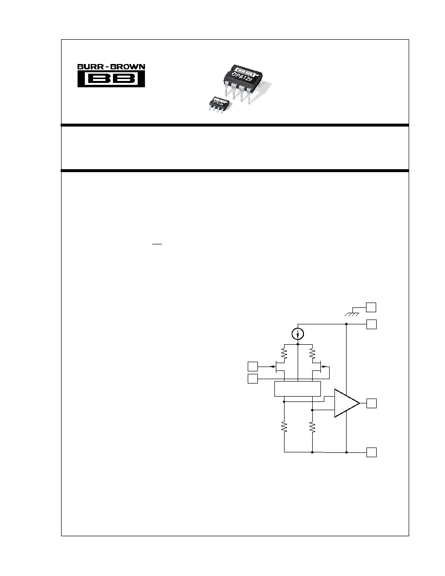
DESCRIPTION
The OPA129 is an ultra-low bias current mono-
lithic operational amplifier offered in an 8-pin PDIP
and SO-8 package. Using advanced geometry
dielectrically-isolated FET (
Difet
Æ
) inputs, this mono-
lithic amplifier achieves a high performance level.
Difet
fabrication eliminates isolation-junction leakage
current--the main contributor to input bias current
with conventional monolithic FETs. This reduces
input bias current by a factor of 10 to 100. Very low
input bias current can be achieved without resorting to
small-geometry FETs or CMOS designs which can
suffer from much larger offset voltage, voltage noise,
drift, and poor power supply rejection.
The OPA129's special pinout eliminates leakage cur-
rent that occurs with other op amps. Pins 1 and 4 have
no internal connection, allowing circuit board guard
traces--even with the surface-mount package version.
OPA129 is available in 8-pin DIP and SO-8 packages,
specified for operation from ≠40
∞
C to +85
∞
C.
OPA129
Difet
Æ
Burr-Brown Corp.
+In
Output
6
Noise-Free
Cascode
7
5
V≠
V+
30k
30k
≠In
3
2
Simplified Circuit
8
Substrate
Æ
International Airport Industrial Park ∑ Mailing Address: PO Box 11400 ∑ Tucson, AZ 85734 ∑ Street Address: 6730 S. Tucson Blvd. ∑ Tucson, AZ 85706
Tel: (520) 746-1111 ∑ Twx: 910-952-1111 ∑ Cable: BBRCORP ∑ Telex: 066-6491 ∑ FAX: (520) 889-1510 ∑ Immediate Product Info: (800) 548-6132
©
1994 Burr-Brown Corporation
PDS-1195A
Printed in U.S.A. July, 1994
SBOS026
Æ
OPA129
2
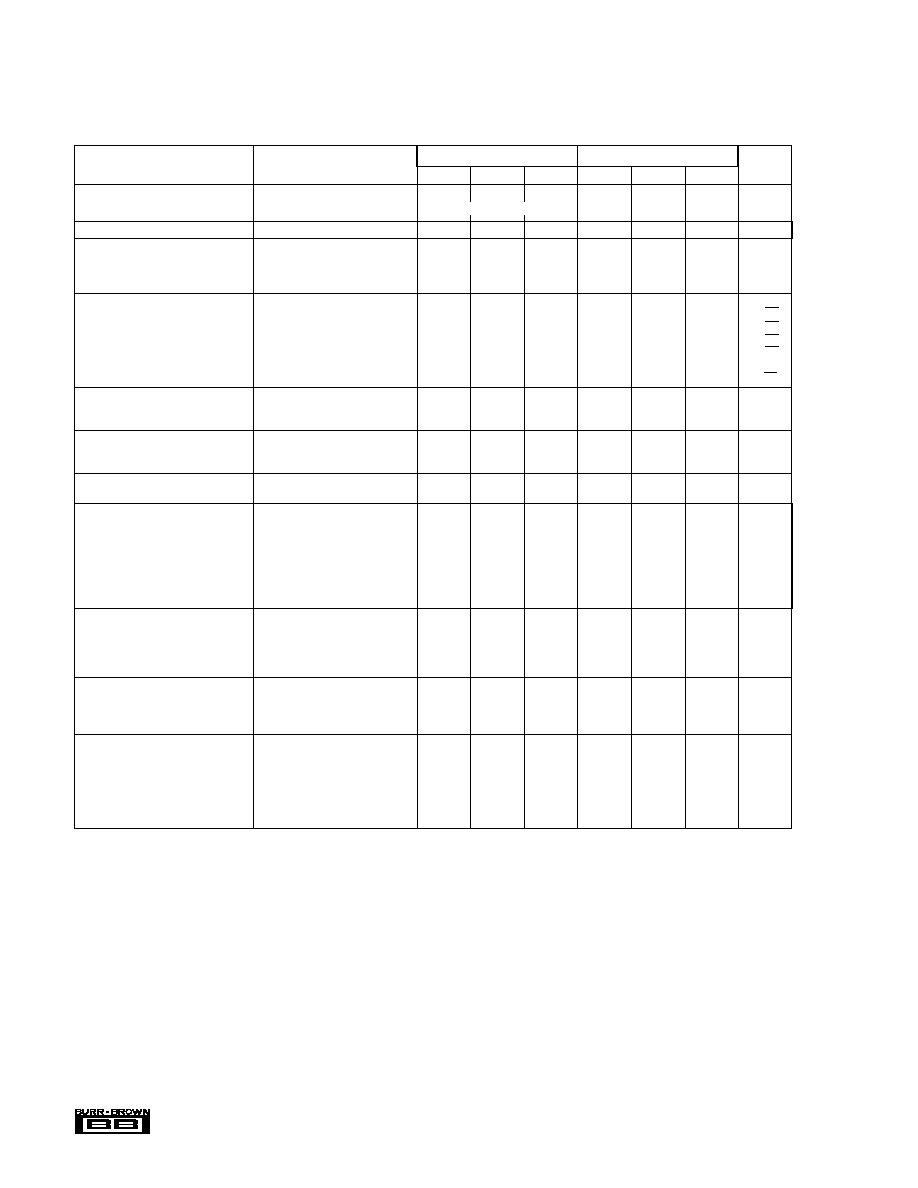
SPECIFICATIONS
ELECTRICAL
At V
S
=
±
15V and T
A
= +25
∞
C unless otherwise noted. Pin 8 connected to ground.
NOTES: (1) High-speed automated test. (2) Overload recovery is defined as the time required for the output to return from saturation to linear operation following the
removal of a 50% input overdrive.
The information provided herein is believed to be reliable; however, BURR-BROWN assumes no responsibility for inaccuracies or omissions. BURR-BROWN
assumes no responsibility for the use of this information, and all use of such information shall be entirely at the user's own risk. Prices and specifications are subject
to change without notice. No patent rights or licenses to any of the circuits described herein are implied or granted to any third party. BURR-BROWN does not
authorize or warrant any BURR-BROWN product for use in life support devices and/or systems.
OPA129PB, UB
OPA129P, U
PARAMETER
CONDITION
MIN
TYP
MAX
MIN
TYP
MAX
UNITS
INPUT BIAS CURRENT
(1)
V
CM
= 0V
±
30
±
100
*
±
250
fA
vs Temperature
Doubles every 10
∞
C
*
INPUT OFFSET CURRENT
V
CM
= 0V
±
30
*
fA
OFFSET VOLTAGE
Input Offset Voltage
V
CM
= 0V
±
0.5
±
2
±
1
±
5
mV
vs Temperature
±
3
±
10
±
5
µ
V/
∞
C
Supply Rejection
V
S
=
±
5V to
±
18V
±
3
±
100
*
*
µ
V/V
NOISE
Voltage
f = 10Hz
85
*
nV/
Hz
f = 100Hz
28
*
nV/
Hz
f = 1kHz
17
*
nV/
Hz
f = 10kHz
15
*
nV/
Hz
f
B
= 0.1Hz to 10Hz
4
*
µ
Vp-p
Current
f = 10kHz
0.1
*
fA/
Hz
INPUT IMPEDANCE
Differential
10
13
|| 1
*
|| pF
Common-Mode
10
15
|| 2
*
|| pF
VOLTAGE RANGE
Common-Mode Input Range
±
10
±
12
*
*
V
Common-Mode Rejection
V
IN
=
±
10V
80
118
*
*
dB
OPEN-LOOP GAIN, DC
Open-Loop Voltage Gain
R
L
2k
94
120
*
*
dB
FREQUENCY RESPONSE
Unity Gain, Small Signal
1
*
MHz
Full Power Response
20Vp-p, R
L
= 2k
47
*
kHz
Slew Rate
V
O
=
±
10V, R
L
= 2k
1
2.5
*
*
V/
µ
s
Settling Time:
G = ≠1, R
L
= 2k
,
10V Step
0.1%
5
*
µ
s
0.01%
10
*
µ
s
Overload Recovery, 50% Overdrive
(2)
G = ≠1
5
*
µ
s
RATED OUTPUT
Voltage Output
R
L
= 2k
±
12
±
13
*
*
V
Current Output
V
O
=
±
12V
±
6
±
10
*
*
mA
Load Capacitance Stability
Gain = +1
1000
*
pF
Short-Circuit Current
±
35
±
55
*
*
mA
POWER SUPPLY
Rated Voltage
±
15
*
V
Voltage Range, Derated Performance
±
5
±
18
*
*
V
Current, Quiescent
I
O
= 0mA
1.2
1.8
*
*
mA
TEMPERATURE
Specification
Ambient Temperature
≠40
+85
*
*
∞
C
Operating
Ambient Temperature
≠40
+125
*
*
∞
C
Storage
≠40
+125
*
*
∞
C
Thermal Resistance
JA
, Junction-to-Ambient
PDIP--"P"
90
*
∞
C/W
SOIC--"U"
100
*
∞
C/W
Æ
OPA129
3
100
1
1M
10M
1k
10k
100k
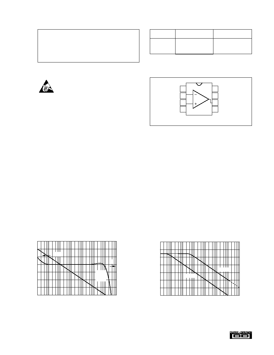
10
POWER SUPPLY REJECTION vs FREQUENCY
Frequency (Hz)
Power Supply Rejection (dB)
140
120
100
80
60
40
20
0
+PSRR
≠PSRR
OPEN-LOOP FREQUENCY RESPONSE
Frequency (Hz)
Voltage Gain (dB)
140
120
100
80
60
40
20
0
100
1
1M
10M
45
90
135
180
Pulse Shift (degrees)
Gain
1k
10k
100k
10
Phase
Margin
90∞
Power Supply Voltage ......................................................................
±
18V
Differential Input Voltage ............................................................ V≠ to V+
Input Voltage Range .................................................................... V≠ to V+
Storage Temperature Range ......................................... ≠40
∞
C to +125
∞
C
Operating Temperature Range ..................................... ≠40
∞
C to +125
∞
C
Lead Temperature (soldering, 10s; SOIC 3s) ............................... +300
∞
C
Output Short Circuit Duration
(1) ..................................................................
Continuous
Junction Temperature (T
J
) ............................................................. +150
∞
C
ABSOLUTE MAXIMUM RATINGS
NOTE: (1) Short circuit may be to power supply common at +25
∞
C ambient.
PACKAGE INFORMATION
PACKAGE DRAWING
MODEL
PACKAGE
NUMBER
(1)
OPA129P
8-pin Plastic DIP
006
OPA129PB
8-pin Plastic DIP
006
OPA129U
8-pin SOIC
182
OPA129UB
8-pin SOIC
182
NOTE: (1) For detailed drawing and dimension table, please see end of data
sheet, or Appendix D of Burr-Brown IC Data Book.
CONNECTION DIAGRAM
ELECTROSTATIC
DISCHARGE SENSITIVITY
Any integrated circuit can be damaged by ESD. Burr-Brown
recommends that all integrated circuits be handled with
appropriate precautions. Failure to observe proper handling
and installation procedures can cause damage.
ESD damage can range from subtle performance degrada-
tion to complete device failure. Precision integrated circuits
may be more susceptible to damage because very small
parametric changes could cause the device not to meet
published specifications.
Top View
DIP/SOIC
TYPICAL PERFORMANCE CURVES
T
A
= +25
∞
C, +15VDC, unless otherwise noted.
1
2
3
4
8
7
6
5
Substrate
V+
Output
V≠
NC
≠In
+In
NC
OPA
NC: No internal connection.
Æ
OPA129
4
0
Frequency (Hz)
FULL-POWER OUTPUT vs FREQUENCY
Output Voltage (Vp-p)
10k
100k
1k
1M
30
20
10
10
Frequency (Hz)
INPUT VOLTAGE NOISE SPECTRAL DENSITY
Voltage Density (nV/
Hz)
1
10
100
1k
10k
100k
1k
100
10
1
0.1
0.01
15
≠10
≠5
5
10
15
Common-Mode Voltage (V)
BIAS AND OFFSET CURRENT
vs INPUT COMMON-MODE VOLTAGE
Normalized Bias and Offset Current
0
BIAS AND OFFSET CURRENT vs TEMPERATURE
Ambient Temperature (∞C)
Bias and Offset Current (fA)
100pA
10pA
1pA
100
10
1
≠50
50
125
≠25
0
25
75
100
I
B
and I
OS
100
1
1M
10M
1k
10k
100k
10
COMMON-MODE REJECTION vs FREQUENCY
Frequency (Hz)
Common-Mode Rejection (dB)
140
120
100
80
60
40
20
0
COMMON-MODE REJECTION
vs INPUT COMMON-MODE VOLTAGE
Common-Mode Voltage (V)
Common-Mode Rejection (dB)
70
15
15
10
10
5
0
5
120
110
100
90
80
TYPICAL PERFORMANCE CURVES
(CONT)
T
A
= +25
∞
C, +15VDC, unless otherwise noted.
Æ
OPA129
5
OPEN-LOOP GAIN, PSR AND CMR vs TEMPERATURE
Ambient Temperature (∞C)
PSR, CMR, Voltage Gain (dB)
130
120
110
100
90
CMR
A
OL
PSR
≠75
125
≠50
75
≠25
0
25
50
100
SUPPLY CURRENT vs TEMPERATURE
Ambient Temperature (∞C)
Supply Current (mA)
2
1.5
1
0.5
0
≠75
125
≠50
75
≠25
0
25
50
100
0
Supply Voltage (±V
CC
)
GAIN BANDWIDTH AND SLEW RATE
vs SUPPLY VOLTAGE
Gain Bandwidth (MHz)
5
15
0
20
3
2
1
10
0
Slew Rate (v/µs)
6
4
2
+Slew
≠Slew
GBW
GAIN BANDWIDTH AND SLEW RATE
vs TEMPERATURE
Ambient Temperature (∞C)
Gain Bandwidth (MHz)
Slew Rate (V/µs)
4
3
2
1
4
3
2
1
0
0
≠75
125
≠50
75
≠25
0
25
50
100
LARGE SIGNAL TRANSIENT RESPONSE
Time (µs)
Output Voltage (V)
10
0
≠10
0
50
25
TYPICAL PERFORMANCE CURVES
(CONT)
T
A
= +25
∞
C, +15VDC, unless otherwise noted.
SMALL SIGNAL TRANSIENT RESPONSE
Time (µs)
Output Voltage (mV)
80
40
0
≠40
0
10
2
4
6
8
≠80
Æ
OPA129
6
0
Supply Voltage (±V
CC
)
COMMON-MODE INPUT RANGE vs SUPPLY VOLTAGE
Common-Mode Voltage (+V)
5
10
0
20
15
10
5
15
BIAS CURRENT vs ADDITIONAL POWER DISSIPATION
Additional Power Dissipation (mW)
Bias Current (fA)
100pA
10pA
1pA
100
10
1
0
200
350
50
100
150
250
300
TYPICAL PERFORMANCE CURVES
(CONT)
T
A
= +25
∞
C, +15VDC, unless otherwise noted.
APPLICATIONS INFORMATION
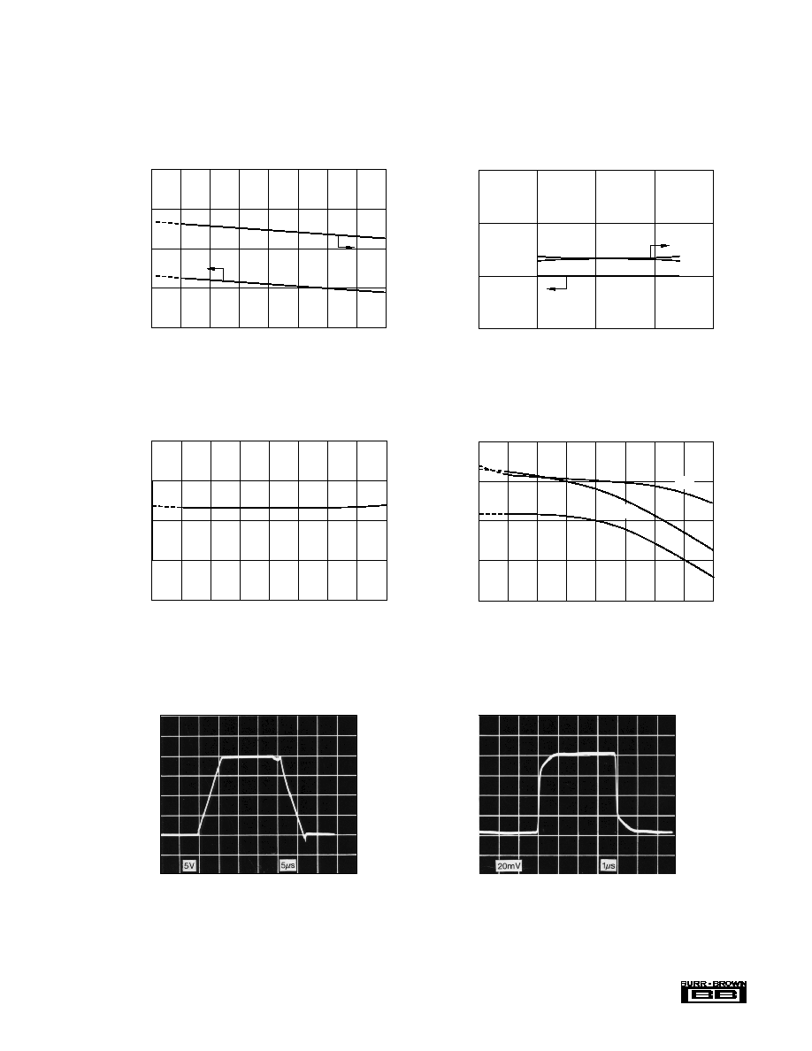
NON-STANDARD PINOUT
The OPA129 uses a non-standard pinout to achieve lowest
possible input bias current. The negative power supply is
connected to pin 5--see Figure 1. This is done to reduce the
leakage current from the V- supply (pin 4 on conventional
op amps) to the op amp input terminals. With this new
pinout, sensitive inputs are separated from both power
supply pins.
FIGURE 1. Offset Adjust Circuit.
OFFSET VOLTAGE TRIM
The OPA129 has no conventional offset trim connections.
Pin 1, next to the critical inverting input, has no internal
connection. This eliminates a source of leakage current and
allows guarding of the input terminals. Pin 1 and pin 4, next
to the two input pins, have no internal connection. This
allows an optimized circuit board layout with guarding--see
"circuit board layout."
Due to its laser-trimmed input stage, most applications do
not require external offset voltage trimming. If trimming is
required, the circuit shown in Figure 1 can be used. Power
supply voltages are divided down, filtered and applied to the
non-inverting input. The circuit shown is sensitive to varia-
tion in the supply voltages. Regulation can be added, if
needed.
GUARDING AND SHIELDING
Ultra-low input bias current op amps require precautions to
achieve best performance. Leakage current on the surface of
circuit board can exceed the input bias current of the ampli-
fier. For example, a circuit board resistance of 10
12
from
a power supply pin to an input pin produces a current of
15pA--more than one-hundred times the input bias current
of the op amp.
To minimize surface leakage, a guard trace should com-
pletely surround the input terminals and other circuitry
connecting to the inputs of the op amp. The DIP package
should have a guard trace on both sides of the circuit board.
The guard ring should be driven by a circuit node equal in
potential to the op amp inputs--see Figure 2. The substrate,
pin 8, should also be connected to the circuit board guard to
assure that the amplifier is fully surrounded by the guard
potential. This minimizes leakage current and noise pick-up.
Careful shielding is required to reduce noise pickup. Shield-
ing near feedback components may also help reduce noise
pick-up.
Triboelectric effects (friction-generated charge) can be a
troublesome source of errors. Vibration of the circuit board,
input connectors and input cables can cause noise and drift.
Make the assembly as rigid as possible. Attach cables to
avoid motion and vibration. Special low noise or low leak-
age cables may help reduce noise and leakage current. Keep
all input connections as short possible. Surface-mount com-
ponents may reduce circuit board size and allow a more rigid
assembly.
OPA129
V
OUT
V
IN
R
F
R
IN
2
3
6
7
5
V+
V≠
0.1µF
220
470k
470k
V≠
V+
Æ
OPA129
7
CIRCUIT BOARD LAYOUT
The OPA129 uses a new pinout for ultra low input bias
current. Pin 1 and pin 4 have no internal connection. This
allows ample circuit board space for a guard ring surround-
ing the op amp input pins--even with the tiny SO-8 surface-
mount package. Figure 3 shows suggested circuit board
layouts. The guard ring should be connected to pin 8 (sub-
strate) as shown. It should be driven by a circuit node equal
in potential to the input terminals of the op amp--see Figure
2 for common circuit configurations.
TESTING
Accurately testing the OPA129 is extremely difficult due to
its high performance. Ordinary test equipment may not be
able to resolve the amplifier's extremely low bias current.
Inaccurate bias current measurements can be due to:
1. Test socket leakage,
2. Unclean package,
3. Humidity or dew point condensations,
4. Circuit contamination from fingerprints or anti-static
treatment chemicals,
5. Test ambient temperature,
6. Load power dissipation,
7. Mechanical stress,
8. Electrostatic and electromagnetic interference.
1
8
5
4
1
8
5
4
(A) DIP package
(B) SOIC package
V≠
V
0
V+
V≠
V
0
V+
Connect to proper circuit
node, depending on circuit
configuration (see Figure 2).
Connect to proper circuit
node, depending on circuit
configuration (see Figure 2).
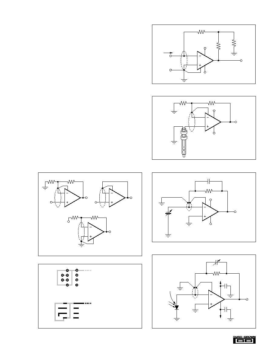
FIGURE 7. Sensitive Photodiode Amplifier.
2
3
6
8
OPA129
Output
Pin photodiode
HP 5082-4204
5
7
+15V
≠15V
0.1µF
5 x 10
9
V/W
0.1µF
10
10
~1pF to prevent gain peaking
Guard
Circuit must be well shielded.
Out
In
2
3
6
8
(C) Inverting
Out
In
2
3
6
8
(A) Non-Inverting
Out
In
2
3
6
8
(B) Buffer
Guard top and bottom of board.
FIGURE 2. Connection of Input Guard.
FIGURE 3. Suggested Board Layout for Input Guard.
FIGURE 5. High Impedance (10
15
) Amplifier.
FIGURE 6. Piezoelectric Transducer Charge Amplifier.
1VDC
Output
2
3
6
8
Guard
500
9.5k
OPA129
pH Probe
R
S
500M
50mV Out
7
5
V≠
V+
FIGURE 4. Current-to-Voltage Converter.
2
3
6
7
5
8
OPA129
1000M
R
F
Output
V
O
= ≠I
IN
∑ R
F
V
O
= ≠1V/nA
18k
2k
Current
Input
I
IN
V≠
V+
V
OUT
2
3
6
8
C
F
OPA129
Low frequency cutoff =
1/(2
R
F
C
F
) = 0.16Hz
10pF
10
11
Output
V
OUT
= ≠
Q/C
F
Q
R
F
7
5
V≠
V+

PACKAGING INFORMATION
ORDERABLE DEVICE
STATUS(1)
PACKAGE TYPE
PACKAGE DRAWING
PINS
PACKAGE QTY
OPA129P
OBSOLETE
PDIP
P
8
OPA129PB
OBSOLETE
PDIP
P
8
OPA129U
ACTIVE
SOIC
D
8
100
OPA129UB
ACTIVE
SOIC
D
8
100
OPA129UB/2K5
ACTIVE
SOIC
D
8
2500
(1) The marketing status values are defined as follows:
ACTIVE: Product device recommended for new designs.
LIFEBUY: TI has announced that the device will be discontinued, and a lifetime-buy period is in effect.
NRND: Not recommended for new designs. Device is in production to support existing customers, but TI does not recommend using this part in
a new design.
PREVIEW: Device has been announced but is not in production. Samples may or may not be available.
OBSOLETE: TI has discontinued the production of the device.
PACKAGE OPTION ADDENDUM
www.ti.com
3-Oct-2003

IMPORTANT NOTICE
Texas Instruments Incorporated and its subsidiaries (TI) reserve the right to make corrections, modifications,
enhancements, improvements, and other changes to its products and services at any time and to discontinue
any product or service without notice. Customers should obtain the latest relevant information before placing
orders and should verify that such information is current and complete. All products are sold subject to TI's terms
and conditions of sale supplied at the time of order acknowledgment.
TI warrants performance of its hardware products to the specifications applicable at the time of sale in
accordance with TI's standard warranty. Testing and other quality control techniques are used to the extent TI
deems necessary to support this warranty. Except where mandated by government requirements, testing of all
parameters of each product is not necessarily performed.
TI assumes no liability for applications assistance or customer product design. Customers are responsible for
their products and applications using TI components. To minimize the risks associated with customer products
and applications, customers should provide adequate design and operating safeguards.
TI does not warrant or represent that any license, either express or implied, is granted under any TI patent right,
copyright, mask work right, or other TI intellectual property right relating to any combination, machine, or process
in which TI products or services are used. Information published by TI regarding third-party products or services
does not constitute a license from TI to use such products or services or a warranty or endorsement thereof.
Use of such information may require a license from a third party under the patents or other intellectual property
of the third party, or a license from TI under the patents or other intellectual property of TI.
Reproduction of information in TI data books or data sheets is permissible only if reproduction is without
alteration and is accompanied by all associated warranties, conditions, limitations, and notices. Reproduction
of this information with alteration is an unfair and deceptive business practice. TI is not responsible or liable for
such altered documentation.
Resale of TI products or services with statements different from or beyond the parameters stated by TI for that
product or service voids all express and any implied warranties for the associated TI product or service and
is an unfair and deceptive business practice. TI is not responsible or liable for any such statements.
Following are URLs where you can obtain information on other Texas Instruments products and application
solutions:
Products
Applications
Amplifiers
amplifier.ti.com
Audio
www.ti.com/audio
Data Converters
dataconverter.ti.com
Automotive
www.ti.com/automotive
DSP
dsp.ti.com
Broadband
www.ti.com/broadband
Interface
interface.ti.com
Digital Control
www.ti.com/digitalcontrol
Logic
logic.ti.com
Military
www.ti.com/military
Power Mgmt
power.ti.com
Optical Networking
www.ti.com/opticalnetwork
Microcontrollers
microcontroller.ti.com
Security
www.ti.com/security
Telephony
www.ti.com/telephony
Video & Imaging
www.ti.com/video
Wireless
www.ti.com/wireless
Mailing Address:
Texas Instruments
Post Office Box 655303 Dallas, Texas 75265
Copyright
2003, Texas Instruments Incorporated