Document Outline
- FEATURES
- DESCRIPTION
- ABSOLUTE MAXIMUM RATINGS
- PACKAGE/ORDERING INFORMATION
- ELECTRICAL CHARACTERISTICS
- TYPICAL CHARACTERISTICS
- APPLICATIONS INFORMATION
- OFFSET VOLTAGE TRIM
- INPUT BIAS CURRENT
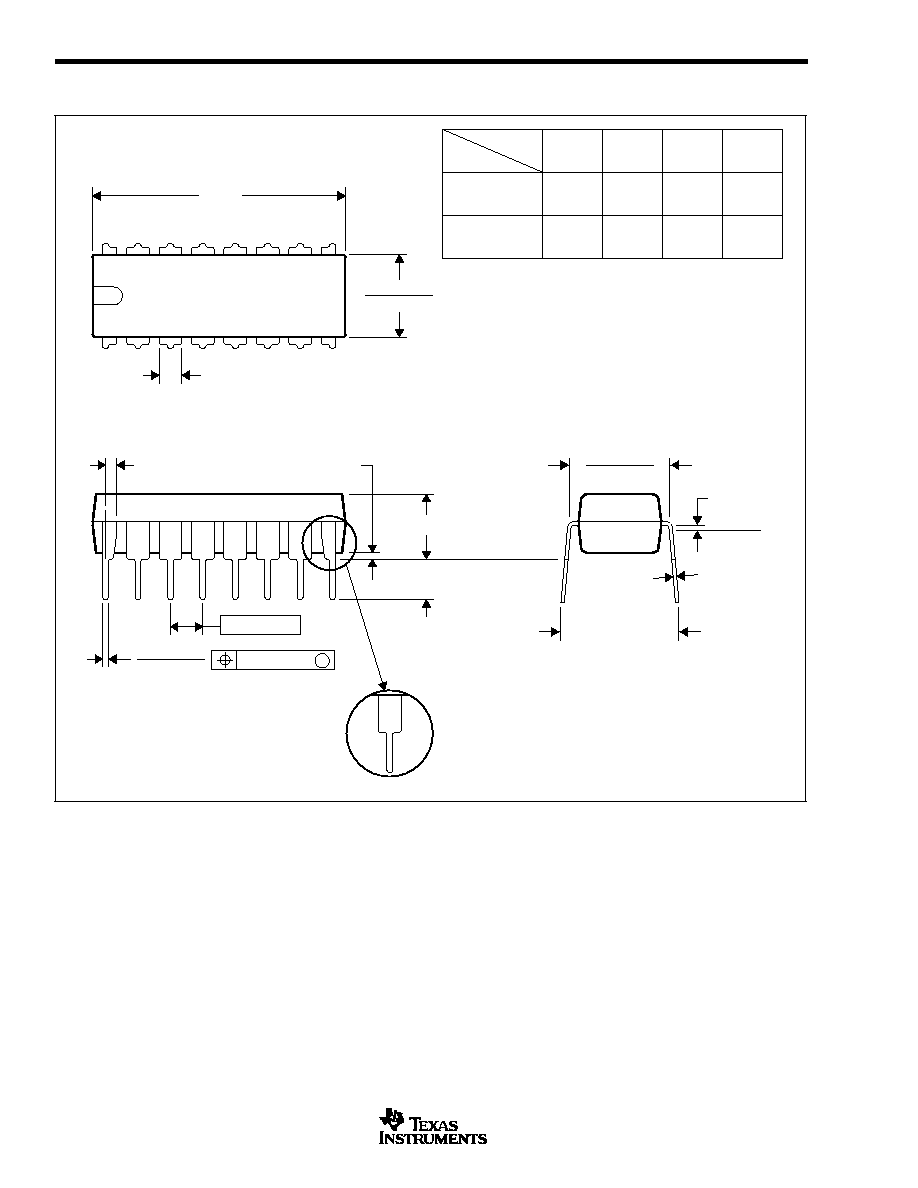
- PACKAGE DRAWINGS
- D (R-PDSO-G**) PLASTIC SMALL-OUTLINE PACKAGE
- DW (R-PDSO-G**) PLASTIC SMALL-OUTLINE PACKAGE
- N (R-PDIP-T**) PLASTIC DUAL-IN-LINE PACKAGE
FEATURES
q
FET INPUT: I
B
= 50pA max
q
LOW OFFSET VOLTAGE: 750
µ
V max
q
WIDE SUPPLY RANGE:
±
4.5V to
±
18V
q
SLEW RATE: 10V/
µ
s
q
WIDE BANDWIDTH: 4MHz
q
EXCELLENT CAPACITIVE LOAD DRIVE
q
SINGLE, DUAL, QUAD VERSIONS
General-Purpose
FET-INPUT OPERATIONAL AMPLIFIERS
DESCRIPTION
The OPA131 series of FET-input op amps provides high
performance at low cost. Single, dual, and quad versions in
industry-standard pinouts allow cost-effective design op-
tions.
The OPA131 series offers excellent general-purpose perfor-
mance, including low offset voltage, drift, and good dynamic
characteristics.
Single, dual, and quad versions are available in DIP and SO
packages. Performance grades include commercial and in-
dustrial temperature ranges.
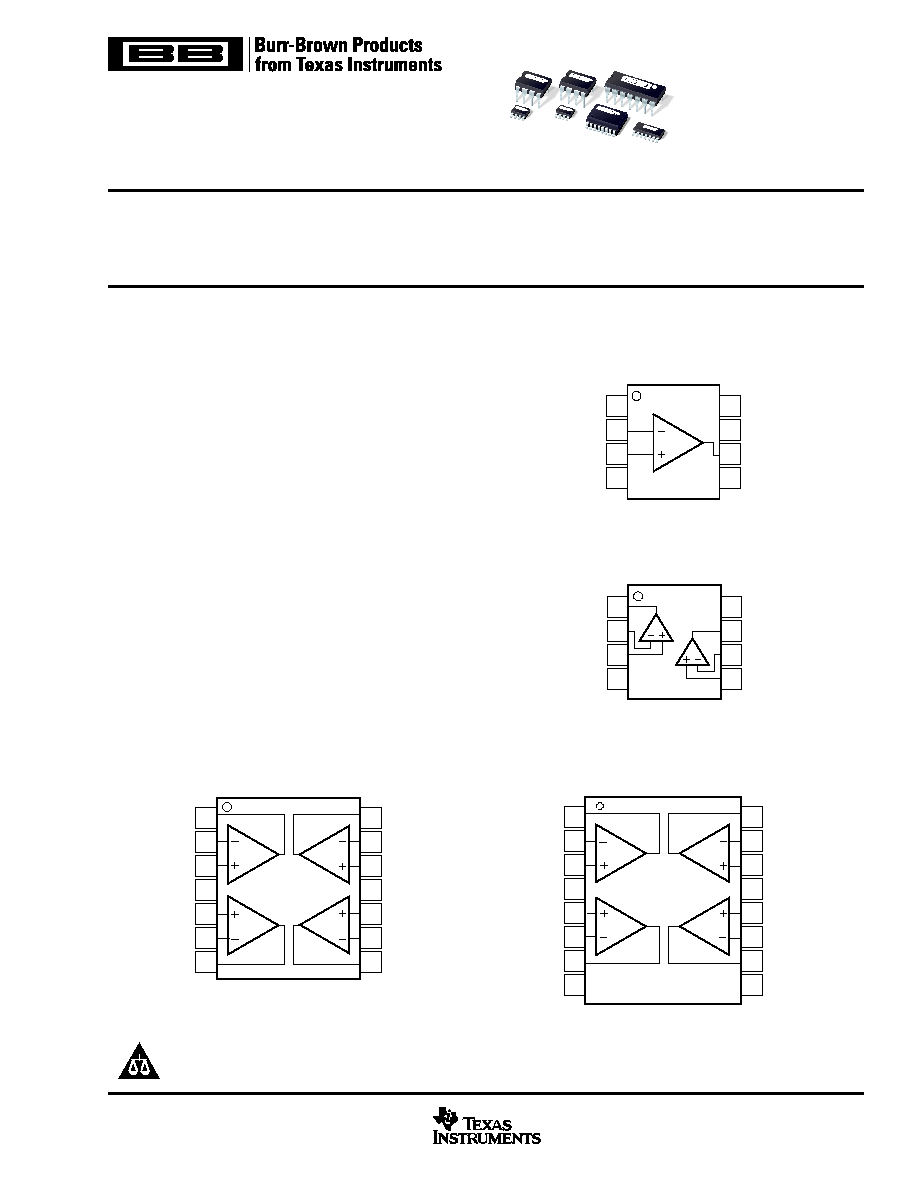
1
2
3
4
5
6
7
14
13
12
11
10
9
8
Out D
≠In D
+In D
V≠
+In C
≠In C
Out C
Out A
≠In A
+In A
V+
+In B
≠In B
Out B
OPA4131
DIP-14, SO-14
A
D
B
C
1
2
3
4
8
7
6
5
NC
V+
Output
Offset Trim
Offset Trim
≠In
+In
V≠
OPA131
DIP-8, SO-8
1
2
3
4
5
6
7
8
16
15
14
13
12
11
10
9
Out D
≠In D
+In D
V≠
+In C
≠In C
Out C
NC
Out A
≠In A
+In A
V+
+In B
≠In B
Out B
NC
OPA4131
SOL-16
A
D
B
C
OPA131
OPA2
131
OPA1
31
OPA2
131
OPA41
31
OPA
413
1
OPA4
131
1
2
3
4
8
7
6
5
V+
Out B
≠In B
+In B
Out A
≠In A
+In A
V≠
OPA2131
DIP-8, SO-8
A
B
OPA131
OPA2131
OPA4131
SBOS040A ≠ NOVEMBER 1994 ≠ REVISED DECEMBER 2002
www.ti.com
PRODUCTION DATA information is current as of publication date.
Products conform to specifications per the terms of Texas Instruments
standard warranty. Production processing does not necessarily include
testing of all parameters.
Copyright © 1994, Texas Instruments Incorporated
Please be aware that an important notice concerning availability, standard warranty, and use in critical applications of
Texas Instruments semiconductor products and disclaimers thereto appears at the end of this data sheet.
NC = No Connection
OPA131, 2131, 4131
2
SBOS040A
www.ti.com
SPECIFIED
PACKAGE
TEMPERATURE
PACKAGE
ORDERING
TRANSPORT
PRODUCT
PACKAGE-LEAD
DESIGNATOR
(1)
RANGE
MARKING
NUMBER
MEDIA, QUANTITY
Single
OPA131
SO-8
D
≠40
∞
C to +85
∞
C
OPA131UJ
OPA131UJ
Rails, 100
"
"
"
"
"
OPA131UJ/2K5
Tape and Reel, 2500
OPA131
SO-8
D
≠40
∞
C to +85
∞
C
OPA131UA
OPA131UA
Rails, 100
"
"
"
"
"
OPA131UA/2K5
Tape and Reel, 2500
OPA131
SO-8
D
≠40
∞
C to +85
∞
C
OPA131U
OPA131U
Rails, 100
"
"
"
"
"
OPA131U/2K5
Tape and Reel, 2500
Dual
OPA2131
SO-8
D
≠40
∞
C to +85
∞
C
OPA2131UJ
OPA2131UJ
Rails, 100
"
"
"
"
"
OPA2131UJ/2K5
Tape and Reel, 2500
OPA2131
SO-8
D
≠40
∞
C to +85
∞
C
OPA2131UA
OPA2131UA
Rails, 100
"
"
"
"
"
OPA2131UA/2K5
Tape and Reel, 2500
Quad
OPA4131
DIP-14
N
≠40
∞
C to +85
∞
C
OPA4131PJ
OPA4131PJ
Rails, 25
"
"
"
"
OPA4131PA
OPA4131PA
Rails, 25
OPA4131
SOL-16
DW
≠40
∞
C to +85
∞
C
OPA4131UA
OPA4131UA
Rails, 48
"
"
"
"
"
OPA4131UA/1K
Tape and Reel, 1000
OPA4131
SOL-14
D
≠40
∞
C to +85
∞
C
OPA4131NJ
OPA4131NJ
Rails, 58
"
"
"
"
OPA4131NA
OPA4131NA
Rails, 58
ABSOLUTE MAXIMUM RATINGS
(1)
Supply Voltage, V+ to V≠ .................................................................... 36V
Input Voltage .................................................. (V≠) ≠ 0.7V to (V+) + 0.7V
Output Short-Circuit
(2)
.............................................................. Continuous
Operating Temperature .................................................. ≠55
∞
C to +125
∞
C
Storage Temperature ..................................................... ≠55
∞
C to +125
∞
C
Junction Temperature ...................................................................... 150
∞
C
Lead Temperature (soldering, 10s) ................................................. 300
∞
C
NOTES: (1) Stresses above these ratings may cause permanent damage.
Exposure to absolute maximum conditions for extended periods may degrade
device reliability. (2) Short-circuit to ground, one amplifier per package.
ELECTROSTATIC
DISCHARGE SENSITIVITY
This integrated circuit can be damaged by ESD. Texas Instru-
ments recommends that all integrated circuits be handled with
appropriate precautions. Failure to observe proper handling
and installation procedures can cause damage.
ESD damage can range from subtle performance degradation
to complete device failure. Precision integrated circuits may be
more susceptible to damage because very small parametric
changes could cause the device not to meet its published
specifications.
PACKAGE/ORDERING INFORMATION
NOTE: (1) For the most current specifications and package information, refer to our web site at www.ti.com.
OPA131, 2131, 4131
3
SBOS040A
www.ti.com
ELECTRICAL CHARACTERISTICS
At T
A
= +25
∞
C, V
S
=
±
15V, and R
L
= 2k
,
unless otherwise noted.
OPA131UA
OPA2131UA
OPA4131PA, UA, NA
OPA131UJ
OPA2131UJ
OPA4131PJ, NJ
PARAMETER
CONDITION
MIN
TYP
MAX
MIN
TYP
MAX
UNITS
OFFSET VOLTAGE
Input Offset Voltage
±
0.2
±
1
±
1.5
mV
OPA131U model only
±
0.2
0.75
mV
vs Temperature
(1)
Operating Temperature Range
±
2
±
10
µ
V/
∞
C
vs Power Supply
V
S
=
±
4.5V to
±
18V
50
200
µ
V/V
OPA131U model only
50
100
µ
V/V
INPUT BIAS CURRENT
(2)
Input Bias Current
V
CM
= 0V
+5
±
50
pA
vs Temperature
See Typical Characteristic
Input Offset Current
V
CM
= 0V
±
1
±
50
pA
NOISE
Input Voltage Noise
Noise Density, f = 10Hz
21
nV/
Hz
f = 100Hz
16
nV/
Hz
f = 1kHz
15
nV/
Hz
f = 10kHz
15
nV/
Hz
Current Noise Density, f = 1kHz
3
fA/
Hz
INPUT VOLTAGE RANGE
Common-Mode Voltage Range
(V≠) + 3
(V+) ≠ 1
V
Common-Mode Rejection
V
CM
= ≠12V to +14V
70
80
dB
OPA131U model only
80
86
dB
INPUT IMPEDANCE
Differential
10
10
|| 1
|| pF
Common-Mode
V
CM
= 0V
10
12
|| 3
|| pF
OPEN-LOOP GAIN
Open-Loop Voltage Gain
V
O
= ≠12V to +12V
94
110
dB
OPA131U model only
100
110
dB
FREQUENCY RESPONSE
Gain-Bandwidth Product
4
MHz
Slew Rate
10
V/
µ
s
Settling Time 0.1%
G = ≠1, 10V Step, C
L
= 100pF
1.5
µ
s
0.01%
G = ≠1, 10V Step, C
L
= 100pF
2
µ
s
Total Harmonic Distortion + Noise
1kHz, G = 1, V
O
= 3.5Vrms
0.0008
%
OUTPUT
Voltage Output, Positive
(V+) ≠ 3 (V+) ≠ 2.5
V
Negative
(V≠) + 3 (V≠) + 2.5
V
Short-Circuit Current
±
25
mA
POWER SUPPLY
Specified Operating Voltage
±
15
V
Operating Voltage Range
±
4.5
±
18
V
Quiescent Current (per amplifier)
I
O
= 0
±
1.5
±
1.75
±
2
mA
TEMPERATURE RANGE
Operating Range
≠55
+125
≠55
+125
∞
C
Storage
≠55
+125
∞
C
Thermal Resistance,
JA
DIP-8
100
∞
C/W
SO-8
150
∞
C/W
DIP-14
80
∞
C/W
SO-14, SOL-16
110
∞
C/W
Specifications same as OPA131UA.
NOTES: (1) Ensured by wafer test. (2) High-speed test at T
J
= 25
∞
C.
OPA131, 2131, 4131
4
SBOS040A
www.ti.com
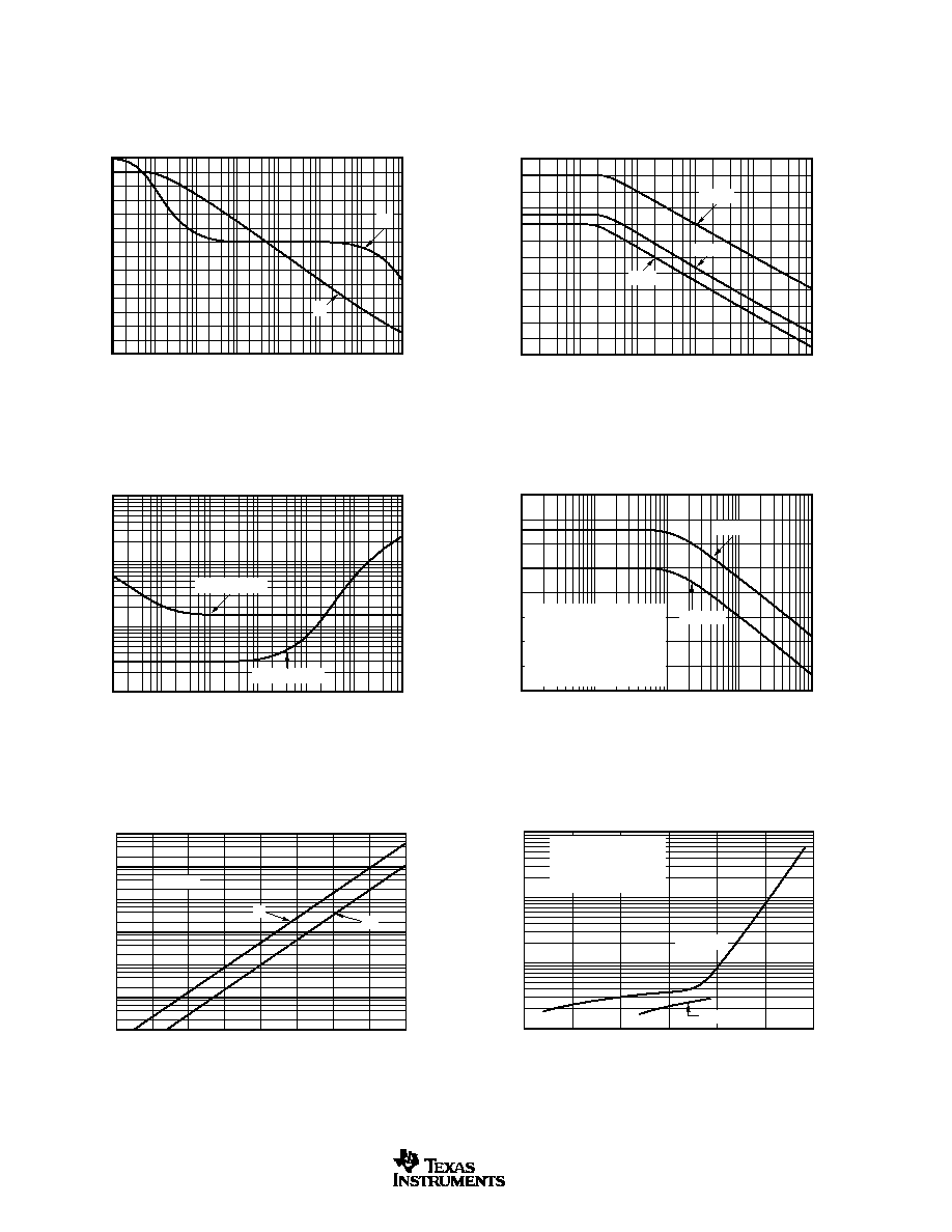
TYPICAL CHARACTERISTICS
At T
A
= +25
∞
C, V
S
=
±
15V, and R
L
= 2k
,
unless otherwise noted.
POWER SUPPLY AND COMMON-MODE REJECTION
vs FREQUENCY
Frequency (Hz)
Power Supply Rejection (dB)
120
100
80
60
40
20
0
Common-Mode Rejection (dB)
120
100
80
60
40
20
0
10
100
1k
10k
100k
1M
CMR
+PSR
≠PSR
CHANNEL SEPARATION vs FREQUENCY
Frequency (Hz)
Channel Separation (dB)
160
140
120
100
80
10
100
1k
10k
100k
Dual and quad devices.
G = 1, all channels.
Quad measured channel
A to D or B to C--other
combinations yield improved
rejection.
R
L
=
R
L
= 2k
OPEN-LOOP GAIN/PHASE vs FREQUENCY
1
120
100
80
60
40
20
0
≠20
Voltage Gain (dB)
0
≠45
≠90
≠135
≠180
Phase Shift (
∞
)
Frequency (Hz)
10
100
1k
10k
100k
1M
10M
G
INPUT BIAS AND INPUT OFFSET CURRENT
vs TEMPERATURE
Ambient Temperature (
∞
C)
Input Bias and Input Offset Current (pA)
10k
1k
100
10
1
0.1
0.01
≠75
≠50
≠25
0
25
50
75
100
125
I
B
I
OS
V
CM
= 0V
INPUT BIAS CURRENT
vs INPUT COMMON-MODE VOLTAGE
Common-Mode Voltage (V)
Input Bias Current (pA)
1k
100
10
1
≠15
≠10
≠5
0
5
10
15
Input bias current is a
function of the voltage
between the V≠ supply
and the inputs.
V
S
=
±
15V
V
S
=
±
5V
INPUT VOLTAGE AND CURRENT NOISE
SPECTRAL DENSITY vs FREQUENCY
1
1k
100
10
Voltage Noise (nV/
Hz)
Frequency (Hz)
10
100
1k
10k
100k
1M
1
1k
100
10
Current Noise (fA/
Hz)
1
Voltage Noise
Current Noise

OPA131, 2131, 4131
5
SBOS040A
www.ti.com
TYPICAL CHARACTERISTICS
(Cont.)
At T
A
= +25
∞
C, V
S
=
±
15V, and R
L
= 2k
,
unless otherwise noted.
QUIESCENT CURRENT AND SHORT-CIRCUIT CURRENT
vs TEMPERATURE
Temperature (
∞
C)
Quiescent Current (mA)
1.8
1.6
1.4
1.2
1
Short-Circuit Current (mA)
40
30
20
10
0
≠75
≠50
≠25
0
25
50
75
100
125
I
SC+
I
SC≠
I
Q
V
S
=
±
5V
I
Q
V
S
=
±
15V
OFFSET VOLTAGE DRIFT
PRODUCTION DISTRIBUTION
Units (%)
Offset Voltage Drift (
µ
V/
∞
C)
≠7 ≠6 ≠5 ≠4 ≠3 ≠2 ≠1
0
1
2
3
4
5
6
7
35
30
25
20
15
10
5
0
Typical production distribution
of packaged units. Single,
dual and quad units included.
OPEN-LOOP GAIN vs TEMPERATURE
Ambient Temperature (
∞
C)
Voltage Gain (dB)
120
115
110
105
100
≠75
≠50
≠25
0
25
50
75
100
125
OFFSET VOLTAGE
PRODUCTION DISTRIBUTION
Units (%)
Offset Voltage (
µ
V)
≠
1400
≠
1200
≠
1000
≠
800
≠
600
≠
400
≠
200
0
200
400
600
800
1000
1200
1400
20
15
10
5
0
Typical production distribution
of packaged units. Single,
dual and quad units included.
TOTAL HARMONIC DISTORTION + NOISE
vs FREQUENCY
Frequency (Hz)
THD + Noise (%)
1
0.1
0.01
0.001
0.0001
10
100
1k
10k
100k
G = 1V/V
G = 100V/V
V
O
= 3.5Vrms
G = 10V/V
Bandwidth-
Limited
MAXIMUM OUTPUT VOLTAGE
vs FREQUENCY
1M
Frequency (Hz)
10k
100k
V
S
=
±
5V
Maximum output voltage
without slew-rate induced
distortion.
10M
30
20
10
0
Output Voltage (Vp-p)
V
S
=
±
15V
OPA131, 2131, 4131
6
SBOS040A
www.ti.com
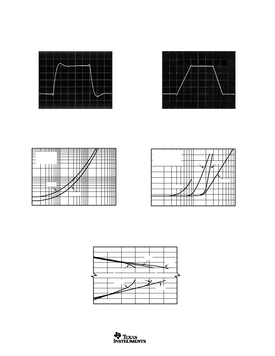
SMALL-SIGNAL STEP RESPONSE
G =1, C
L
= 300pF
200ns/div
50mV/div
TYPICAL CHARACTERISTICS
(Cont.)
At T
CASE
= +25
∞
C, V
S
=
±
15V, and R
L
= 2k
, unless otherwise noted.
LARGE-SIGNAL STEP RESPONSE
G = 1, C
L
= 300pF
5V/div
1
µ
s/div
SMALL-SIGNAL OVERSHOOT
vs LOAD CAPACITANCE
Load Capacitance
Overshoot (%)
50
40
30
20
10
0
100pF
1nF
10nF
R
L
= 2k
Higher R
L
value
generally reduces
overshoot.
G = +2
G = ≠1
G =
±
10
G = 1
OUTPUT VOLTAGE SWING vs OUTPUT CURRENT
15
14
13
12
11
10
≠10
≠11
≠12
≠13
≠14
≠15
0
5
10
15
20
25
30
Output Current
(mA)
Output Voltage Swing (V)
≠55
∞
C
≠55
∞
C
25
∞
C
125
∞
C
125
∞
C
25
∞
C
V
IN
= ≠15V
V
IN
= 15V
SETTLING TIME vs CLOSED-LOOP GAIN
Closed-Loop Gain (V/V)
Settling Time (
µ
s)
100
10
1
≠1
≠10
≠100
≠1000
V
O
= 10V Step
R
L
= 2k
C
L
= 100pF
0.1%
0.01%
OPA131, 2131, 4131
7
SBOS040A
www.ti.com
APPLICATIONS INFORMATION
The OPA131 series op amps are unity-gain stable and
suitable for a wide range of general-purpose applications.
Power-supply pins should be bypassed with 10nF ceramic
capacitors or larger.
The OPA131 series op amps are free from unexpected
output phase-reversal common with FET op amps. Many
FET-input op amps exhibit phase-reversal of the output when
the input common-mode voltage range is exceeded. This can
occur in voltage-follower circuits, causing serious problems
in control-loop applications. All circuitry is completely inde-
pendent in dual and quad versions, assuring normal behavior
when one amplifier in a package is overdriven or short-
circuited.
OFFSET VOLTAGE TRIM
The OPA131 (single op amp version) provides offset volt-
age trim connections on pins 1 and 5. Offset voltage can be
adjusted by connecting a potentiometer as shown in Figure
1. This adjustment should be used only to null the offset of
the op amp, not system offset or offset produced by the
signal source.
V+
V≠
100k
OPA131
(Single op amp only)
Trim Range:
±
20mV typ
OPA131
6
7
5
4
3
2
1
FIGURE 1. OPA131 Offset Voltage Trim Circuit.
INPUT BIAS CURRENT
The input bias current is approximately 5pA at room tem-
perature and increases with temperature as shown in the
typical characteristic "Input Bias Current vs Temperature."
Input bias current also varies with common-mode voltage
and power supply voltage. This variation is dependent on the
voltage between the negative power supply and the com-
mon-mode input voltage. The effect is shown in the typical
curve "Input Bias Current vs Common-Mode Voltage."
OPA131, 2131, 4131
8
SBOS040A
www.ti.com
PACKAGE DRAWINGS
D (R-PDSO-G**)
PLASTIC SMALL-OUTLINE PACKAGE
8 PINS SHOWN
8
0.197
(5,00)
A MAX
A MIN
(4,80)
0.189
0.337
(8,55)
(8,75)
0.344
14
0.386
(9,80)
(10,00)
0.394
16
DIM
PINS **
4040047/E 09/01
0.069 (1,75) MAX
Seating Plane
0.004 (0,10)
0.010 (0,25)
0.010 (0,25)
0.016 (0,40)
0.044 (1,12)
0.244 (6,20)
0.228 (5,80)
0.020 (0,51)
0.014 (0,35)
1
4
8
5
0.150 (3,81)
0.157 (4,00)
0.008 (0,20) NOM
0
∞
≠ 8
∞
Gage Plane
A
0.004 (0,10)
0.010 (0,25)
0.050 (1,27)
NOTES: A. All linear dimensions are in inches (millimeters).
B. This drawing is subject to change without notice.
C. Body dimensions do not include mold flash or protrusion, not to exceed 0.006 (0,15).
D. Falls within JEDEC MS-012
OPA131, 2131, 4131
9
SBOS040A
www.ti.com
PACKAGE DRAWINGS (Cont.)
DW (R-PDSO-G**)
PLASTIC SMALL-OUTLINE PACKAGE
16 PINS SHOWN
4040000 / E 08/01
Seating Plane
0.400 (10,15)
0.419 (10,65)
0.104 (2,65) MAX
1
0.012 (0,30)
0.004 (0,10)
A
8
16
0.020 (0,51)
0.014 (0,35)
0.291 (7,39)
0.299 (7,59)
9
0.010 (0,25)
0.050 (1,27)
0.016 (0,40)
(15,24)
(15,49)
PINS **
0.010 (0,25) NOM
A MAX
DIM
A MIN
Gage Plane
20
0.500
(12,70)
(12,95)
0.510
(10,16)
(10,41)
0.400
0.410
16
0.600
24
0.610
(17,78)
28
0.700
(18,03)
0.710
0.004 (0,10)
M
0.010 (0,25)
0.050 (1,27)
0
∞
≠ 8
∞
(11,51)
(11,73)
0.453
0.462
18
NOTES: A. All linear dimensions are in inches (millimeters).
B. This drawing is subject to change without notice.
C. Body dimensions do not include mold flash or protrusion not to exceed 0.006 (0,15).
D. Falls within JEDEC MS-013
OPA131, 2131, 4131
10
SBOS040A
www.ti.com
PACKAGE DRAWINGS (Cont.)
N (R-PDIP-T**)
PLASTIC DUAL-IN-LINE PACKAGE
0.325 (8,26)
0.300 (7,62)
0.010 (0,25) NOM
Gauge Plane
0.015 (0,38)
0.430 (10,92) MAX
20
0.975
(24,77)
0.940
(23,88)
18
0.920
0.850
14
0.775
0.745
(19,69)
(18,92)
16
0.775
(19,69)
(18,92)
0.745
A MIN
DIM
A MAX
PINS **
(23,37)
(21,59)
Seating Plane
14/18 PIN ONLY
4040049/D 02/00
9
8
0.070 (1,78) MAX
A
0.035 (0,89) MAX
0.020 (0,51) MIN
16
1
0.015 (0,38)
0.021 (0,53)
0.200 (5,08) MAX
0.125 (3,18) MIN
0.240 (6,10)
0.260 (6,60)
M
0.010 (0,25)
0.100 (2,54)
16 PINS SHOWN
NOTES: A. All linear dimensions are in inches (millimeters).
B. This drawing is subject to change without notice.
C. Falls within JEDEC MS-001 (20-pin package is shorter than MS-001).
PACKAGING INFORMATION
ORDERABLE DEVICE
STATUS(1)
PACKAGE TYPE
PACKAGE DRAWING
PINS
PACKAGE QTY
OPA131P
OBSOLETE
PDIP
P
8
OPA131PA
OBSOLETE
PDIP
P
8
OPA131PJ
OBSOLETE
PDIP
P
8
OPA131U
ACTIVE
SOIC
D
8
100
OPA131U/2K5
ACTIVE
SOIC
D
8
2500
OPA131UA
ACTIVE
SOIC
D
8
100
OPA131UA/2K5
ACTIVE
SOIC
D
8
2500
OPA131UJ
ACTIVE
SOIC
D
8
100
OPA131UJ/2K5
ACTIVE
SOIC
D
8
2500
OPA2131PA
OBSOLETE
PDIP
P
8
OPA2131PJ
OBSOLETE
PDIP
P
8
OPA2131UA
ACTIVE
SOIC
D
8
100
OPA2131UA/2K5
ACTIVE
SOIC
D
8
2500
OPA2131UJ
ACTIVE
SOIC
D
8
100
OPA2131UJ/2K5
ACTIVE
SOIC
D
8
2500
OPA4131NA
ACTIVE
SOIC
D
14
58
OPA4131NJ
ACTIVE
SOIC
D
14
58
OPA4131PA
ACTIVE
PDIP
N
14
25
OPA4131PJ
ACTIVE
PDIP
N
14
25
OPA4131UA
ACTIVE
SOIC
DW
16
48
OPA4131UA/1K
ACTIVE
SOIC
DW
16
1000
(1) The marketing status values are defined as follows:
ACTIVE: Product device recommended for new designs.
LIFEBUY: TI has announced that the device will be discontinued, and a lifetime-buy period is in effect.
NRND: Not recommended for new designs. Device is in production to support existing customers, but TI does not recommend using this part in
a new design.
PREVIEW: Device has been announced but is not in production. Samples may or may not be available.
OBSOLETE: TI has discontinued the production of the device.
PACKAGE OPTION ADDENDUM
www.ti.com
3-Oct-2003

IMPORTANT NOTICE
Texas Instruments Incorporated and its subsidiaries (TI) reserve the right to make corrections, modifications,
enhancements, improvements, and other changes to its products and services at any time and to discontinue
any product or service without notice. Customers should obtain the latest relevant information before placing
orders and should verify that such information is current and complete. All products are sold subject to TI's terms
and conditions of sale supplied at the time of order acknowledgment.
TI warrants performance of its hardware products to the specifications applicable at the time of sale in
accordance with TI's standard warranty. Testing and other quality control techniques are used to the extent TI
deems necessary to support this warranty. Except where mandated by government requirements, testing of all
parameters of each product is not necessarily performed.
TI assumes no liability for applications assistance or customer product design. Customers are responsible for
their products and applications using TI components. To minimize the risks associated with customer products
and applications, customers should provide adequate design and operating safeguards.
TI does not warrant or represent that any license, either express or implied, is granted under any TI patent right,
copyright, mask work right, or other TI intellectual property right relating to any combination, machine, or process
in which TI products or services are used. Information published by TI regarding third-party products or services
does not constitute a license from TI to use such products or services or a warranty or endorsement thereof.
Use of such information may require a license from a third party under the patents or other intellectual property
of the third party, or a license from TI under the patents or other intellectual property of TI.
Reproduction of information in TI data books or data sheets is permissible only if reproduction is without
alteration and is accompanied by all associated warranties, conditions, limitations, and notices. Reproduction
of this information with alteration is an unfair and deceptive business practice. TI is not responsible or liable for
such altered documentation.
Resale of TI products or services with statements different from or beyond the parameters stated by TI for that
product or service voids all express and any implied warranties for the associated TI product or service and
is an unfair and deceptive business practice. TI is not responsible or liable for any such statements.
Following are URLs where you can obtain information on other Texas Instruments products and application
solutions:
Products
Applications
Amplifiers
amplifier.ti.com
Audio
www.ti.com/audio
Data Converters
dataconverter.ti.com
Automotive
www.ti.com/automotive
DSP
dsp.ti.com
Broadband
www.ti.com/broadband
Interface
interface.ti.com
Digital Control
www.ti.com/digitalcontrol
Logic
logic.ti.com
Military
www.ti.com/military
Power Mgmt
power.ti.com
Optical Networking
www.ti.com/opticalnetwork
Microcontrollers
microcontroller.ti.com
Security
www.ti.com/security
Telephony
www.ti.com/telephony
Video & Imaging
www.ti.com/video
Wireless
www.ti.com/wireless
Mailing Address:
Texas Instruments
Post Office Box 655303 Dallas, Texas 75265
Copyright
2003, Texas Instruments Incorporated