 | –≠–ª–µ–∫—Ç—Ä–æ–Ω–Ω—ã–π –∫–æ–º–ø–æ–Ω–µ–Ω—Ç: OPA2130 | –°–∫–∞—á–∞—Ç—å:  PDF PDF  ZIP ZIP |
OPA130
OPA2
130
OPA130
OPA2130
OPA4130
OPA41
30
OPA130
OPA2130
OPA4130
Æ
Low Power, Precision
FET-INPUT OPERATIONAL AMPLIFIERS
DESCRIPTION
The OPA130 series of FET-input op amps combine
precision dc performance with low quiescent current.
Single, dual, and quad versions have identical specifi-
cations for maximum design flexibility. They are ideal
for general-purpose, portable, and battery operated
applications, especially with high source impedance.
OPA130 op amps are easy to use and free from phase
inversion and overload problems often found in
common FET-input op amps. Input cascode circuitry
provides excellent common-mode rejection and
maintains low input bias current over its wide input
voltage range. OPA130 series op amps are stable in
unity gain and provide excellent dynamic behavior
over a wide range of load conditions, including high
load capacitance. Dual and quad designs feature
completely independent circuitry for lowest crosstalk
and freedom from interaction, even when overdriven
or overloaded.
Single and dual versions are available in 8-pin DIP
and SO-8 surface-mount packages. Quad is
available in 14-pin DIP and SO-14 surface-mount
packages. All are specified for ≠40
∞
C to +85
∞
C
operation.
FEATURES
q
LOW QUIESCENT CURRENT: 530
µ
A/amp
q
LOW OFFSET VOLTAGE: 1mV max
q
HIGH OPEN-LOOP GAIN: 120dB min
q
HIGH CMRR: 90dB min
q
FET INPUT: I
B
= 20pA max
q
EXCELLENT BANDWIDTH: 1MHz
q
WIDE SUPPLY RANGE:
±
2.25 to
±
18V
q
SINGLE, DUAL, AND QUAD VERSIONS
1
2
3
4
8
7
6
5
NC
V+
Output
Offset Trim
Offset Trim
≠In
+In
V≠
OPA130
8-Pin DIP, SO-8
1
2
3
4
8
7
6
5
V+
Out B
≠In B
+In B
Out A
≠In A
+In A
V≠
OPA2130
8-Pin DIP, SO-8
A
B
1
2
3
4
5
6
7
14
13
12
11
10
9
8
Out D
≠In D
+In D
V≠
+In C
≠In C
Out C
Out A
≠In A
+In A
V+
+In B
≠In B
Out B
OPA4130
14-Pin DIP
SO-14
A
D
B
C
International Airport Industrial Park ∑ Mailing Address: PO Box 11400, Tucson, AZ 85734 ∑ Street Address: 6730 S. Tucson Blvd., Tucson, AZ 85706 ∑ Tel: (520) 746-1111 ∑ Twx: 910-952-1111
Internet: http://www.burr-brown.com/ ∑ FAXLine: (800) 548-6133 (US/Canada Only) ∑ Cable: BBRCORP ∑ Telex: 066-6491 ∑ FAX: (520) 889-1510 ∑ Immediate Product Info: (800) 548-6132
© 1995 Burr-Brown Corporation
PDS-1298B
Printed in U.S.A. May, 1998
SBOS053
2
Æ
OPA130, 2130, 4130
The information provided herein is believed to be reliable; however, BURR-BROWN assumes no responsibility for inaccuracies or omissions. BURR-BROWN assumes
no responsibility for the use of this information, and all use of such information shall be entirely at the user's own risk. Prices and specifications are subject to change
without notice. No patent rights or licenses to any of the circuits described herein are implied or granted to any third party. BURR-BROWN does not authorize or warrant
any BURR-BROWN product for use in life support devices and/or systems.
SPECIFICATIONS
At T
A
= +25
∞
C, V
S
=
±
15V, and R
L
= 10k
, unless otherwise noted.
OPA130PA, UA
OPA2130PA, UA
OPA4130PA, UA
PARAMETER
CONDITION
MIN
TYP
MAX
UNITS
OFFSET VOLTAGE
Input Offset Voltage
±
0.2
±
1
mV
vs Temperature
(1)
Operating Temperature Range
±
2
±
10
µ
V/
∞
C
vs Power Supply
V
S
=
±
2.25V to
±
18V
2
20
µ
V/V
Channel Separation (dual and quad)
0.3
µ
V/V
INPUT BIAS CURRENT
(2)
Input Bias Current
V
CM
= 0V
+5
±
10
pA
vs Temperature
See Typical Curve
Input Offset Current
V
CM
= 0V
±
2
±
20
pA
NOISE
Input Voltage Noise
Noise Density, f = 10Hz
30
nV/
Hz
f = 100Hz
18
nV/
Hz
f = 1kHz
16
nV/
Hz
f = 10kHz
16
nV/
Hz
Current Noise Density, f = 1kHz
4
fA/
Hz
INPUT VOLTAGE RANGE
Common-Mode Voltage Range, Positive
(V+)≠2
(V+)≠1.5
V
Negative
(V≠)+2
(V≠)+1.2
V
Common-Mode Rejection
V
CM
= ≠13V to +13V
90
105
dB
INPUT IMPEDANCE
Differential
10
13
|| 1
|| pF
Common-Mode
V
CM
= ≠13V to +13V
10
13
|| 3
|| pF
OPEN-LOOP GAIN
Open-loop Voltage Gain
V
O
= ≠13.8V to +13V
120
135
dB
R
L
= 2k
, V
O
= ≠13V to +12V
120
135
dB
FREQUENCY RESPONSE
Gain-Bandwidth Product
1
MHz
Slew Rate
2
V/
µ
s
Settling Time: 0.1%
G = 1, 10V Step, C
L
= 100pF
5.5
µ
s
0.01%
G = 1, 10V Step, C
L
= 100pF
7
µ
s
Overload Recovery Time
G = 1, V
IN
=
±
15V
2
µ
s
Total Harmonic Distortion + Noise
1kHz, G = 1, V
O
= 3.5Vrms
0.0003
%
OUTPUT
Voltage Output, Positive
(V+)≠2
(V+)≠1.5
V
Negative
(V≠)+1.2
(V≠)+1
V
Positive
R
L
= 2k
(V+)≠3
(V+)≠2.5
V
Negative
R
L
= 2k
(V≠)+2
(V≠)+1.5
V
Short-Circuit Current
±
18
mA
Capacitive Load Drive (Stable Operation)
10
nF
POWER SUPPLY
Specified Operating Voltage
±
15
V
Operating Voltage Range
±
2.25
±
18
V
Quiescent Current (per amplifier)
I
O
= 0
±
530
±
650
µ
A
TEMPERATURE RANGE
Operating Range
≠40
+85
∞
C
Storage
≠40
+125
∞
C
Thermal Resistance,
JA
8-Pin DIP
100
∞
C/W
SO-8 Surface-Mount
150
∞
C/W
14-Pin DIP
80
∞
C/W
SO-14 Surface-Mount
110
∞
C/W
NOTES: (1) Guaranteed by wafer test. (2) High-speed test at T
J
= 25
∞
C.
3
OPA130, 2130, 4130
Æ
ELECTROSTATIC
DISCHARGE SENSITIVITY
This integrated circuit can be damaged by ESD. Burr-Brown
recommends that all integrated circuits be handled with
appropriate precautions. Failure to observe proper handling
and installation procedures can cause damage.
ESD damage can range from subtle performance degrada-
tion to complete device failure. Precision integrated circuits
may be more susceptible to damage because very small
parametric changes could cause the device not to meet its
published specifications.
ABSOLUTE MAXIMUM RATINGS
Supply Voltage, V+ to V≠ .................................................................... 36V
Input Voltage .................................................... (V≠) ≠0.7V to (V+) +0.7V
Output Short-Circuit
(1)
.............................................................. Continuous
Operating Temperature ................................................. ≠40
∞
C to +125
∞
C
Storage Temperature ..................................................... ≠40
∞
C to +125
∞
C
Junction Temperature ...................................................................... 150
∞
C
Lead Temperature (soldering, 10s) ................................................. 300
∞
C
NOTE: (1) Short-circuit to ground, one amplifier per package.
PACKAGE
DRAWING
TEMPERATURE
PRODUCT
PACKAGE
NUMBER
(1)
RANGE
Single
OPA130PA
8-Pin Plastic DIP
006
≠40
∞
C to +85
∞
C
OPA130UA
SO-8 Surface-Mount
182
≠40
∞
C to +85
∞
C
Dual
OPA2130PA
8-Pin Plastic DIP
006
≠40
∞
C to +85
∞
C
OPA2130UA
SO-8 Surface-Mount
182
≠40
∞
C to +85
∞
C
Quad
OPA4130PA
14-Pin Plastic DIP
010
≠40
∞
C to +85
∞
C
OPA4130UA
SO-14 Surface-Mount
235
≠40
∞
C to +85
∞
C
NOTE: (1) For detailed drawing and dimension table, please see end of data
sheet, or Appendix C of Burr-Brown IC Data Book.
PACKAGE/ORDERING INFORMATION
4
Æ
OPA130, 2130, 4130
TYPICAL PERFORMANCE CURVES
At T
A
= +25
∞
C, V
S
=
±
15V, and R
L
= 10k
, unless otherwise noted.
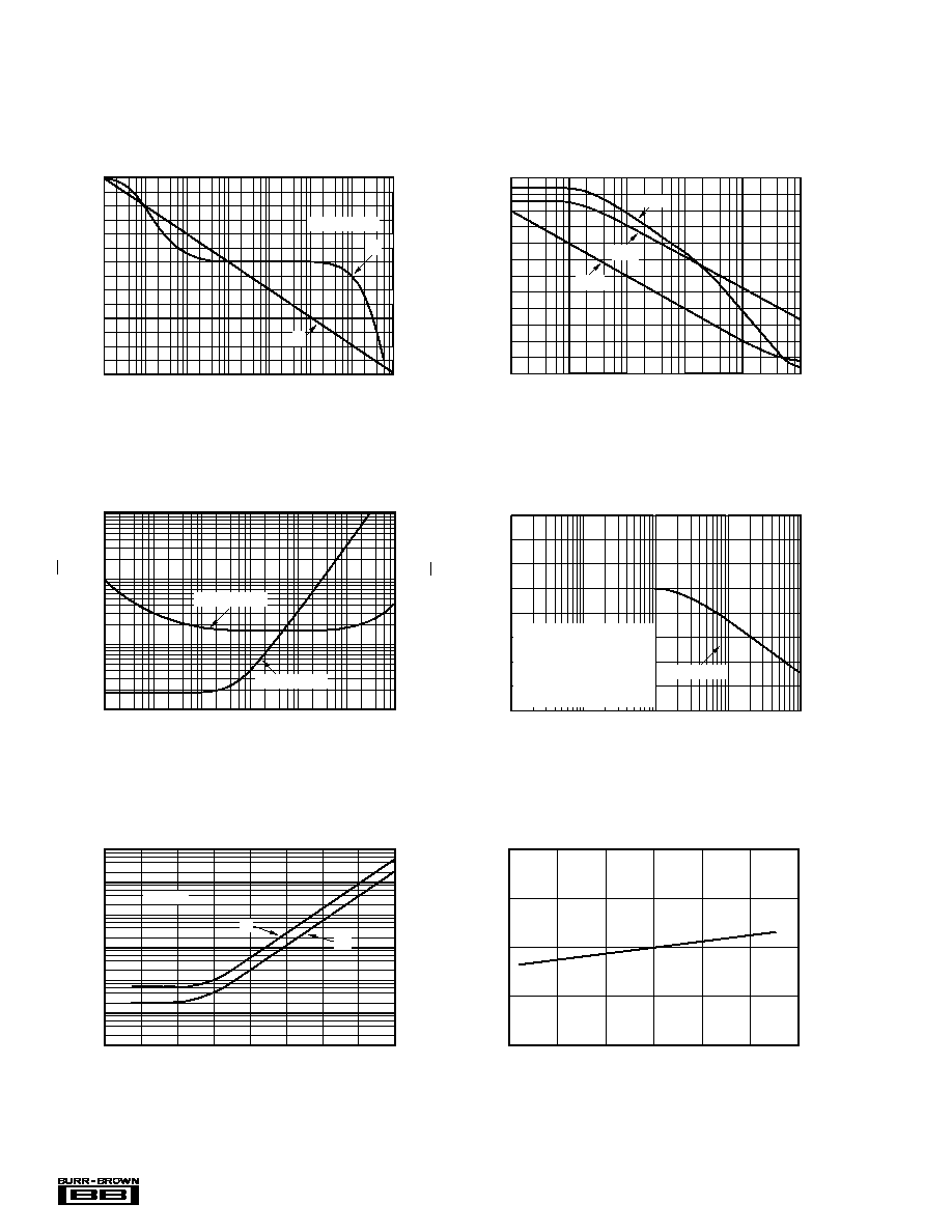
INPUT VOLTAGE AND CURRENT NOISE
SPECTRAL DENSITY vs FREQUENCY
1
1k
100
10
Voltage Noise (nV/
Hz)
Frequency (Hz)
10
100
1k
10k
100k
1M
1
1k
100
10
Current Noise (fA/
Hz)
1
Voltage Noise
Current Noise
INPUT BIAS CURRENT
vs INPUT COMMON-MODE VOLTAGE
Common-Mode Voltage (V)
Input Bias Current (pA)
10
5
0
≠15
≠10
≠5
0
5
10
15
INPUT BIAS AND INPUT OFFSET CURRENT
vs TEMPERATURE
Ambient Temperature (∞C)
Input Bias and Input Offset Current (pA)
10k
1k
100
10
1
0.1
0.01
≠75
≠50
≠25
0
25
50
75
100
125
I
B
I
OS
V
CM
= 0V
CHANNEL SEPARATION vs FREQUENCY
Frequency (Hz)
Channel Separation (dB)
160
140
120
100
80
10
100
1k
10k
100k
Dual and quad devices.
G = 1, all channels.
Quad measured channel
A to D or B to C--other
combinations yield improved
rejection.
R
L
= 10k
OPEN-LOOP GAIN/PHASE vs FREQUENCY
1
120
100
80
60
40
20
0
≠20
Voltage Gain (dB)
0
≠45
≠90
≠135
≠180
Phase Shift (∞)
Frequency (Hz)
10
100
1k
10k
100k
1M
10M
G
C
L
= 100pF
POWER SUPPLY AND COMMON-MODE REJECTION
vs FREQUENCY
Frequency (Hz)
PSR, CMR (dB)
120
110
100
90
80
70
60
50
40
30
20
10
0
10
100
1k
10k
100k
1M
CMR
+PSR
≠PSR
5
OPA130, 2130, 4130
Æ
TYPICAL PERFORMANCE CURVES
(CONT)
At T
A
= +25
∞
C, V
S
=
±
15V, and R
L
= 10k
, unless otherwise noted.
MAXIMUM OUTPUT VOLTAGE
vs FREQUENCY
1M
Frequency (Hz)
10k
100k
30
25
20
15
10
5
0
Output Voltage (Vp-p)
V
S
= ±2.25V
V
S
= ±5V
Maximum output voltage
without slew-rate induced
distortion
V
S
= ±15V
OFFSET VOLTAGE
PRODUCTION DISTRIBUTION
Percent of Amplifiers (%)
Offset Voltage (µV)
≠700
≠600
≠500
≠400
≠300
≠200
≠100
0
100
200
300
400
500
600
700
15
10
5
0
OFFSET VOLTAGE DRIFT
PRODUCTION DISTRIBUTION
Percent of Amplifiers (%)
Offset Voltage Drift (µV/∞C)
20
18
16
14
12
10
8
6
4
2
0
0.00
0.50
1.00
1.50
2.00
2.50
3.00
3.50
4.00
4.50
5.00
5.50
6.00
6.50
7.00
7.50
8.00
A
OL
, CMR, PSR vs TEMPERATURE
Ambient Temperature (∞C)
A
OL
, CMR, PSR (dB)
140
130
120
110
100
≠75
≠50
≠25
0
25
50
75
100
125
CMR
Open-Loop
Gain
PSR
QUIESCENT CURRENT AND SHORT-CIRCUIT CURRENT
vs TEMPERATURE
Temperature (∞C)
Quiescent Current Per Amp (mA)
0.65
0.60
0.55
0.50
0.45
0.40
0.35
Short-Circuit Current (mA)
40
35
30
25
20
15
10
≠75
≠50
≠25
0
25
50
75
100
125
I
SC
+
I
Q
I
SC
≠
TOTAL HARMONIC DISTORTION + NOISE
vs FREQUENCY
Frequency (Hz)
THD + Noise (%)
0.1
0.01
0.001
0.0001
100
1k
10k
100k
G = +1
G = +10
R
L
= 10k
R
L
= 2k
6
Æ
OPA130, 2130, 4130
TYPICAL PERFORMANCE CURVES
(CONT)
At T
A
= +25
∞
C, V
S
=
±
15V, and R
L
= 10k
, unless otherwise noted.
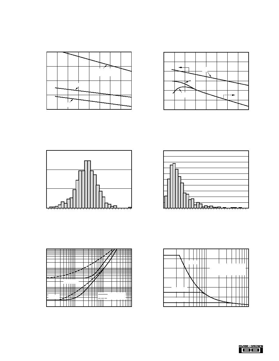
LARGE-SIGNAL STEP RESPONSE
G = 1, C
L
= 100pF
5V/div
5µs/div
SMALL-SIGNAL STEP RESPONSE
G =1, C
L
= 100pF
500ns/div
50mV/div
OUTPUT VOLTAGE SWING vs OUTPUT CURRENT
15
14
13
12
11
10
≠10
≠11
≠12
≠13
≠14
≠15
0
±5
±10
±15
±20
Output Current (mA)
Output Voltage Swing (V)
+125∞C
+25∞C
≠55∞C
+85∞C
+125∞C
+25∞C
≠55∞C
SMALL-SIGNAL STEP RESPONSE
G = 1, C
L
= 1000pF
50mV/div
5µs/div
SMALL-SIGNAL OVERSHOOT
vs LOAD CAPACITANCE
80
70
60
50
40
30
20
10
0
10pF
100pF
1nF
10nF
100nF
Load Capacitance (F)
Overshoot (%)
G = +1
G = ≠1
G = ±5
SETTLING TIME vs GAIN
Gain (V/V)
Settling Time (µs)
100
10
1
±1
±10
±100
0.1%
0.01%
7
OPA130, 2130, 4130
Æ
APPLICATIONS INFORMATION
OPA130 series op amps are unity-gain stable and suitable
for a wide range of general-purpose applications. Power
supply pins should be bypassed with 10nF ceramic capaci-
tors or larger.
OPA130 op amps are free from unexpected output phase-
reversal common with FET op amps. Many FET-input op
amps exhibit phase-reversal of the output when the input
common-mode voltage range is exceeded. This can occur in
voltage-follower circuits, causing serious problems in
control loop applications. OPA130 series op amps are free
from this undesirable behavior. All circuitry is completely
independent in dual and quad versions, assuring normal
behavior when one amplifier in a package is overdriven or
short-circuited.
OPERATING VOLTAGE
OPA130 series op amps operate with power supplies from
±
2.25V to
±
18V with excellent performance. Although
specifications are production tested with
±
15V supplies,
most behavior remains unchanged throughout the full
operating voltage range. Parameters which vary signifi-
cantly with operating voltage are shown in the typical
performance curves.
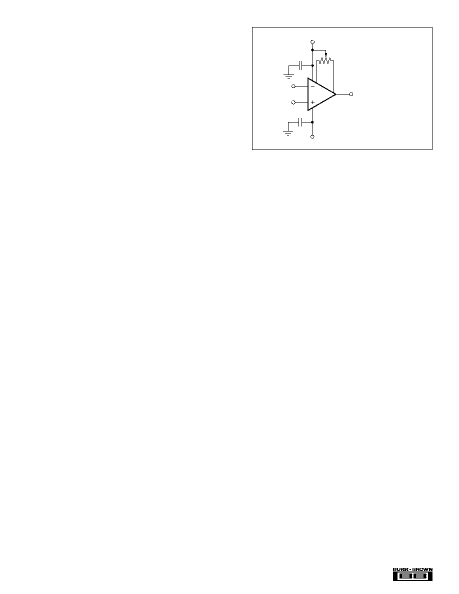
OFFSET VOLTAGE TRIM
Offset voltage of OPA130 series amplifiers is laser trimmed
and usually requires no user adjustment. The OPA130
(single op amp version) provides offset voltage trim con-
nections on pins 1 and 5. Offset voltage can be adjusted by
connecting a potentiometer as shown in Figure 1. This
adjustment should be used only to null the offset of the op
amp, not to adjust system offset or offset produced by the
signal source. Nulling offset that is not produced by the
amplifier will change the offset voltage drift behavior of
the op amp.
V+
V≠
100k
OPA130 single op amp only.
Use offset adjust pins only to null
offset voltage of op amp--see text.
Trim Range: ±5mV typ
OPA130
6
7
5
4
3
2
1
10nF
10nF
FIGURE 1. OPA130 Offset Voltage Trim Circuit.
INPUT BIAS CURRENT
The input bias current is approximately 5pA at room tem-
perature and increases with temperature as shown in the
typical performance curve "Input Bias Current vs Tempera-
ture."
Input stage cascode circuitry assures that the input bias
current remains virtually unchanged throughout the full
input common-mode range of the OPA130. See the typical
performance curve "Input Bias Current vs Common-Mode
Voltage."

IMPORTANT NOTICE
Texas Instruments and its subsidiaries (TI) reserve the right to make changes to their products or to discontinue
any product or service without notice, and advise customers to obtain the latest version of relevant information
to verify, before placing orders, that information being relied on is current and complete. All products are sold
subject to the terms and conditions of sale supplied at the time of order acknowledgment, including those
pertaining to warranty, patent infringement, and limitation of liability.
TI warrants performance of its semiconductor products to the specifications applicable at the time of sale in
accordance with TI's standard warranty. Testing and other quality control techniques are utilized to the extent
TI deems necessary to support this warranty. Specific testing of all parameters of each device is not necessarily
performed, except those mandated by government requirements.
Customers are responsible for their applications using TI components.
In order to minimize risks associated with the customer's applications, adequate design and operating
safeguards must be provided by the customer to minimize inherent or procedural hazards.
TI assumes no liability for applications assistance or customer product design. TI does not warrant or represent
that any license, either express or implied, is granted under any patent right, copyright, mask work right, or other
intellectual property right of TI covering or relating to any combination, machine, or process in which such
semiconductor products or services might be or are used. TI's publication of information regarding any third
party's products or services does not constitute TI's approval, warranty or endorsement thereof.
Copyright
©
2000, Texas Instruments Incorporated